Thank you for visiting nature.com. You are using a browser version with limited support for CSS. To obtain
the best experience, we recommend you use a more up to date browser (or turn off compatibility mode in
Internet Explorer). In the meantime, to ensure continued support, we are displaying the site without styles
and JavaScript.
The ability to genetically modify haematopoietic stem cells would allow the durable treatment of a diverse range of genetic disorders but gene delivery to the bone marrow has not been achieved. Here lipid nanoparticles that target and deliver mRNA to 14 unique cells within the bone marrow are presented.
Atomic force microscopy (AFM) is coupled with time-domain two-dimensional infrared (2DIR) spectroscopy to develop AFM-2DIR nanospectroscopy, which combines the spatial precision of AFM with the rich spectroscopic information provided by 2DIR spectroscopy. Application of this method reveals the anharmonicity of a carbonyl vibrational mode and the possible energy transfer pathways of hyperbolic phonon polaritons in isotope-rich hexagonal boron nitride.
Advances in nanoscale engineering bring us closer to unlocking the full potential of perovskite light-emitting diodes for future lighting and display applications.
A single monolayer semiconductor integrated into a plasmonic tunnel junction exhibits electroluminescence with photon energies that exceed the excitation electron potential. This phenomenon is shown to be indirectly triggered by inelastically tunnelling electrons.
FRETfluors—nanostructures with Cy3 and Cy5 dyes and a DNA scaffold—are used to generate distinct spectroscopic signals from different configurations and mixtures of mRNA, dsDNA and proteins in an anti-Brownian electrokinetic trap for single-molecule multiplexed sensing.
Integrating atomic force microscopy with time-domain two-dimensional infrared spectroscopy provides insights into molecular structures, mode coupling and energy transfers with high spatial resolution.
Superionic fluoride dielectrics with a low ion migration barrier are capable of excellent capacitive coupling and are highly compatible with scalable device manufacturing processes for integrated electronics.
This analysis leverages a large-scale literature review, text mining, statistics and machine learning to identify trends, shortcomings and future opportunities in developing and deploying inorganic nanoparticles for cancer diagnosis and therapy.
Antibacterial action, along with restoration of redox and immune homeostasis, is achieved using a lipid–nanozyme hybrid for the healing of diabetic foot ulcers.
Therapies for treating bacterial infection and increasing wound healing are needed. Here the authors report a liposozyme that combines reactive oxygen species generation and scavenging for antibacterial action and modulation of redox and immune homeostasis, increasing wound healing.
Increased nutrient uptake of cancer cells offers a possible therapeutic target. Here, the authors designed a nanoparticle to deliver phenylboronic-acid-modified cholesterol which reacts in cancer cells to trigger Gaucher disease-like metabolic damage to tumour cells, demonstrating potential application.
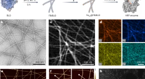
Oral antidotes for consumption-related acute alcohol intoxication are needed. Here, the study presents amyloid fibrils of β-lactoglobulin, a milk-derived protein decorated by single-site iron, as a catalytic platform for alcohol detoxification in vivo and prophylactic protection against alcohol damage.
Silver nanowires self-assembled on microscale elastomer pores, through in situ phase separation, yield highly elastic porous nanocomposite conductors with ultralow percolation threshold and high stretchability. This material is highly conductive, strain-insensitive and fatigue-tolerant, and holds promise for strain-resilient, wireless, battery-free bioelectronics.
A flow-through redox-neutral electrochemical reactor–electrodialysis system has been developed to recover water, alkali and acids from hypersaline wastewaters. This accelerates a shift in ‘zero-discharge’ technology from energy-intensive steam-driven to energy-efficient electrically driven processes.
By manipulating the glass transition of the electrolyte, nanometre-resolution electrochemical ion implantation doping can be achieved in various polymeric semiconductors.
The ability to vaccinate against multiple related pathogens is a significant advantage. Here, the authors report on quartets of linked receptor-binding domains attached to designed nanocages using SpyTag/SpyCatcher links, demonstrating effective vaccination against similar viruses as well as the variant of concern.
The emission wavelengths of semiconductor lasers based on group-IV materials can be efficiently reconfigured by using strained nanomechanical resonators.