Thank you for visiting nature.com. You are using a browser version with limited support for CSS. To obtain
the best experience, we recommend you use a more up to date browser (or turn off compatibility mode in
Internet Explorer). In the meantime, to ensure continued support, we are displaying the site without styles
and JavaScript.
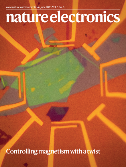
The magnetism in twisted double bilayers of antiferromagnetic chromium triiodide can be controlled via twist angle, temperature and electrical gating. The optical microscopy image on the cover shows a back-gated chromium triiodide device in which flakes of bilayer chromium triiodide are encapsulated within flakes of hexagonal boron nitride and contacted via a few-layer graphene flake; this stack is placed on prepatterned gold electrodes on a silicon wafer.
The capabilities of touchless user interfaces that recognize hand gestures are improving, but their place in the future of everyday electronics remains uncertain.
Stacking a bilayer of chromium triiodide, a layered antiferromagnet, onto another with a twist angle gives rise to a moiré magnet with rich magnetic phases, including ferromagnetic and antiferromagnetic orders. The magnetic orders can be controlled through the twist angle, temperature and electrical gating, with the system also showing voltage-assisted magnetic switching.
A technique based on a scanning tunnelling microscope can provide simultaneous control, visualization and spectroscopic characterization of quantum states with atomic resolution.
A magnetic random-access memory device that has an antiferromagnetic material as its storage element can be electrically read using ferromagnetic tunnelling.
A scanning tunnelling microscope, operating on an insulating substrate, can be used to perform spatially resolved wavefunction spectroscopy and local gate control of a quantum dot device consisting of phosphorus atoms in silicon.
Strontium titanate two-dimensional electron gas channels that have a thin hafnium oxide barrier layer between the channel and an ionic liquid gate can have ballistic constrictions and clean normal-state conductance quantization.
Antiferromagnetism of the IrMn layer in Pt/IrMn/CoFeB/MgO/CoFeB three-terminal magnetic tunnel junctions can be electrically detected using tunnelling magnetoresistance and controlled by a spin–orbit torque generated by a 0.8 ns current pulse applied across the heavy-metal platinum layer.
The magnetic state of twisted double bilayers of antiferromagnetic chromium triiodide can be controlled by electrical gating, twist angle and temperature.
Arrays of thin-film transistors can be fabricated on the 5-inch wafer scale using solution-based processing of molybdenum disulfide and sodium-embedded alumina inks for the semiconductor and gate dielectric, respectively, yielding devices with room-temperature mobilities of up to 80 cm2 V−1 s−1.