
Production of 2D Materials
- Submission status
- Open
- Submission deadline
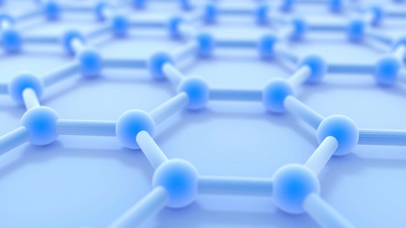
Numerous potential applications in electronics, photonics, energy storage, catalysis, sensing, and other fields are made possible by the special qualities of 2D materials. The isolation of graphene in 2004 provided a major impetus for the investigation of 2D materials. After graphene was discovered, scientists started looking at additional 2D materials, such as tungsten diselenide (WSe2) and molybdenum disulfide (MoS2). These are examples of transition metal dichalcogenides (TMDs). Several synthesis methods have been created to create 2D materials with various characteristics and uses. These methods include liquid-phase exfoliation, chemical vapor deposition (CVD), mechanical exfoliation (the Scotch tape method used for graphene), and different bottom-up approaches.
At first, 2D material production was restricted to small-scale lab synthesis. Nonetheless, in order to satisfy industrial demands, researchers have been working on scalable production techniques. This entails creating efficient production techniques, enhancing material quality and yield, and streamlining synthesis procedures. Research efforts have been focused on characterizing the characteristics and behavior of 2D materials at the nanoscale, in addition to their synthesis and applications. To comprehend their electrical, optical, mechanical, and chemical properties, methods including spectroscopy, transmission electron microscopy, and scanning probe microscopy are employed.
This Collection welcome the following topics, including but not limited to:
- Synthesis Techniques
- Scaling Up Production
- Functionalization and Modification
- Characterization Methods
- Properties and Performance
- Applications
Editors
-
Deji Akinwande, PhD
University of Texas at Austin, USA
-
Hyeon Suk Shin, PhD
Sungkyunkwan University(SKKU), Republic of Korea


