Thank you for visiting nature.com. You are using a browser version with limited support for CSS. To obtain
the best experience, we recommend you use a more up to date browser (or turn off compatibility mode in
Internet Explorer). In the meantime, to ensure continued support, we are displaying the site without styles
and JavaScript.
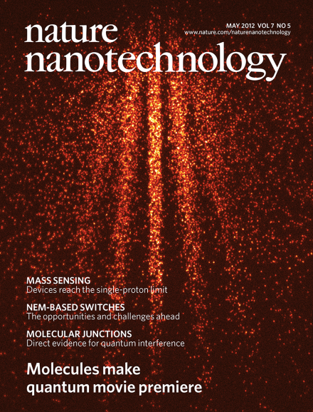
The observation of interference patterns in double-slit experiments with massive particles is generally regarded as the ultimate demonstration of the quantum nature of these particles. Moreover, unlike what happens in classical physics, it is possible to watch the build up of the pattern as the particles arrive at the detector one by one. Now researchers from Vienna, Tel Aviv and Basel have used a combination of nanofabrication and nanoimaging to record these patterns building up in real time for molecules with a mass of 1,298â AMU, which is a new record for such experiments, and 514â AMU (see cover; image measures 320â μm across). Last year many of the same researchers observed quantum interference of even heavier molecules (6,910â AMU) but did not record the build up of the interference pattern in thoseâ experiments.
A direct current flowing through a carbon nanotube on a substrate heats the substrate but not the nanotube, and it may be possible to exploit this phenomenon in the thermal management of nanoelectronic devices.
An atomic force microscope with a gold-coated tip can be used to directly observe quantum interference in molecular monolayers adsorbed on gold substrates.
Nanoelectromechanical (NEM) switches have the potential to complement or selectively replace conventional semiconductor technology. This Review discusses the challenges involved in the large-scale manufacture of a representative set of NEMS-based devices.
A nanofabricated diffraction grating and single-molecule imaging are used to record the build up of the quantum interference patterns for molecules with masses as high as 1,298 AMU.
A carbon nanotube resonator is used to form the basis of an ultrasensitive mass sensor that can also be employed to study basic phenomena in surface science.
The results of simultaneous measurements of the structure and optical properties of more than 200 single-walled carbon nanotubes are reported and included in an atlas that allows the chiral index of any single-walled nanotube to be determined from a measurement of its optical resonances, and vice versa.
The resonant frequency and magnitude of graphene plasmons in graphene/insulator stacks depend on the layer number, which allows tunable filters and polarizers to be built.
Films of densely packed core–shell quantum dots demonstrate full-colour amplified spontaneous emission with single-exciton gain, and are used to build vertical-cavity surface-emitting lasers operating at very low optical pumping thresholds.