Thank you for visiting nature.com. You are using a browser version with limited support for CSS. To obtain
the best experience, we recommend you use a more up to date browser (or turn off compatibility mode in
Internet Explorer). In the meantime, to ensure continued support, we are displaying the site without styles
and JavaScript.
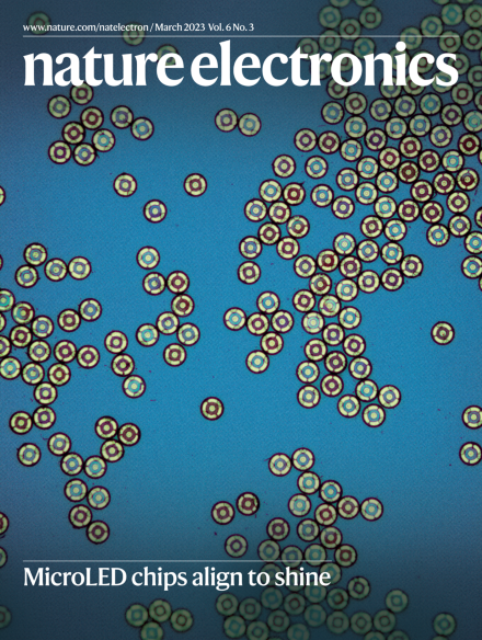
Micro-light-emitting-diode (microLED) chips can be accurately aligned on a substrate — and used to create active-matrix displays — by engineering the top and bottom faces of the chips so that they have a different van der Waals interaction with the substrate. The optical microscopy image on the cover shows the microLED chips on a silicon substrate, with the faces of the chips all aligned in the same direction.
Micro-light-emitting diodes — microLEDs — could be used to create the next generation of displays, for use in smartwatches and augmented reality devices, if various fabrication issues can be addressed.
By selectively engineering the surface roughness of micro-light-emitting-diode chips, and thus the strength of the van der Waals forces that bond them to a substrate, large-area displays can be created via a fluidic-assisted transfer method.
This Review examines the development of cryogenic memory technologies—including non-superconducting memories, superconducting memories and hybrid memories—and their potential application in superconducting single-flux quantum circuits and quantum computers.
Magnetic hysteresis in multiferroic heterostructures formed from the two-dimensional magnetic insulator chromium germanium telluride and a thin ferroelectric polymer can be electrically controlled with voltages of around 5 V.
An organogel that is based on poly(vinyl alcohol)–sodium borate and contains a percolating conductive network of silver particles and liquid metal microdroplets exhibits spontaneous mechanical and electrical self-healing, as well as an electrical conductivity of 7 × 10⁴ S m−1.
By engineering the upper and lower surfaces of micro-light-emitting-diode chips to have different van der Waals forces, hundreds and thousands of chips can be accurately aligned on substrates and used to create active-matrix displays.
Magnetic meta-atoms made from lanthanum-doped barium hexaferrite can be used to create self-biased non-reciprocal metasurfaces capable of unidirectional transmission, non-reciprocal beam steering, non-reciprocal beam focusing and non-reciprocal holography.
Low-loss superconducting aluminium cables and on-chip impedance transformers can be used to link qubit modules and create superconducting quantum computing networks with high-fidelity intermodule state transfer.
Wireless ingestible microdevices can be tracked through the gastrointestinal tract of large animals in real time and with millimetre-scale spatial resolution by generating three-dimensional magnetic field gradients in the gastrointestinal field-of-view using high-efficiency planar electromagnetic coils, which encode each spatial point with a distinct magnetic field magnitude.
Micro-light-emitting-diode display applications are growing quickly as technology companies begin to use them in a range of products. Key to the development of these applications was the miniaturization of gallium nitride light-emitting diodes. Hongxing Jiang and Jingyu Lin recount how this was achieved.