Thank you for visiting nature.com. You are using a browser version with limited support for CSS. To obtain
the best experience, we recommend you use a more up to date browser (or turn off compatibility mode in
Internet Explorer). In the meantime, to ensure continued support, we are displaying the site without styles
and JavaScript.
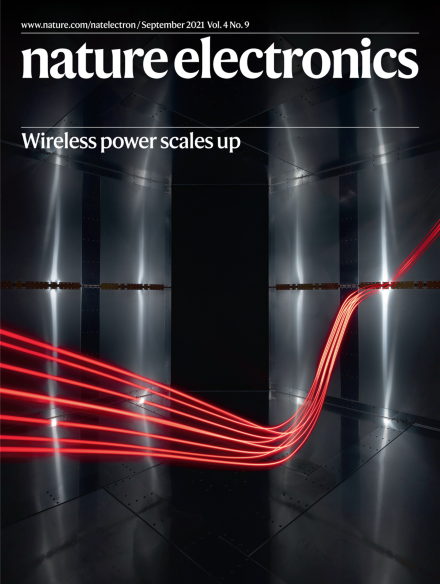
Multidirectional currents on conductive surfaces built into the walls of a room can generate widely distributed magnetic field patterns that wirelessly power electronic devices located anywhere in the room. The long-exposure photograph on the cover shows the path a wirelessly powered red light-emitting diode (LED) took as it was carried through a test room for the wireless power transfer technique.
This Perspective explores the potential of an approach to neuromorphic electronics in which the functional synaptic connectivity map of a mammalian neuronal network is copied using a silicon neuro-electronic interface and then pasted onto a high-density three-dimensional network of solid-state memories.
A light-detection electrochemical cell that is based on vertically aligned p–n heterojunction nanowires in an electrolyte environment can exhibit a photoresponse in which the polarity is reversed depending on the wavelength of light.
Narrow, long graphene nanoribbons with atomically smooth and defect-free edges can be produced by squashing carbon nanotubes, and can be used to fabricate a sub-3-nm-wide channel field-effect transistor with a mobility of 2,443 cm2 V−1 s−1.
Carriers in a molybdenum disulfide transistor can be modulated without decreasing mobility by remote doping and charge transfer through a van der Waals heterostructure, which avoids dopant-induced impurity scattering in the channel.
Two-dimensional arrays of quantum dot light-emitting diodes can be folded into three-dimensional architectures—including a passive matrix array that can display letters and numbers—by using laser patterning and metal etch-stop layers to create folding lines.
X-ray flat-panel detector arrays with high spatial resolution and sensitivity can be created using a two-step manufacturing process that separates the fabrication of microcrystalline methylammonium lead triiodide absorber wafers from their integration on pixelated backplanes.
Small electronic devices can be wirelessly powered from anywhere in a room using multidirectional surface currents that generate widely distributed three-dimensional magnetic field patterns.