Abstract
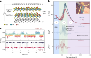
Fluctuations are ubiquitous in magnetic materials and can cause random telegraph noise. Such noise is of potential use in systems such as spiking neuron devices, random number generators and probability bits. Here we report electrically tunable magnetic fluctuations and random telegraph noise in multilayered vanadium-doped tungsten diselenide (WSe2) using vertical tunnelling heterostructure devices composed of graphene/vanadium-doped WSe2/graphene and magnetoresistance measurements. We identify bistable magnetic states through discrete Gaussian peaks in the random telegraph noise histogram and the 1/f2 features of the noise power spectrum. Three categories of fluctuation are detected: small resistance fluctuations at high temperatures due to intralayer coupling between the magnetic domains; large resistance changes over a wide range of temperatures; and persistent large resistance changes at low temperatures due to magnetic interlayer coupling. We also show that the bistable state and cut-off frequency of the random telegraph noise can be modulated with an electric bias.
This is a preview of subscription content, access via your institution
Access options
Access Nature and 54 other Nature Portfolio journals
Get Nature+, our best-value online-access subscription
$29.99 / 30 days
cancel any time
Subscribe to this journal
Receive 12 digital issues and online access to articles
$119.00 per year
only $9.92 per issue
Buy this article
- Purchase on Springer Link
- Instant access to full article PDF
Prices may be subject to local taxes which are calculated during checkout


Data availability
Source data are provided with this paper. All other data that support the plots within this paper and other findings of this study are available from the corresponding authors upon reasonable request.
References
Jevtić, M. M. Noise as a diagnostic and prediction tool in reliability physics. Microelectron. Reliab. 35, 455–477 (1995).
Grasser, T. Noise in Nanoscale Semiconductor Devices (Springer, 2020).
Grollier, J. et al. Neuromorphic spintronics. Nat. Electron. 3, 360–370 (2020).
Marković, D., Mizrahi, A., Querlioz, D. & Grollier, J. Physics for neuromorphic computing. Nat. Rev. Phys. 2, 499–510 (2020).
Camsari, K. Y., Faria, R., Sutton, B. M. & Datta, S. Stochastic p-bits for invertible logic. Phys. Rev. 7, 031014 (2017).
Camsari, K. Y., Sutton, B. M. & Datta, S. p-bits for probabilistic spin logic. Appl. Phys. Rev. 6, 011305 (2019).
Borders, W. A. et al. Integer factorization using stochastic magnetic tunnel junctions. Nature 573, 390–393 (2019).
Hayakawa, K. et al. Nanosecond random telegraph noise in in-plane magnetic tunnel junctions. Phys. Rev. Lett. 126, 117202 (2021).
Safranski, C. et al. Demonstration of nanosecond operation in stochastic magnetic tunnel junctions. Nano Lett. 21, 2040–2045 (2021).
Ghosh, S., Kargar, F., Mohammadzadeh, A., Rumyantsev, S. & Balandin, A. A. Low‐frequency electronic noise in quasi‐2D van der Waals antiferromagnetic semiconductor FePS3—signatures of phase transitions. Adv. Electron. Mater. 7, 2100408 (2021).
Kundu, H. K. et al. Quantum phase transition in few-layer NbSe2 probed through quantized conductance fluctuations. Phys. Rev. Lett. 119, 226802 (2017).
Valle, J. D. et al. Generation of tunable stochastic sequences using the insulator–metal transition. Nano Lett. 22, 1251–1256 (2022).
Weissman, M. B. & Israeloff, N. E. Electrical noise measurements on magnetic films (invited). J. Appl. Phys. 67, 4884–4888 (1990).
Raquet, B., Anane, A., Wirth, S., Xiong, P. & Von Molnár, S. Noise probe of the dynamic phase separation in La2/3Ca1/3MnO3. Phys. Rev. Lett. 84, 4485–4488 (2000).
Collins, M. F. Magnetic Critical Scattering (Oxford Univ. Press, 1989).
Mermin, N. D. & Wagner, H. Absence of ferromagnetism or antiferromagnetism in one- or two-dimensional isotropic Heisenberg models. Phys. Rev. Lett. 17, 1133–1136 (1966).
Jin, C. et al. Imaging and control of critical fluctuations in two-dimensional magnets. Nat. Mater. 19, 1290–1294 (2020).
Nair, G. K. R. et al. Phase-pure two-dimensional FexGeTe2 magnets with near-room-temperature TC. Nano Res. 15, 457–464 (2022).
Yun, S. J. et al. Ferromagnetic order at room temperature in monolayer WSe2 semiconductor via vanadium dopant. Adv. Sci. 7, 1903076 (2020).
Song, B. et al. Evidence of itinerant holes for long-range magnetic order in tungsten diselenide semiconductor with vanadium dopants. Phys. Rev. B 103, 094432 (2020).
Jiang, J. et al. Probing giant Zeeman shift in vanadium-doped WSe2 via resonant magnetotunneling transport. Phys. Rev. B 103, 014441 (2021).
Merithew, R. D. et al. Mesoscopic thermodynamics of an inhomogeneous colossal-magnetoresistive phase. Phys. Rev. Lett. 84, 3442–3445 (2000).
Zhu, M., Li, X., Xiang, G. & Samarth, N. Random telegraph noise from magnetic nanoclusters in the ferromagnetic semiconductor (Ga,Mn)As. Phys. Rev. B 76, 201201 (2007).
Klein, D. R. et al. Probing magnetism in 2D van der Waals crystalline insulators via electron tunneling. Science 360, 1218–1222 (2018).
Song, T. et al. Giant tunneling magnetoresistance in spin-filter van der Waals heterostructures. Science 360, 1214–1218 (2018).
Huang, B. et al. Electrical control of 2D magnetism in bilayer CrI3. Nat. Nanotechnol. 13, 544–548 (2018).
Jiang, S., Shan, J. & Mak, K. F. Electric-field switching of two-dimensional van der Waals magnets. Nat. Mater. 17, 406–410 (2018).
Baibich, M. N. et al. Giant magnetoresistance of (001)Fe/(001)Cr magnetic superlattices. Phys. Rev. Lett. 61, 2472–2475 (1988).
Yuasa, S., Nagahama, T., Fukushima, A., Suzuki, Y. & Ando, K. Giant room-temperature magnetoresistance in single-crystal Fe/MgO/Fe magnetic tunnel junctions. Nat. Mater. 3, 868–871 (2004).
Parkin, S. S. P. et al. Giant tunnelling magnetoresistance at room temperature with MgO (100) tunnel barriers. Nat. Mater. 3, 862–867 (2004).
Telford, E. J. et al. Coupling between magnetic order and charge transport in a two-dimensional magnetic semiconductor. Nat. Mater. 21, 754–760 (2022).
Ohta, T. et al. Butterfly-shaped magnetoresistance in van der Waals ferromagnet Fe5GeTe2. AIP Adv. 11, 025014 (2021).
Zhuo, W. et al. Manipulating ferromagnetism in few‐layered Cr2Ge2Te6. Adv. Mater. 33, 2008586 (2021).
Cao, W., Wei-Yuan Tu, M., Xiao, J. & Yao, W. Giant spin transfer torque in atomically thin magnetic bilayers. Chinese Phys. Lett. 37, 107201 (2020).
Coey, J. M. D. Magnetism and Magnetic Materials (Cambridge Univ. Press, 2001).
Song, B. et al. Evidence of itinerant holes for long-range magnetic order in the tungsten diselenide semiconductor with vanadium dopants. Phys. Rev. B 103, 094432 (2021).
Li, Q. et al. Correlation between particle size/domain structure and magnetic properties of highly crystalline Fe3O4 nanoparticles. Sci. Rep. 7, 9894 (2017).
Acknowledgements
This work was supported by the Institute for Basic Science (IBS-R011-D1) and Advanced Facility Center for Quantum Technology. P.K. acknowledges partial support from ARO (W911NF-18-1-0366). M.-K.J. was supported by an NRF grant funded by the Korean government (MSIT) (NRF-2022R1A2C4001245) and by Sookmyung Women’s University Research Grants (1-2203-2001).
Author information
Authors and Affiliations
Contributions
L.-A.T.N., J.J. and D.L.D. initiated this work. L.-A.T.N. fabricated and characterized the devices. T.D.N. synthesized the V-WSe2 single crystals. M.-K.J. performed the noise analysis. D.L.D. and Y.H.L. guided the work. L.-A.T.N., P.K., M.-K.J., D.L.D. and Y.H.L. analysed the data. All authors discussed and wrote the manuscript.
Corresponding authors
Ethics declarations
Competing interests
The authors declare no competing interests.
Peer review
Peer review information
Nature Electronics thanks the anonymous reviewers for their contribution to the peer review of this work.
Additional information
Publisher’s note Springer Nature remains neutral with regard to jurisdictional claims in published maps and institutional affiliations.
Extended data
Extended Data Fig. 1 In-plane and out-of-plane MR hysteresis of 0.3% V-doped WSe2 for the same bias of 0.85 mV at different temperatures.
Out-of-plane MR hysteresis curve (> 3 T) is much larger than in-plane MR hysteresis curve (~1.5 T) at 2 K. MR hysteresis persists at higher temperatures in out-of-plane direction, whereas it is obscured in in-plane direction. This indicates the easy axis in-plane magnetic order.
Extended Data Fig. 2 In-plane and out-of-plane MR hysteresis of 0.1%, 0.3%, and 0.5% V-doped WSe2 at 2 K.
MR hysteresis is distinctly manifested at 0.3% and 0.5% V, confirming the stable ferromagnetic states. MR hysteresis is obscured at 0.1% V, indicating unstable magnetic states. All samples are the same thickness of ~ 2 nm. The biases of 0.8 V, 0.85 mV, and 0.5 mV are applied for corresponding 0.1%, 0.3%, and 0.5% V-doped WSe2.
Extended Data Fig. 3 RTN signals after FC with out-of-plane and in-plane 1 T magnetic fields.
The data were measured at 30 K with -0.9 V and +0.9 V in device 5.
Extended Data Fig. 4 Complete data on temperature-dependent RTN signals across the Gr/V-WSe2/Gr after FC at -0.9 V in device 1.
Time evolution of RTNs in the high (160–300 K), intermediate (70–140 K), and low temperature regions (2–60 K).
Extended Data Fig. 5 Control of RTNs with bias changes at 2 K after ZFC and FC at 1 T for a given thinner sample of 2 nm-thick 0.1% V-doped WSe2.
Note that the resistance was significantly reduced in an order of kΩ, compared to Fig. 5c with a sample thickness of 5 nm (device 7). The number of jumps increases with increasing biases, similar to the data in Fig. 5c in of device 2, confirming the bias-controlled number of jumps in both ZFC and FC.
Extended Data Fig. 6 Control of RTN signals after ZFC by positive biases in device 2.
The effect was similar to that seen with negative biases (Fig. 5c).
Extended Data Fig. 7 Control of RTN signals by biases at 120 K after FC of 1 T in device 1.
The frequency increased from ~0.1 Hz at -0.85 V to ~1.7 Hz at -0.95 V. The control of device speed becomes slower when applying too high magnetic field during FC that induces too stable magnetic states.
Extended Data Fig. 8
Switching capability of bistable state of parallel and antiparallel states by using two polarities of biases at + 0.9 V and -0.9 V after FC at 1 T and 40 K in device 1.
Extended Data Fig. 9 Representative bitmap image constructed by the obtained RTN data stream in bottom of Fig. 5c (4,096 points).
a, Measured RTNs at 2 K and −0.95 V after ZFC. b, Bitmap image realized by 4 k bits of the generated RTNs as a potential application for true random number generator (top) and corresponding digitized image (Bottom). c, Bitmap images by 40 k bits of the generated RTNs, where the RTN data stream of Extended Data Fig. 9b was stacked by 10 times.
Extended Data Table. 10
RTNs after ZFC at -0.7 V, 300 K with a size of 1×1 µm2 in device 6.
Supplementary information
Supplementary Information
Supplementary Figs. 1–14 and note.
Supplementary Data
Compressed file comprising source data for Supplementary Figs. 1–9, 11 and 13.
Source data
Source Data Fig. 1
Resistance changes with temperature and the identification of giant RTN in a vertical graphene/V-WSe2/graphene device.
Source Data Fig. 2
MR hysteresis in V-doped WSe2 at different V-doping concentrations.
Source Data Fig. 3
Control of RTN by magnetic fields.
Source Data Fig. 4
Temperature-dependent RTN across the vertical graphene/V-WSe2/graphene junction after FC.
Source Data Fig. 5
Control of RTNs across the vertical graphene/V-WSe2/graphene junction by biases after ZFC process.
Source Data Extended Data Fig. 1
In-plane and out-of-plane MR hysteresis of 0.3% V-doped WSe2 for the same bias of 0.85 mV at different temperatures.
Source Data Extended Data Fig. 2
In-plane and out-of-plane MR hysteresis of 0.1%, 0.3% and 0.5% V-doped WSe2 at 2 K.
Source Data Extended Data Fig. 3
RTN signals after FC with out-of-plane and in-plane 1 T magnetic fields.
Source Data Extended Data Fig. 4
Complete data on temperature-dependent RTN signals across the graphene/V-WSe2/graphene after FC at –0.9 V in device 1.
Source Data Extended Data Fig. 5
Control of RTNs with bias changes at 2 K after ZFC and FC at 1 T for a given thinner sample of 2-nm-thick 0.1% V-doped WSe2.
Source Data Extended Data Fig. 6
Control of RTN signals after ZFC by positive biases in device 2.
Source Data Extended Data Fig. 7
Control of RTN signals by biases at 120 K after FC of 1 T in device 1.
Source Data Extended Data Fig. 8
Switching capability of the bistable state of P and AP states by using two polarities of biases at +0.9 and –0.9 V after FC at 1 T and 40 K in device 1.
Source Data Extended Data Fig. 9
Representative bitmap image constructed by the obtained RTN data stream in bottom of Fig. 5c (4,096 points).
Source Data Extended Data Fig. 10
RTNs after ZFC at –0.7 V, 300 K with a size of 1 × 1 µm2 in device 6.
Rights and permissions
Springer Nature or its licensor (e.g. a society or other partner) holds exclusive rights to this article under a publishing agreement with the author(s) or other rightsholder(s); author self-archiving of the accepted manuscript version of this article is solely governed by the terms of such publishing agreement and applicable law.
About this article
Cite this article
Nguyen, LA.T., Jiang, J., Nguyen, T.D. et al. Electrically tunable magnetic fluctuations in multilayered vanadium-doped tungsten diselenide. Nat Electron 6, 582–589 (2023). https://doi.org/10.1038/s41928-023-01002-1
Received:
Accepted:
Published:
Issue Date:
DOI: https://doi.org/10.1038/s41928-023-01002-1


