Thank you for visiting nature.com. You are using a browser version with limited support for CSS. To obtain
the best experience, we recommend you use a more up to date browser (or turn off compatibility mode in
Internet Explorer). In the meantime, to ensure continued support, we are displaying the site without styles
and JavaScript.
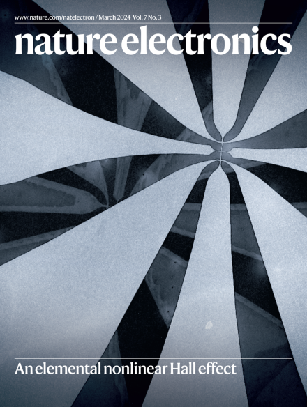
Thin films of the element bismuth — an environmentally friendly and scalable material — can exhibit a tunable room-temperature nonlinear Hall effect, which could be of use in the development of optoelectronic devices. The scanning electron microscopy image on the cover shows a bismuth Hall cross device, which is used to explore magnetotransport and the nonlinear Hall effect in the polycrystalline thin films.
Wearable sweat sensors could be used to monitor patients with heart failure, providing a route to personalized and automated patient management in hospitals and at home.
Polycrystalline films of the non-toxic element bismuth exhibit a room-temperature surface nonlinear Hall effect, which could make devices based on topological quantum effects more practical.
An approach to dynamically control the photoresponsivity of pixels in a computational sensor based on local image gradients enables the precise and robust detection of edge features of targets in dim light conditions from a single image capture.
This Review examines the development of electrical reservoir computing, considering the architectures, physical nodes, and input and output layers of the approach, as well as performance benchmarks and the competitiveness of different implementations.
Polycrystalline thin films of elemental bismuth exhibit a room-temperature nonlinear transverse voltage due to geometric effects of surface electrons that is tunable and can be extended to efficient high-harmonic generation at terahertz frequencies.
A two-dimensional perovskite, Sr2Nb3O10, can be integrated with a range of other two-dimensional materials and act as a photoactive high-κ dielectric in the resulting phototransistors.
The correlated optoelectronic characteristics of multi-terminal mixed-dimensional graphene–germanium heterostructure devices can be used for the accurate detection and robust tracking of dim targets.
Micropatterning of organic semiconductors by electron-beam exposure can be used to create vertical organic electrochemical transistor arrays and complementary logic circuits with densities of up to 7.2 million transistors per cm2.
Developments in universal chiplet interconnect express could be used to construct three-dimensional system-on-chip design architectures that offer power, performance and reliability characteristics approaching or exceeding those of current monolithic system-on-chip designs as the bump interconnect pitch approaches 1 µm.