Abstract
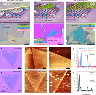
Beyond-silicon technology demands ultrahigh performance field-effect transistors. Transition metal dichalcogenides provide an ideal material platform, but the device performances such as the contact resistance, on/off ratio and mobility are often limited by the presence of interfacial residues caused by transfer procedures. Here, we show an ideal residue-free transfer approach using polypropylene carbonate with a negligible residue coverage of ~0.08% for monolayer MoS2 at the centimetre scale. By incorporating a bismuth semimetal contact with an atomically clean monolayer MoS2 field-effect transistor on hexagonal boron nitride substrate, we obtain an ultralow Ohmic contact resistance of ~78 Ω µm, approaching the quantum limit, and a record-high on/off ratio of ~1011 at 15 K. Such an ultra-clean fabrication approach could be the ideal platform for high-performance electrical devices using large-area semiconducting transition metal dichalcogenides.
This is a preview of subscription content, access via your institution
Access options
Access Nature and 54 other Nature Portfolio journals
Get Nature+, our best-value online-access subscription
$29.99 / 30 days
cancel any time
Subscribe to this journal
Receive 12 print issues and online access
$259.00 per year
only $21.58 per issue
Buy this article
- Purchase on Springer Link
- Instant access to full article PDF
Prices may be subject to local taxes which are calculated during checkout


Data availability
The data that support the findings of this study are available from the corresponding authors upon reasonable request.
References
Liu, C. et al. Two-dimensional materials for next-generation computing technologies. Nat. Nanotechnol. 15, 545–557 (2020).
Jung, S.-G., Kim, J.-K. & Yu, H.-Y. Analytical model of contact resistance in vertically stacked nanosheet FETs for sub-3-nm technology node. IEEE Trans. Electron Devices 69, 930–935 (2022).
Watson, A. J., Lu, W., Guimarães, M. H. D. & Stöhr, M. Transfer of large-scale two-dimensional semiconductors: challenges and developments. 2D Mater. 8, 032001 (2021).
Zhang, S. et al. Wafer-scale transferred multilayer MoS2 for high performance field effect transistors. Nanotechnology 30, 174002 (2019).
Lee, J. S. et al. Wafer-scale single-crystal hexagonal boron nitride film via self-collimated grain formation. Science 362, 817–821 (2018).
Li, T. et al. Epitaxial growth of wafer-scale molybdenum disulfide semiconductor single crystals on sapphire. Nat. Nanotechnol. 16, 1201–1207 (2021).
Leong, W. S. et al. Paraffin-enabled graphene transfer. Nat. Commun. 10, 867 (2019).
Zhang, T. et al. Clean transfer of 2D transition metal dichalcogenides using cellulose acetate for atomic resolution characterizations. ACS Appl. Nano Mater. 2, 5320–5328 (2019).
Wang, P. et al. High-fidelity transfer of chemical vapor deposition grown 2D transition metal dichalcogenides via substrate decoupling and polymer/small molecule composite. ACS Nano 14, 7370–7379 (2020).
Wang, Y. et al. Van der Waals contacts between three-dimensional metals and two-dimensional semiconductors. Nature 568, 70–74 (2019).
Cui, X. et al. Low-temperature Ohmic contact to monolayer MoS2 by van der Waals bonded Co/h-BN electrodes. Nano Lett. 17, 4781–4786 (2017).
Kim, C. et al. Fermi level pinning at electrical metal contacts of monolayer molybdenum dichalcogenides. ACS Nano 11, 1588–1596 (2017).
English, C. D., Shine, G., Dorgan, V. E., Saraswat, K. C. & Pop, E. Improved contacts to MoS2 transistors by ultra-high vacuum metal deposition. Nano Lett. 16, 3824–3830 (2016).
Das, S., Chen, H.-Y., Penumatcha, A. V. & Appenzeller, J. High performance multilayer MoS2 transistors with scandium contacts. Nano Lett. 13, 100–105 (2013).
English, C. D., Smithe, K. K. H. & Pop, E. Approaching ballistic transport in monolayer MoS2 transistors with self-aligned 10 nm top gates. In Proc. 2016 IEEE International Electron Devices Meeting 131–134 (IEEE, 2016).
McClellan, C. J., Yalon, E., Smithe, K. K. H., Suryavanshi, S. V. & Pop, E. High current density in monolayer MoS2 doped by AlOx. ACS Nano 15, 1587–1596 (2021).
Smithe, K. K. H., Suryavanshi, S. V., Muñoz Rojo, M., Tedjarati, A. D. & Pop, E. Low variability in synthetic monolayer MoS2 devices. ACS Nano 11, 8456–8463 (2017).
Guimarães, M. H. D. et al. Atomically thin Ohmic edge contacts between two-dimensional materials. ACS Nano 10, 6392–6399 (2016).
Smets, Q. et al. Ultra-scaled MOCVD MoS2 MOSFETs with 42 nm contact pitch and 250 µA/µm drain current. In 2019 IEEE International Electron Devices Meeting 23.2.1–23.2.4 (IEEE, 2019).
Shen, P.-C. et al. Ultralow contact resistance between semimetal and monolayer semiconductors. Nature 593, 211–217 (2021).
Kim, B.-K. et al. Origins of genuine Ohmic van der Waals contact between indium and MoS2. npj 2D Mater. Appl. 5, 9 (2021).
Kinoshita, K. et al. Dry release transfer of graphene and few-layer h-BN by utilizing thermoplasticity of polypropylene carbonate. npj 2D Mater. Appl. 3, 22 (2019).
Frisenda, R. et al. Recent progress in the assembly of nanodevices and van der Waals heterostructures by deterministic placement of 2D materials. Chem. Soc. Rev. 47, 53–68 (2018).
Schranghamer, T. F., Sharma, M., Singh, R. & Das, S. Review and comparison of layer transfer methods for two-dimensional materials for emerging applications. Chem. Soc. Rev. 50, 11032–11054 (2021).
Wood, J. D. et al. Annealing free, clean graphene transfer using alternative polymer scaffolds. Nanotechnology 26, 055302 (2015).
Zhang, L. et al. Damage-free and rapid transfer of CVD-grown two-dimensional transition metal dichalcogenides by dissolving sacrificial water-soluble layers. Nanoscale 9, 19124–19130 (2017).
Van Ngoc, H., Qian, Y., Han, S. K. & Kang, D. J. PMMA-etching-free transfer of wafer-scale chemical vapor deposition two-dimensional atomic crystal by a water soluble polyvinyl alcohol polymer method. Sci. Rep. 6, 33096 (2016).
Lu, F., Karmakar, A., Shahi, S. & Einarsson, E. Selective and confined growth of transition metal dichalcogenides on transferred graphene. RSC Adv. 7, 37310–37314 (2017).
Yue, Y., Feng, Y., Chen, J., Zhang, D. & Feng, W. Two-dimensional large-scale bandgap-tunable monolayer MoS2(1−x)Se2x/graphene heterostructures for phototransistors. J. Mater. Chem. C 5, 5887–5896 (2017).
Lin, Z. et al. Controllable growth of large-size crystalline MoS2 and resist-free transfer assisted with a Cu thin film. Sci. Rep. 5, 18596 (2015).
Jiang, G., Feng, J., Zhang, M., Zhang, S. & Huang, H. Structure, and thermal and mechanical properties of poly(propylene carbonate) capped with different types of acid anhydride via reactive extrusion. RSC Adv. 6, 107547–107555 (2016).
Gao, J. et al. A promising alternative to conventional polyethylene with poly(propylene carbonate) reinforced by graphene oxide nanosheets. J. Mater. Chem. 21, 17627–17630 (2011).
Choi, S. H. et al. Water-assisted synthesis of molybdenum disulfide film with single organic liquid precursor. Sci. Rep. 7, 1983 (2017).
Chang, M.-C. et al. Fast growth of large-grain and continuous MoS2 films through a self-capping vapor-liquid-solid method. Nat. Commun. 11, 3682 (2020).
Chen, F., Wang, L., Wang, T. & Ji, X. Enhanced local photoluminescence of a multilayer MoS2 nanodot stacked on monolayer MoS2 flakes. Opt. Mater. Express 7, 1365–1373 (2017).
Xu, S. et al. Universal low-temperature Ohmic contacts for quantum transport in transition metal dichalcogenides. 2D Mater. 3, 021007 (2016).
Chhowalla, M., Jena, D. & Zhang, H. Two-dimensional semiconductors for transistors. Nat. Rev. Mater. 1, 16052 (2016).
Allain, A., Kang, J., Banerjee, K. & Kis, A. Electrical contacts to two-dimensional semiconductors. Nat. Mater. 14, 1195–1205 (2015).
Jena, D. 2D crystal semiconductors: intimate contacts. Nat. Mater. 13, 1076–1078 (2014).
Choi, W. et al. Low-temperature behaviors of multilayer MoS2 transistors with ohmic and Schottky contacts. Appl. Phys. Lett. 115, 033501 (2019).
Li, X.-X. et al. Gate-controlled reversible rectifying behaviour in tunnel contacted atomically-thin MoS2 transistor. Nat. Commun. 8, 970 (2017).
Knobloch, T. et al. The performance limits of hexagonal boron nitride as an insulator for scaled CMOS devices based on two-dimensional materials. Nat. Electron. 4, 98–108 (2021).
Chan, M. Y. et al. Suppression of thermally activated carrier transport in atomically thin MoS2 on crystalline hexagonal boron nitride substrates. Nanoscale 5, 9572–9576 (2013).
Li, S. et al. Nanometre-thin indium tin oxide for advanced high-performance electronics. Nat. Mater. 18, 1091–1097 (2019).
Daus, A. et al. High-performance flexible nanoscale transistors based on transition metal dichalcogenides. Nat. Electron. 4, 495–501 (2021).
Wu, S. H. et al. Performance boost of crystalline In-Ga-Zn-O material and transistor with extremely low leakage for IoT normally-off CPU application. In 2017 Symposium on VLSI Circuits T166–T167 (IEEE, 2017).
Lyu, R.-J., Shie, B.-S., Lin, H.-C., Li, P.-W. & Huang, T.-Y. Downscaling metal—oxide thin-film transistors to sub-50 nm in an exquisite film-profile engineering approach. IEEE Trans. Electron Devices 64, 1069–1075 (2017).
Wu, S. H. et al. Extremely low power c-axis aligned crystalline In-Ga-Zn-O 60 nm transistor integrated with industry 65 nm Si MOSFET for IoT normally-off CPU application. In 2016 IEEE Symposium on VLSI Technology 1–2 (IEEE, 2016).
Matsuda, S. et al. 30-nm-channel-length c-axis aligned crystalline In-Ga-Zn-O transistors with low off-state leakage current and steep subthreshold characteristics. In 2015 Symposium on VLSI Technology T216–T217 (IEEE, 2015).
Matsubayashi, D. et al. 20-nm-node trench-gate-self-aligned crystalline In-Ga-Zn-oxide FET with high frequency and low off-state current. In 2015 IEEE International Electron Devices Meeting 6.5.1–6.5.4 (IEEE, 2015).
Kobayashi, Y. et al. Scaling to 50-nm c-axis aligned crystalline In-Ga-Zn oxide FET with surrounded channel structure and its application for less-than-5-nsec writing speed memory. In 2014 Symposium on VLSI Technology: Digest of Technical Papers 1–2 (IEEE, 2014).
Lin, H.-C., Shie, B.-S. & Huang, T.-Y. 100-nm IGZO thin-film transistors with film profile engineering. IEEE Trans. Electron Devices 61, 2224–2227 (2014).
Lyu, R.-J. et al. Film profile engineering (FPE): a new concept for manufacturing of short-channel metal oxide TFTs. In 2013 IEEE International Electron Devices Meeting 11.2.1–11.2.4 (IEEE, 2013).
Xiong, X. et al. High performance black phosphorus electronic and photonic devices with HfLaO dielectric. IEEE Electron Device Lett. 39, 127–130 (2018).
Si, M., Yang, L., Du, Y. & Ye, P. D. Black phosphorus field-effect transistor with record drain current exceeding 1 A/mm. In 2017 75th Annual Device Research Conference 1–2 (IEEE, 2017).
Yang, L. et al. How important is the metal–semiconductor contact for Schottky barrier transistors: a case study on few-layer black phosphorus? ACS Omega 2, 4173–4179 (2017).
Li, T. et al. High field transport of high performance black phosphorus transistors. Appl. Phys. Lett. 110, 163507 (2017).
Li, K.-S. et al. MoS2 U-shape MOSFET with 10 nm channel length and poly-Si source/drain serving as seed for full wafer CVD MoS2 availability. In 2016 IEEE Symposium on VLSI Technology 1–2 (IEEE, 2016).
Liu, Y. et al. Pushing the performance limit of sub-100 nm molybdenum disulfide transistors. Nano Lett. 16, 6337–6342 (2016).
Nourbakhsh, A. et al. 15-nm channel length MoS2 FETs with single- and double-gate structures. In 2015 Symposium on VLSI Technology T28–T29 (IEEE, 2015).
Yang, L., Lee, R. T. P., Rao, S. S. P., Tsai, W. & Ye, P. D. 10 nm nominal channel length MoS2 FETs with EOT 2.5 nm and 0.52 mA/µm drain current. In 2015 73rd Annual Device Research Conference 237–238 (IEEE, 2015).
Yang, L. et al. High-performance MoS2 field-effect transistors enabled by chloride doping: record low contact resistance (0.5 kΩ·µm) and record high drain current (460 µA/µm). In 2014 Symposium on VLSI Technology: Digest of Technical Papers 1–2 (IEEE, 2014).
Li, W. et al. High-performance CVD MoS2 transistors with self-aligned top-gate and Bi contact. In 2021 IEEE International Electron Devices Meeting 37.3.1–37.3.4 (IEEE, 2021).
Kang, K. et al. High-mobility three-atom-thick semiconducting films with wafer-scale homogeneity. Nature 520, 656–660 (2015).
Chee, S.-S. et al. Lowering the Schottky barrier height by graphene/Ag electrodes for high-mobility MoS2 field-effect transistors. Adv. Mater. 31, 1804422 (2019).
Smithe, K. K. H., English, C. D., Suryavanshi, S. V. & Pop, E. Intrinsic electrical transport and performance projections of synthetic monolayer MoS2 devices. 2D Mater. 4, 011009 (2016).
Acknowledgements
This work was supported by the Institute for Basic Science of Korea (IBS-R011-D1) and Advanced Facility Center for Quantum Technology. A.M. and C.B. acknowledge P. Ghising for the scientific discussion. We acknowledge S. G. Lee for the training on the C-AFM instrument. Theory work was supported by the US Department of Energy (DOE), Office of Science, Office of Basic Energy Sciences, Materials Sciences and Engineering Division (M.Y.) and by the DOE, Office of Science, National Quantum Information Science Research Centers, Quantum Science Center (S.-H.K.). This research used resources of the Oak Ridge Leadership Computing Facility at Oak Ridge National Laboratory, which is supported by the DOE Office of Science under contract no. DE-AC05-00OR22725, and resources of the National Energy Research Scientific Computing Center, a DOE Office of Science User Facility supported by the DOE Office of Science under contract no. DE-AC02-05CH11231, using National Energy Research Scientific Computing Center award BES-ERCAP0024568. K.K.K. acknowledges support from the Basic Science Research (2022R1A2C2091475) and Next-Generation Intelligence Semiconductor Program (2022M3F3A2A01072215) through the National Research Foundation of Korea, which is funded by the Ministry of Science, ICT and Future Planning.
Author information
Authors and Affiliations
Contributions
C.B. and Y.H.L. supervised the project. A.M. and C.B. proposed and developed the project. A.M., C.B. and Y.H.L. designed the experiments. A.M. carried out the device fabrication and transfer of materials, and performed the all-electrical characterization, supervised by C.B.; W.C. and A.M. measured the C-AFM and AFM, respectively. All AFM data analysis was performed by W.C., A.M. and C.B.; S.P. and S.H.C. contributed to the growth of materials. Transmission electron microscopy measurements and analysis were carried out by A.M., C.B., S.H.C. and K.K.K. The DFT calculations were performed by S.-H.K. and M.Y.; A.M., C.B. and Y.H.L wrote the manuscript. A.M. and C.B. analysed all the data. All authors verified the manuscript.
Corresponding authors
Ethics declarations
Competing interests
The authors declare no competing interests.
Peer review
Peer review information
Nature Nanotechnology thanks Wei Chen, Jinlan Wang and the other, anonymous, reviewer(s) for their contribution to the peer review of this work.
Additional information
Publisher’s note Springer Nature remains neutral with regard to jurisdictional claims in published maps and institutional affiliations.
Extended data
Extended Data Fig. 1 Comparison between PMMA and PPC residue coverage.
a, b, AFM micrographs of the monolayer MoS2 on SiO2 substrate transferred using conventional PMMA (a) and PPC (b) methods. c, d, The contrast images of PMMA residues (black spots) extracted from the AFM micrograph taken on MoS2 (red dashed box in a) and SiO2 (green dashed box in a) regions to quantify residue coverage. PMMA residue coverage of 35.2% and 42.6% were obtained in MoS2 and SiO2 regions respectively. e, PPC residue coverage was extracted from b, and a value of 0.08% was obtained across the whole AFM image. f, AFM topography of the monolayer MoS2 on SiO2 substrate. Inset verifies the monolayer thickness (0.7 nm) from the height profile taken on the red line.
Extended Data Fig. 2 Comparative analysis of adsorption energies using various van der Waals corrections.
a, Schematic diagram illustrating the structures of PMMA and PPC trimers, along with a 7x7 MoS2. b, c, Optimized atomic structure for PMMA (b) and PPC (c) backbone and carbonyl group near the MoS2 surface with GGA+ vdW (rvv10) nonlocal correlation function calculation method. d–f, Summery of the adsorption energies obtained using different calculation methods, including LDA (d), as well as LDA, GGA+vdW (e) (opB86b, rev-vdW-DF2, rvv10) for the only carbonyl group near the MoS2 and backbone and carbonyl group near the MoS2. The adsorption energy of the PPC-carbonyl group was lower than the PMMA-carbonyl group in all calculation methods (f), suggesting efficient removal of the PPC from the MoS2 surface.
Extended Data Fig. 3 Electrical performance of different channel length devices.
a, Output characteristics (Id-Vd) of the PPC-Bi device on the h-BN substrate (h-BN/MoS2/h-BN) for different channel lengths at 300 K, Vg = 0 V. b, Id-Vd of the PPC-Bi device for different channel lengths at 15 K, Vg = 0 V. c, RT - LCH plot for different device types under different conditions at Vg = 0 V. h-BN-PPC-Bi device on the h-BN substrate (h-BN/MoS2/h-BN) shows RC of ~90 Ω-µm at 15 K and ~115 Ω-µm at 300 K. PPC-Bi device on the SiO2 substrate (SiO2/MoS2/h-BN) shows RC of ~114 Ω-µm (300 K). In contrast, the PMMA-Bi device on the SiO2 substrate (SiO2/MoS2/h-BN) shows the highest RC of ~142 Ω-µm (300 K) at Vg = 0 V condition. Inset, false color SEM image of the TLM structure with a scale bar of 1 µm.
Extended Data Fig. 4 Four-probe voltage measurement comparisons between different device types.
a, b, Schematic diagram (a) and optical micrograph (b) of the four-probe MoS2 device showing source-drain contacts (LCH ~ 7 µm) and voltage measurement probes (V1, V2). c, Four-probe resistance (R4P) – Vg plot of the PMMA-Ti and PPC-Ti devices on the SiO2 substrate (SiO2/MoS2/h-BN) at 300 K. PPC-Ti device shows significantly low resistance (4.9 × 10⁸ Ω) compared to PMMA-Ti (8.7 × 10⁹ Ω). d, Four-probe voltage (ΔV4P) comparison between PPC-Ti and PMMA-Ti devices at Vg = 5 V. Four-probe voltage measurement scheme was shown in the inset. e, ΔV4P comparison between different device types (PPC-Bi, PPC-Ti, PMMA-Bi, PMMA-Ti) of devices at Vg = 4 V under 300 K. Lowest R4P was observed in the PPC-Bi device of ~7.8 × 10⁵ Ω, followed by the PMMA-Bi (~1.9 × 10⁸ Ω), PPC-Ti (~4.9 × 10⁸ Ω), PMMA-Ti (8.7 × 10⁹ Ω) respectively.
Supplementary information
Supplementary Information
Supplementary Figs. 1–17, Notes 1 and 2 and Table 1.
Rights and permissions
Springer Nature or its licensor (e.g. a society or other partner) holds exclusive rights to this article under a publishing agreement with the author(s) or other rightsholder(s); author self-archiving of the accepted manuscript version of this article is solely governed by the terms of such publishing agreement and applicable law.
About this article
Cite this article
Mondal, A., Biswas, C., Park, S. et al. Low Ohmic contact resistance and high on/off ratio in transition metal dichalcogenides field-effect transistors via residue-free transfer. Nat. Nanotechnol. 19, 34–43 (2024). https://doi.org/10.1038/s41565-023-01497-x
Received:
Accepted:
Published:
Issue Date:
DOI: https://doi.org/10.1038/s41565-023-01497-x
This article is cited by
-
Wafer-scale transfer of two-dimensional materials with UV tape
Nature Electronics (2024)
-
Modulating p-type doping of two dimensional material palladium diselenide
Nano Research (2024)
-
Cleaner transfer, better transistors
Nature Reviews Materials (2023)


