Volume 5
-
No. 12 December 2010
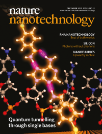
Measuring the physical properties of the bases in DNA molecules as they pass through a nanopore could form the basis of a new approach for sequencing DNA. Theorists have predicted that the quantum tunnelling of electrons can be used to identify bases, and experimenters have confirmed that tunnelling can be used to sense individual bases attached to a sugar (or a sugar and one or more phosphate groups). Now Stuart Lindsay and co-workers have shown that tunnelling from the tip of a scanning tunnelling microscope to a gold surface can be used to distinguish between different bases in the region between them. Combining such a recognition junction with a method for pulling DNA molecules through a nanopore in a controlled manner would allow researchers to read tens of bases per second. This illustration shows a single adenine base being read as it is bound by recognition molecules on the tip and surface to complete a chemical tunnelling circuit.
Image credit: Hao Liu
Letter p868; News & Views p828
-
No. 11 November 2010
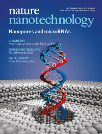
Small RNA molecules, called microRNAs, are important in various areas of biology but many of the methods used to detect them are time consuming or prone to error. Now Marija Drndić and co-workers have developed an electronic method for detecting picogram levels of rat liver microRNA. Collecting and analysing the microRNA from living tissue is a three-step process: first, an RNA probe complementary to the target microRNA sequence is added to the sample; next, the probe:microRNA duplex is enriched through binding to a viral protein; lastly, the abundance of the duplex is quantified using a nanopore. The performance of the detection system is improved by reducing the thickness of the membrane containing the nanopore and reducing the diameter of the nanopore itself.
Image credit: Robert R. Johnson
Article p807
-
No. 10 October 2010
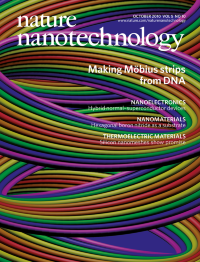
The Möbius strip is a classic example of a topological structure. It can be made by taking a strip of paper, giving it a half twist and then joining the ends together to form a loop with only one side and one edge. Cutting lengthways along the centre destroys the Möbius strip, creating a loop that contains two twists and is twice as long as the original. Cutting lengthways along a line one-third of the width in from the edge creates a thinner Möbius strip interlocked with a longer loop that contains two twists. Now, researchers at Arizona State University have used DNA origami to assemble a nanoscale version of a Möbius strip and shown that it can be cut to form new structures as described above. The strips are ~210 nm long and contain 11 DNA double helices (shown in different colours in this illustration).
Cover design by Karen Moore
Letter p712
-
No. 9 September 2010
The lateral feature resolution in conventional far-field optical lithography is diffraction-limited, and although methods have been developed to beat this limit, they can be difficult to implement and/or are limited in the range of patterns they can produce. Chad Mirkin and co-workers have now shown that a combination of nearfield scanning optical microscopy and polymer-pen lithography — a technique based on scanning probe microscopy — can overcome these problems. In this new approach, which is called beam-pen lithography, light is passed through nanoscale apertures at the end of each tip in a two-dimensional array of pyramid-shaped 'pens', allowing large areas to be patterned with high throughput. The cover shows an optical microscopy image of a representative region of ~15,000 duplicate photoresist patterns of a Chicago skyline. The entire cover image is about 300 micrometres across.
Letter p637; News & Views p629
-
No. 8 August 2010
The outstanding properties of graphene make it attractive for applications in flexible electronics. But efforts to make transparent conducting films have been hampered by the lack of efficient methods for the synthesis, transfer and doping of graphene at the scale and quality required for such applications. Now Byung Hee Hong, Jong-Hyun Ahn and co-workers have demonstrated roll-to-roll production and wet chemical doping of mostly monolayer graphene films grown by chemical vapour deposition onto flexible copper substrates. They also used layer-by-layer stacking to fabricate a doped four-layer film with properties superior to those of commercial transparent electrodes such as indium tin oxides. The photograph on the cover shows a flexible touch-screen device containing graphene electrodes.
Photograph by Ji Hye Hong and Min Young Kim
Letter p574; News & Views p559
-
No. 7 July 2010
The brightest colours in nature arise from the interaction of light with surfaces that exhibit periodic structure on the micro and nanoscales. In the wings of butterflies, for example, a combination of multilayer interference, optical gratings, photonic crystals and other optical structures gives rise to complex colour mixing, but it remains a challenge to create artificial replicas of natural photonic structures. Now Ulrich Steiner, Jeremy Baumberg and co-workers have used a combination of growth processes — including self-assembly, sputtering and atomic-layer deposition — to fabricate photonic structures that mimic the colour-mixing effect found on the wings of the Papilio blumei butterfly, and to make new structures that display enhanced optical properties. The background image is an optical micrograph of a scale taken from a butterfly wing.
Cover design by Karen Moore
Letter p511
-
No. 6 June 2010
The epitaxial growth of germanium on silicon leads to the selfassembly of SiGe nanocrystals with well-defined properties. Silvano De Franceschi and co-workers have now attached aluminium electrodes to individual nanocrystals to study the behaviour of holes in this system. They also make a hybrid superconductor-semiconductor device called a resonant supercurrent transistor by cooling their device below the superconducting transition temperature of aluminium. The cover shows d2 I/dV 2 as a function of the applied bias voltage V (vertical axis) and magnetic field (horizontal axis), where I is the current carried by the holes; high positive values of d2 I/dV 2 are shown in red, and low negative values in green. The oval structure in the middle is due to the opening of a superconducting gap in the aluminium contacts for values of the magnetic field around zero.
Cover design by Karen Moore
Article p458
-
No. 5 May 2010
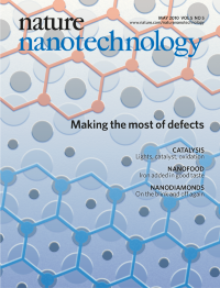
Most electronic devices contain dopant atoms that have been introduced to modify the electronic properties of the device. Graphene â a single layer of carbon atoms bonded together in a hexagonal lattice â is being explored as a material for next-generation devices, but it is difficult to dope graphene at the nanoscale using traditional doping techniques. An alternative is to create defects in the hexagonal lattice by moving and removing carbon atoms in a process called 'self-doping'. Now Matthias Batzill and co-workers have used this approach to produce an extended one-dimensional defect that acts as a metallic wire embedded in an otherwise perfect graphene sheet on a nickel surface. The defect forms between domains (shown here in pale red and blue) in which the carbon atoms rest in hollows that are either one or two nickel layers deep.
Cover design by Karen Moore
Letter p326; News & Views p316
-
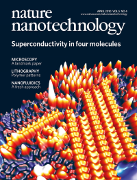
No. 4 April 2010
Superconductivity is a macroscopic quantum phenomenon that occurs when a material is cooled below a critical transition temperature. Much research has focused on increasing this transition temperature and making longer superconducting wires for applications. But how small can a sample of superconducting material be and still display superconductivity? To address this question Saw-Wai Hla and co-workers deposited (BETS)2GaCl4 molecules on a silver surface and used scanning tunnelling spectroscopy to examine the molecular islands and chains that formed. They observed a superconducting gap below about 10 K. Moreover, the size of the gap depended on the length of the chains and could still be seen in chains that contained just four molecules. In this scanning tunnelling microscope image, which measures 18.5 nm across, the silver surface is mostly blue/purple and six chains of molecules (orange) can be seen.
Cover design by Karen Moore
Letter p261; News & Views p244
-
No. 3 March 2010
Light sources that can emit just one photon at a time are needed for many applications in nanophotonics and beyond. A number of single-photon sources have been demonstrated, but none of these have combined a high flux of single photons with stable operation at room temperature. Nitrogen-vacancy centres in diamond are a promising alternative, but luminescent centres in bulk diamond crystals have the disadvantage of low photon out-coupling. Now Marko Lončar and co-workers have demonstrated a single-photon source composed of a nitrogen-vacancy centre in a diamond nanowire, which produces ten times greater flux than bulk diamond devices, while using ten times less power. The schematic on the cover shows an array of these nanowires, which typically have diameters of around 200 nm and lengths of about 2 âμm.
Cover design by Karen Moore
Letter p195
-
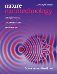
No. 2 February 2010
Single-molecule fluorescence spectroscopy has allowed many chemical and biological systems to be studied both in vitro and in vivo. However, it is difficult to perform such measurements at temperatures above 37â°C because the index-matching fluids used to direct light from the sample to the lens can also conduct heat, and this heating can damage the lens. Now Jerrod Schwartz, Stavros Stavrakis and Stephen Quake have shown that a colloidal titanium dioxide particle can act as a microlens when placed next to an emitting molecule. This microlens focuses light from the molecule into a conventional lens that is separated from the sample by air, which allows single-molecule measurements to be performed on biological systems in real time at temperatures as high as 70â°C. This image is based on a simulation showing how light from a point source is focused by the microlens.
Cover design by Karen Moore
Letter p127; News & Views p99
-
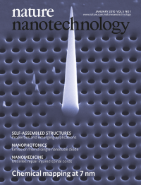
No. 1 January 2010
The fields of plasmonics, Raman spectroscopy and atomic force microscopy have experienced a number of significant, but largely unrelated, advances in recent years. Now Enzo Di Fabrizio and co-workers have made a photonic-plasmonic device that is fully compatible with atomic force microscopy and Raman spectroscopy, and used it to obtain topographic, chemical and structural information on silicon nanocrystals with a spatial resolution of 7 nm. Their approach relies on generating surface plasmon polaritons that are compressed as they travel along a silver tapered waveguide to create strongly enhanced Raman excitation in a region just a few nanometres across. This scanning electron microscope image shows the plasmonic waveguide sitting on a silicon nitride membrane containing a two-dimensional photonic crystal cavity. The apex of the waveguide has a radius of curvature less than 5 nm.
Cover design by Karen Moore
Letter p67; News & Views p10