Volume 4
-
No. 12 December 2009
Researchers are able to control many of the properties of semiconductor nanowires including their composition, doping, crystal structure and orphology. However, progress towards the ab initio design and growth of hierarchical nanostructures has been limited. Now Charles Lieber and co-workers have demonstrated a 'nanotectonic' approach that provides iterative control over the nucleation and growth of nanowires, and they have used this approach to grow kinked or zigzag nanowires in which straight sections of controllable length are separated by triangular joints. Moreover, the growth direction remains coherent along the nanowire. They have also grown nanowires with specific device functions, such as p-n diodes and field-effect transistors, localized at the kinked junctions. The image on the cover is a composite of the same false-colour scanning electron microscope image of a single multiply-kinked nanowire with a diameter of 80 nm and a segment length of 1 âμm.
Image credit: B. Tian and C. Lieber.
Letter p824
Focus
-
No. 11 November 2009
It is known that lattice strain can cause the coexistence of metallic and insulating phases in vanadium dioxide. Now Junqiao Wu and co-workers have shown that strain can also produce ordered arrays of these phases in single-crystal beams of vanadium dioxide. In particular they are able to lower the temperature of the Mott transition between the insulating and metallic phases from its bulk value of 341 K to room temperature. The optical microscope images on the cover show (from left to right) a nanobeam in a pure insulating phase at 298 K, the same beam in a pure metallic phase at 343 K, and the effect of bending this beam at five different positions with a tungsten needle (343 K). The arrays of insulating (bright) and metallic (dark) phases can be clearly seen.
(Image credit: Jinbo Cao).
Letter p732
-
No. 10 October 2009
π-conjugated molecules can self-assemble into quasi-one-dimensional nanostructures with intriguing optoelectronic properties. However, many potential applications require these nanostructures to be immobilized on a solid substrate, which is difficult to do without damaging them. David Vanden Bout and co-workers have now immobilized double-walled molecular nanotubes made from cyanine dyes, demonstrating that they remain morphologically intact and also display highly uniform optical properties. The thin yellow lines in this image from a scanning force microscope are single cyanine-dye nanotubes and the thicker lines are bundles of such nanotubes; the image is 10 μm across.
Cover design by Karen Moore
Letter p658; Editorial p607
Focus
-
No. 9 September 2009
DNA origami - the folding of long single strands of DNA into predetermined shapes using shorter 'staple strands' - can create nanostructures on which other species, such as nanoparticles, can be bound. However, DNA origami are synthesized in solution and uncontrolled deposition results in random arrangements of the nanostructures on surfaces. A team of researchers from IBM Research Almaden and the California Institute of Technology now report the placement of DNA origami shapes on lithographically patterned surfaces. From solution, DNA triangles with edges of 127 nm can bind accurately to shape-matched sites on a surface. Larger surface templates can also be used, and the atomic force microscopy image on the cover shows the triangles placed in 500-nm-wide lines patterned on a diamond-like carbon surface.
Cover design by Karen Moore
Letter p557; News & Views p543
-
No. 8 August 2009
Numerous attempts have been made to sequence single molecules of DNA with a scanning tunnelling microscope (STM) but there have been problems with preparing samples and reproducing results. Now, Hiroyuki Tanaka and Tomoji Kawai report a method for depositing single DNA molecules on a copper surface and go on to determine the 'electronic fingerprint' for guanine — one of the four bases found in DNA molecules. Their results show that it is possible to sequence individual guanine bases in real long-chain DNA molecules with high-resolution STM imaging and scanning tunnelling spectroscopy. The false-colour STM image on the cover, which measures 67 nm across, shows a DNA molecule running from bottom left to top right.
Cover design by Karen Moore
Letter p518; News & Views p476
-
No. 7 July 2009
Many strongly correlated electron systems have a domain structure that obscures the fundamental properties of the material. Nanoscale samples, on the other hand, can be smaller than the characteristic domain size, thus making it possible to explore these fundamental properties in detail. Experiments by David Cobden and co-workers on single-domain nanobeams made of vanadium dioxide have revealed several new aspects of the metal-insulator transition in this material, including supercooling of the metallic phase, and a connection between the transition and the equilibrium carrier density in the insulating phase. The cover image, 85 m across, shows vanadium dioxide crystals and nanobeams attached to a silica substrate at 70 °C: the stripes are alternating metallic (darker) and insulating regions.
Cover design by Karen Moore
Letter p420; News & Views p406
-
No. 6 June 2009
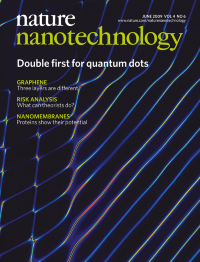
Quantum dots defined in carbon nanotubes are attractive for exploring a wide range of phenomena in fundamental physics. For some of these experiments it is necessary to confine a single electron in a quantum dot, while controlling the height of the barriers on either side of the dot, but this has proved difficult. Now, Gary Steele, Georg Gotz and Leo Kouwenhoven have confined a single electron in a tunable double quantum dot in a nanotube for the first time, and also observed a novel type of tunnelling that is analogous to relativistic Klein tunnelling. This false-colour plot shows electric current as a function of the voltages applied to two of the gates in the system.
Letter p363; News & Views p347
-
No. 5 May 2009
Force spectroscopy allows the measurement of reaction rates as a function of the restoring force in molecules that have been stretched or compressed, but it lacks the temporal and spatial resolution needed to study small functional groups. A molecular force probe that extends force spectroscopy to the size-scale of such reactions has now been reported by roman Boulatov and co-workers. This artist's impression shows how stiff stillbene molecules can be used to apply forces to a small functional group: the stiff stilbene molecule changes shape when it is exposed to certain wavelengths of light, and this changes the force experienced by the smaller molecule.
Image credit: Marina Bulan
Letter p302; News & Views p284; Editorial p271
-
No. 4 April 2009
The ability of DNA to self-assemble into a variety of nanostructures and nanomachines is being exploited by a growing number of researchers. Itamar Willner and co-workers have demonstrated the power of DNA nanotechnology by making DNA scaffolds that contain 'hinges' to which biomolecules such as enzymes can be tethered. They go on to show that enzyme cascades can proceed effectively on these scaffolds. The artist's impression on the cover shows two such enzymes - glucose oxidase (GOX) and horseradish peroxidase (HRP) - on a hexagonal DNA scaffold that is about 33-nm wide. Cascades are not observed when these two enzymes are mixed in solution.
Cover design by Karen Moore
Letter p249; News & Views p211; Editorial p203
-
No. 3 March 2009
The potential of nanotechnology was famously demonstrated in 1990 when researchers used a scanning tunnelling microscope (STM) to spell out IBM with 35 xenon atoms on a nickel surface. It was thought that the need to have enough distance between the atoms or molecules to stop them reacting with each other would limit the amount of information that could be written on a surface. Hari Manoharan and co-workers now show that it is possible to exceed this limit with quantum holography. The information is encoded into the wavefunctions of a two-dimensional electron gas using holograms constructed from single molecules, and is read with a STM. This STM spectral image (1.3 nm across) reveals the letter 'S' comprised of 0.3 nm bits.
Cover design by Karen Moore
Article p167; News & Views p141
-
No. 2 February 2009
Research into public perceptions of nanotechnology is becoming more rigorous with social scientists developing and testing increasingly complex theoretical models, as demonstrated by three papers in this issue. Dan Kahan and coworkers investigated the influence of cultural factors - in particular, whether individuals were pro- or anti-commerce - on attitudes towards the risks and benefits associated with nanotechnology; Dietram Scheufele and colleagues combined the results of public surveys in the US and Europe to explore the influence of religious beliefs on public perceptions of nanotechnology. In the third study Nick Pidgeon and co-workers found that energy applications of nanotechnology were viewed more positively than health applications in workshops organized in the UK and the US. (Image credit: Dariusz Miszkiel/123RF.)
Cover design by Karen Moore
Letters p87, 91 and 95; News & Views p79; Editorial p71
-
No. 1 January 2009
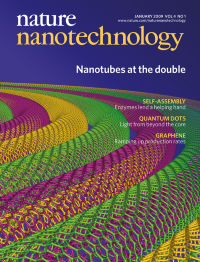
Double-walled carbon nanotubes are ideal systems for studying the interwall interactions that influence the properties of nanotubes with two or more walls. However, current synthesis techniques produce unwanted single- and multi-walled nanotubes. Alexander Green and Mark Hersam have now shown that density-gradient ultracentrifugation can be used to separate doublewalled nanotubes from mixtures of single- and multi-walled nanotubes. The cover image is a schematic representation showing the atomic structure of an array of double-walled nanotubes; the diameter of each nanotube is approximately 2 nm.
Cover design by Karen Moore
Article p64

