Thank you for visiting nature.com. You are using a browser version with limited support for CSS. To obtain
the best experience, we recommend you use a more up to date browser (or turn off compatibility mode in
Internet Explorer). In the meantime, to ensure continued support, we are displaying the site without styles
and JavaScript.
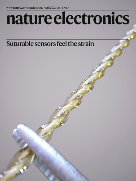
Stretchable sensors that are made from two conductive fibres in a double helical structure and with a hollow core can be directly sutured to connective tissues to wirelessly monitor strain. The computer-generated image on the cover illustrates a stretchable strain sensor with a double helical turn density of three turns per centimetre and a hollow core diameter of 500 micrometres.
Through a combination of talent cultivation and innovative research and development, the integrated circuit design industry in Taiwan now plays a central role in global electronics.
Woven displays with a high number of light-emitting pixels can be created by interlacing two electrically conducting fibres and forming electroluminescent units at the crossover points.
Transistors that are printed on paper substrates using all-carbon inks can be completely recycled, providing a potential route to helping solve the problem of electronic waste.
This Review examines the development of radiation-hardened electronics, considering the design methodologies available with conventional complementary metal–oxide–semiconductor (CMOS) technologies and the potential use and applications of emerging memory technologies.
An electric-field-induced reversible hydrogenation reaction, which relies on a hydrogen-ion electrolyte, can be used to create graphene field-effect transistors with on/off current ratios of 108 and endurance of up to 1 million switching cycles.
All-carbon thin-film transistors—made using crystalline nanocellulose as a dielectric, carbon nanotubes as a semiconductor and graphene as a conductor—can be printed onto paper substrates and the constituent materials subsequently recycled.
Twisted trilayer structures of anisotropic black phosphorus can be used to create resonant tunnelling diodes in which the twist angle between the layers can be used to control the vertical transport behaviour.
Bilayer beta tellurium dioxide nanosheets with p-type characteristics can be formed through the surface oxidation of a mixture of tellurium and selenium, and used to create transistors with performance that matches their n-type oxide counterparts.
AlGaN/GaN nanowires containing multiple two-dimensional electron gas channels can be used to create tri-gate power transistors that overcome trade-offs between carried density and mobility.
A capacitive, fibre-like stretchable strain sensor, formed of two conductors in a double helical structure, can be combined with an inductive coil to create a wireless strain-sensing system for biomedical applications.
A wearable platform, which uses a thermal sensing module isolated from biofluids and a Bluetooth Low Energy system on a chip for wireless data transfer, can be used to continuously monitor sweat.