Abstract
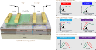
The co-integration of logic switches and neuromorphic functions could be used to create new computing architectures with low power consumption and novel functionalities. Two-dimensional (2D) semiconductors and ferroelectric materials could be potentially used to make such devices, but integrating them on the same platform is challenging. Here we show that the 2D semiconductor tungsten diselenide and 2D/2D heterostructures of tungsten diselenide/tin diselenide can be integrated with doped high-k ferroelectric (silicon-doped hafnium oxide) and high-k dielectric gate stacks. With this single platform, four types of logic switch—2D metal–oxide–semiconductor field-effect transistors (FETs), 2D/2D tunnel FETs, negative-capacitance 2D FETs and negative-capacitance 2D/2D tunnel FETs—can be created. The negative-capacitance tungsten diselenide/tin diselenide tunnel FET exhibits an average subthreshold swing of 55 mV dec–1 over four decades of current, and the negative-capacitance tungsten diselenide FET exhibits an average subthreshold swing of 50 mV dec–1 over three decades. The shared ferroelectric gate stacks on 2D devices can also be exploited to create co-integrated artificial synapses for neuromorphic computing.
This is a preview of subscription content, access via your institution
Access options
Access Nature and 54 other Nature Portfolio journals
Get Nature+, our best-value online-access subscription
$29.99 / 30 days
cancel any time
Subscribe to this journal
Receive 12 digital issues and online access to articles
$119.00 per year
only $9.92 per issue
Buy this article
- Purchase on Springer Link
- Instant access to full article PDF
Prices may be subject to local taxes which are calculated during checkout


Data availability
The data that support the findings of this study are available from the corresponding author upon reasonable request.
References
Ionescu, A. M. Energy efficient computing and sensing in the zettabyte era: from silicon to the cloud. In 2017 IEEE International Electron Devices Meeting (IEDM) 1–2 (IEEE, 2017).
Mutlu, O., Ghose, S., Gómez-Luna, J. & Ausavarungnirun, R. Processing data where it makes sense: enabling in-memory computation. Microprocess. Microsyst. 67, 28–41 (2019).
Waldrop, M. M. The chips are down for Moore’s law. Nat. N. 530, 144 (2016).
Liu, C. et al. Small footprint transistor architecture for photoswitching logic and in situ memory. Nat. Nanotechnol. 14, 662–667 (2019).
Zhang, Z. et al. All-in-one two-dimensional retinomorphic hardware device for motion detection and recognition. Nat. Nanotechnol. 17, 27–32 (2022).
Qiu, C. et al. Dirac-source field-effect transistors as energy-efficient, high-performance electronic switches. Science 361, 387–392 (2018).
Zhang, W. et al. Neuro-inspired computing chips. Nat. Electron. 3, 371–382 (2020).
Franklin, A. D. Nanomaterials in transistors: from high-performance to thin-film applications. Science 349, aab2750 (2015).
Ionescu, A. Beyond CMOS: steep-slope devices and energy efficient nanoelectronics. in High Mobility Materials for CMOS Applications 281–305 (Elsevier, 2018).
Convertino, C. et al. A hybrid III–V tunnel FET and MOSFET technology platform integrated on silicon. Nat. Electron. 4, 162–170 (2021).
Han, J.-K. et al. Cointegration of single-transistor neurons and synapses by nanoscale CMOS fabrication for highly scalable neuromorphic hardware. Sci. Adv. 7, eabg8836 (2021).
Orji, N. G. et al. Metrology for the next generation of semiconductor devices. Nat. Electron. 1, 532–547 (2018).
Tong, L. et al. 2D materials–based homogeneous transistor-memory architecture for neuromorphic hardware. Science 373, 1353–1358 (2021).
Sebastian, A., Le Gallo, M., Khaddam-Aljameh, R. & Eleftheriou, E. Memory devices and applications for in-memory computing. Nat. Nanotechnol. 15, 529–544 (2020).
Raitza, M. et al. Exploiting transistor-level reconfiguration to optimize combinational circuits. In Design, Automation & Test in Europe Conference & Exhibition (DATE), 2017 338–343 (IEEE, 2017).
Yan, H. et al. Programmable nanowire circuits for nanoprocessors. Nature 470, 240–244 (2011).
Liu, Y., Huang, Y. & Duan, X. Van der Waals integration before and beyond two-dimensional materials. Nature 567, 323–333 (2019).
Liu, Y. et al. Promises and prospects of two-dimensional transistors. Nature 591, 43–53 (2021).
Wu, P., Reis, D., Hu, X. S. & Appenzeller, J. Two-dimensional transistors with reconfigurable polarities for secure circuits. Nat. Electron. 4, 45–53 (2021).
Sun, X. et al. Reconfigurable logic-in-memory architectures based on a two-dimensional van der Waals heterostructure device. Nat. Electron. 5, 752–760 (2022).
Pan, C. et al. Reconfigurable logic and neuromorphic circuits based on electrically tunable two-dimensional homojunctions. Nat. Electron. 3, 383–390 (2020).
Yan, X. et al. Tunable SnSe2/WSe2 heterostructure tunneling field effect transistor. Small 13, 1701478 (2017).
Oliva, N. et al. WSe2/SnSe2 vdW heterojunction tunnel FET with subthermionic characteristic and MOSFET co-integrated on same WSe2 flake. npj 2D Mater. Appl. 4, 5 (2020).
Kamaei, S. et al. Gate energy efficiency and negative capacitance in ferroelectric 2D/2D TFET from cryogenic to high temperatures. npj 2D Mater. Appl. 5, 76 (2021).
Saripalli, V., Mishra, A., Datta, S. & Narayanan, V. An energy-efficient heterogeneous CMP based on hybrid TFET-CMOS cores. In Proc. 48th Design Automation Conference 729–734 (ACM, 2011).
Fan, S. et al. Tunable negative differential resistance in van der Waals heterostructures at room temperature by tailoring the interface. ACS Nano 13, 8193–8201 (2019).
Salahuddin, S. & Datta, S. Use of negative capacitance to provide voltage amplification for low power nanoscale devices. Nano Lett. 8, 405–410 (2008).
Ionescu, A. M. Negative capacitance gives a positive boost. Nat. Nanotechnol. 13, 7–8 (2018).
Kim, S. et al. Ferroelectric polymer-based artificial synapse for neuromorphic computing. Nanoscale Horiz. 6, 139–147 (2021).
Tian, B. et al. A robust artificial synapse based on organic ferroelectric polymer. Adv. Electron. Mater. 5, 1800600 (2019).
Chen, Y. et al. Graphene–ferroelectric transistors as complementary synapses for supervised learning in spiking neural network. npj 2D Mater. Appl. 3, 31 (2019).
Salahuddin, S. & Datta, S. Can the subthreshold swing in a classical FET be lowered below 60 mV/decade? In 2008 IEEE International Electron Devices Meeting 1–4 (IEEE, 2008).
Mulaosmanovic, H. et al. Novel ferroelectric FET based synapse for neuromorphic systems. In 2017 Symposium on VLSI Technology T176–T177 (IEEE, 2017).
Gupta, N., Makosiej, A., Vladimirescu, A., Amara, A. & Anghel, C. 3T-TFET bitcell based TFET-CMOS hybrid SRAM design for ultra-low power applications. In 2016 Design, Automation & Test in Europe Conference & Exhibition (DATE) 361–366 (IEEE, 2016).
Strangio, S. et al. Digital and analog TFET circuits: sesign and benchmark. Solid-State Electron. 146, 50–65 (2018).
Fulde, M. et al. Fabrication, optimization and application of complementary multiple-gate tunneling FETs. In 2008 2nd IEEE International Nanoelectronics Conference 579–584 (IEEE, 2008).
Resta, G. V. et al. Polarity control in WSe2 double-gate transistors. Sci. Rep. 6, 29448 (2016).
Sarkar, D. et al. A subthermionic tunnel field-effect transistor with an atomically thin channel. Nature 526, 91–95 (2015).
Tomioka, K., Yoshimura, M. & Fukui, T. Steep-slope tunnel field-effect transistors using III–V nanowire/Si heterojunction. In 2012 Symposium on VLSI Technology (VLSIT) 47–48 (IEEE, 2012).
Li, W., Xiao, X. & Xu, H. Versatile electronic devices based on WSe2/SnSe2 vertical van der Waals heterostructures. ACS Appl. Mater. Interfaces 11, 30045–30052 (2019).
Si, M. et al. Steep-slope hysteresis-free negative capacitance MoS2 transistors. Nat. Nanotechnol. 13, 24–28 (2018).
Tosun, M. et al. High-gain inverters based on WSe2 complementary field-effect transistors. ACS Nano 8, 4948–4953 (2014).
Saeidi, A., Jazaeri, F., Stolichnov, I., Enz, C. C. & Ionescu, A. M. Negative capacitance as universal digital and analog performance booster for complementary MOS transistors. Sci. Rep. 9, 9105 (2019).
Rusu, A., Saeidi, A. & Ionescu, A. M. Condition for the negative capacitance effect in metal–ferroelectric–insulator–semiconductor devices. Nanotechnology 27, 115201 (2016).
Zhu, Z. et al. Negative-capacitance characteristics in a steady-state ferroelectric capacitor made of parallel domains. IEEE Electron Device Lett. 38, 1176–1179 (2017).
Lu, H. & Seabaugh, A. Tunnel field-effect transistors: state-of-the-art. IEEE J. Electron Devices Soc. 2, 44–49 (2014).
Saeidi, A. et al. Nanowire tunnel FET with simultaneously reduced subthermionic subthreshold swing and off-current due to negative capacitance and voltage pinning effects. Nano Lett. 20, 3255–3262 (2020).
Bayat, F. M. et al. Implementation of multilayer perceptron network with highly uniform passive memristive crossbar circuits. Nat. Commun. 9, 2331 (2018).
Adam, G. C., Khiat, A. & Prodromakis, T. Challenges hindering memristive neuromorphic hardware from going mainstream. Nat. Commun. 9, 5267 (2018).
Yang, J.-T. et al. Artificial synapses emulated by an electrolyte-gated tungsten-oxide transistor. Adv. Mater. 30, 1801548 (2018).
Yang, C. S. et al. A synaptic transistor based on quasi-2D molybdenum oxide. Adv. Mater. 29, 1700906 (2017).
Gastaldi, C. et al. Intrinsic switching in Si-doped HfO2: a study of Curie–Weiss law and its implications for negative capacitance field-effect transistor. Appl. Phys. Lett. 118, 192904 (2021).
Gokmen, T. & Vlasov, Y. Acceleration of deep neural network training with resistive cross-point devices: design considerations. Front. Neurosci. 10, 333 (2016).
Yu, S. et al. Scaling-up resistive synaptic arrays for neuro-inspired architecture: challenges and prospect. In 2015 IEEE International Electron Devices Meeting (IEDM) 17.3.1–17.3.4 (IEEE, 2015).
Nishitani, Y., Kaneko, Y., Ueda, M., Morie, T. & Fujii, E. Three-terminal ferroelectric synapse device with concurrent learning function for artificial neural networks. J. Appl. Phys. 111, 124108 (2012).
Sanchez Esqueda, I. et al. Aligned carbon nanotube synaptic transistors for large-scale neuromorphic computing. ACS Nano 12, 7352–7361 (2018).
Seo, S. et al. Artificial van der Waals hybrid synapse and its application to acoustic pattern recognition. Nat. Commun. 11, 3936 (2020).
Halter, M. et al. Back-end, CMOS-compatible ferroelectric field-effect transistor for synaptic weights. ACS Appl. Mater. Interfaces 12, 17725–17732 (2020).
Quellmalz, A. et al. Large-area integration of two-dimensional materials and their heterostructures by wafer bonding. Nat. Commun. 12, 917 (2021).
Liu, C. et al. Two-dimensional materials for next-generation computing technologies. Nat. Nanotechnol. 15, 545–557 (2020).
Yang, T. et al. Van der Waals epitaxial growth and optoelectronics of large-scale WSe2/SnS2 vertical bilayer p–n junctions. Nat. Commun. 8, 1906 (2017).
Gandhi, R. et al. CMOS-compatible vertical-silicon-nanowire gate-all-around p-type tunneling FETs with ≤50-mV/decade subthreshold swing. IEEE Electron Device Lett. https://doi.org/10.1109/LED.2011.2165331 (2011).
K. Jeon et al., Si tunnel transistors with a novel silicided source and 46mV/dec swing. In 2010 Symposium on VLSI Technology, Honolulu, HI, USA https://doi.org/10.1109/VLSIT.2010.5556195 (2010).
Leonelli, D. et al. Performance enhancement in multi gate tunneling field effect transistors by scaling the fin-width. Jpn. J. Appl. Phys. https://doi.org/10.1143/JJAP.49.04DC10 (2010).
Knoll, L. et al. Inverters with strained Si nanowire complementary tunnel field-effect transistors. IEEE Electron Device Lett. https://doi.org/10.1109/LED.2013.2258652 (2013).
Villalon, A. et al. Strained tunnel FETs with record ION: first demonstration of ETSOI TFETs with SiGe channel and RSD. In Symposium on VLSI Technology (VLSIT), Honolulu, HI, USA https://doi.org/10.1109/VLSIT.2012.6242455 (2012).
Acknowledgements
Author information
Authors and Affiliations
Contributions
S.K. and A.M.I. conceived the main idea of this experimental study and designed and developed the process flow. S.K., X.L. and J.B. conceived the fabrication process. S.K. performed the electrical measurements and data analysis. C.G. performed the atomic force microscopy and piezoelectric force microscopy measurements. S.K., C.G. and A.S. carried out the MFM characterization and optimization. S.K. and Y.W. performed the pulsed measurements. S.K. and A.S. prepared the figures and schematics. S.K., A.S., J.B. and A.M.I. wrote the manuscript.
Corresponding author
Ethics declarations
Competing interests
The authors declare no competing interests.
Peer review
Peer review information
Nature Electronics thanks Zheng-Dong Luo, Shubhadeep Bhattacharjee and the other, anonymous, reviewer(s) for their contribution to the peer review of this work.
Additional information
Publisher’s note Springer Nature remains neutral with regard to jurisdictional claims in published maps and institutional affiliations.
Supplementary information
Supplementary Information
Supplementary Notes 1–5, Figs. 1–24 and Tables 1 and 2.
Rights and permissions
Springer Nature or its licensor (e.g. a society or other partner) holds exclusive rights to this article under a publishing agreement with the author(s) or other rightsholder(s); author self-archiving of the accepted manuscript version of this article is solely governed by the terms of such publishing agreement and applicable law.
About this article
Cite this article
Kamaei, S., Liu, X., Saeidi, A. et al. Ferroelectric gating of two-dimensional semiconductors for the integration of steep-slope logic and neuromorphic devices. Nat Electron 6, 658–668 (2023). https://doi.org/10.1038/s41928-023-01018-7
Received:
Accepted:
Published:
Issue Date:
DOI: https://doi.org/10.1038/s41928-023-01018-7
This article is cited by
-
Realization of sextuple polarization states and interstate switching in antiferroelectric CuInP2S6
Nature Communications (2024)
-
A reconfigurable single-gate transistor
Nature Electronics (2023)
-
Ferroelectrics meet transition metal dichalcogenides
Nature Reviews Materials (2023)


