Abstract
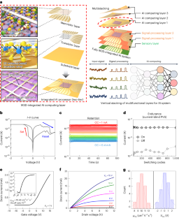
Three-dimensional (3D) hetero-integration technology is poised to revolutionize the field of electronics by stacking functional layers vertically, thereby creating novel 3D circuity architectures with high integration density and unparalleled multifunctionality. However, the conventional 3D integration technique involves complex wafer processing and intricate interlayer wiring. Here we demonstrate monolithic 3D integration of two-dimensional, material-based artificial intelligence (AI)-processing hardware with ultimate integrability and multifunctionality. A total of six layers of transistor and memristor arrays were vertically integrated into a 3D nanosystem to perform AI tasks, by peeling and stacking of AI processing layers made from bottom-up synthesized two-dimensional materials. This fully monolithic-3D-integrated AI system substantially reduces processing time, voltage drops, latency and footprint due to its densely packed AI processing layers with dense interlayer connectivity. The successful demonstration of this monolithic-3D-integrated AI system will not only provide a material-level solution for hetero-integration of electronics, but also pave the way for unprecedented multifunctional computing hardware with ultimate parallelism.
This is a preview of subscription content, access via your institution
Access options
Access Nature and 54 other Nature Portfolio journals
Get Nature+, our best-value online-access subscription
$29.99 / 30 days
cancel any time
Subscribe to this journal
Receive 12 print issues and online access
$259.00 per year
only $21.58 per issue
Buy this article
- Purchase on Springer Link
- Instant access to full article PDF
Prices may be subject to local taxes which are calculated during checkout


Data availability
All data are available in the main text or Supplementary Information. All relevant data are available from the corresponding authors upon reasonable request.
References
Saleh, R. et al. System-on-chip: reuse and integration. Proc. IEEE 94, 1050–1069 (2006).
Wolf, W., Jerraya, A. A. & Martin, G. Multiprocessor system-on-chip (MPSoC) technology. IEEE Trans. Comput. Aided Des. Integr. Circuits Syst. 27, 1701–1713 (2008).
Patti, R. S. Three-dimensional integrated circuits and the future of system-on-chip designs. Proc. IEEE 94, 1214–1224 (2006).
Shulaker, M. M. et al. Three-dimensional integration of nanotechnologies for computing and data storage on a single chip. Nature 547, 74–78 (2017).
Choi, C. et al. Reconfigurable heterogeneous integration using stackable chips with embedded artificial intelligence. Nat. Electron. 5, 386–393 (2022).
Lin, P. et al. Three-dimensional memristor circuits as complex neural networks. Nat. Electron. 3, 225–232 (2020).
Zhou, F. et al. Optoelectronic resistive random access memory for neuromorphic vision sensors. Nat. Nanotechnol. 14, 776–782 (2019).
Mennel, L. et al. Ultrafast machine vision with 2D material neural network image sensors. Nature 579, 62–66 (2020).
Tu, K.-N. Reliability challenges in 3D IC packaging technology. Microelectron. Reliab. 51, 517–523 (2011).
Lau, J. H. Evolution, challenge, and outlook of TSV, 3D IC integration and 3D silicon integration. In 2011 International Symposium on Advanced Packaging Materials (APM), 462–488 (IEEE, 2011).
Shulaker, M. M. et al. Monolithic 3D integration: a path from concept to reality. In 2015 Design, Automation & Test in Europe Conference & Exhibition (DATE) 1197–1202 (IEEE, 2015).
Wong, S. et al. Monolithic 3D integrated circuits. In 2007 International Symposium on VLSI Technology, Systems and Applications (VLSI-TSA) 1–4 (IEEE, 2007).
Bishop, M. D., Wong, H.-S. P., Mitra, S. & Shulaker, M. M. Monolithic 3-D integration. IEEE Micro 39, 16–27 (2019).
Liu, Y., Huang, Y. & Duan, X. Van der Waals integration before and beyond two-dimensional materials. Nature 567, 323–333 (2019).
Geim, A. K. & Grigorieva, I. V. Van der Waals heterostructures. Nature 499, 419–425 (2013).
Novoselov, K. S., Mishchenko, A., Carvalho, O. A. & Castro Neto, A. 2D materials and van der Waals heterostructures. Science 353, aac9439 (2016).
Kim, K. S. et al. Non-epitaxial single-crystal 2D material growth by geometric confinement. Nature 614, 88–94 (2023).
Li, M. et al. Imperfection-enabled memristive switching in van der Waals materials. Nat. Electron. 6, 491–505 (2023).
Yang, S., Jiang, C. & Wei, S.-H. Gas sensing in 2D materials. Appl. Phys. Rev. 4, 021304 (2017).
Long, M., Wang, P., Fang, H. & Hu, W. Progress, challenges, and opportunities for 2D material based photodetectors. Adv. Funct. Mater. 29, 1803807 (2019).
Pang, Y., Yang, Z., Yang, Y. & Ren, T. L. Wearable electronics based on 2D materials for human physiological information detection. Small 16, 1901124 (2020).
Li, T. et al. Reconfigurable, non-volatile neuromorphic photovoltaics. Nat. Nanotechnol. https://doi.org/10.1038/s41565-023-01446-8 (2023).
Song, M.-K. et al. Recent advances and future prospects for memristive materials, devices, and systems. ACS Nano 17, 11994–12039 (2023).
Shim, J. et al. Controlled crack propagation for atomic precision handling of wafer-scale two-dimensional materials. Science 362, 665–670 (2018).
Jia, X. et al. High‐performance CMOS inverter array with monolithic 3D architecture based on CVD‐grown n‐MoS2 and p‐MoTe2. Small https://doi.org/10.1002/smll.202207927 (2023).
Jayachandran, D. et al. Monolithic three-dimensional (3D) integration of two-dimensional (2D) field effect transistors. Preprint at https://doi.org/10.21203/rs.3.rs-2512945/v1 (2023).
Guan, S.-X. et al. Monolithic 3D integration of back-end compatible 2D material FET on Si FinFET. NPJ 2D Mater. Appl. 7, 9 (2023).
Wang, C.-H. et al. 3D monolithic stacked 1T1R cells using monolayer MoS2 FET and hBN RRAM fabricated at low (150 °C) temperature. In 2018 IEEE International Electron Devices Meeting (IEDM) 22.25.21–22.25.24 (IEEE, 2018).
Tang, B. et al. Wafer-scale solution-processed 2D material analog resistive memory array for memory-based computing. Nat. Commun. 13, 3037 (2022).
Kumar, D., Aluguri, R., Chand, U. & Tseng, T.-Y. Enhancement of resistive switching properties in nitride based CBRAM device by inserting an Al2O3 thin layer. Appl. Phys. Lett. 110, 203102 (2017).
Sun, T. et al. Stable resistive switching in ZnO/PVA: MoS2 nilayer memristor. Nanomaterials 12, 1977 (2022).
Tsai, T.-L., Jiang, F.-S., Ho, C.-H., Lin, C.-H. & Tseng, T.-Y. Enhanced properties in conductive-bridge resistive switching memory with oxide-nitride bilayer structure. IEEE Electron Device. Lett. 37, 1284–1287 (2016).
Wu, F. et al. Interface engineering via MoS2 insertion layer for improving resistive switching of conductive‐bridging random access memory. Adv. Electron. Mater. 5, 1800747 (2019).
Shen, P.-C. et al. Ultralow contact resistance between semimetal and monolayer semiconductors. Nature 593, 211–217 (2021).
Das, S. et al. Transistors based on two-dimensional materials for future integrated circuits. Nat. Electron. 4, 786–799 (2021).
Wang, Y. et al. Van der Waals contacts between three-dimensional metals and two-dimensional semiconductors. Nature 568, 70–74 (2019).
Kim, T.-H. et al. Multilevel switching memristor by compliance current adjustment for off-chip training of neuromorphic system. Chaos Solitons Fractals 153, 111587 (2021).
Wan, H. et al. In situ observation of compliance-current overshoot and its effect on resistive switching. IEEE Electron Device. Lett. 31, 246–248 (2010).
Zhu, J. et al. Low-thermal-budget synthesis of monolayer molybdenum disulfide for silicon back-end-of-line integration on a 200 mm platform. Nat. Nanotechnol. 18, 456–463 (2023).
Li, X. et al. Large-area two-dimensional layered hexagonal boron nitride grown on sapphire by metalorganic vapor phase epitaxy. Cryst. Growth Des. 16, 3409–3415 (2016).
Wang, Y. & Chhowalla, M. Making clean electrical contacts on 2D transition metal dichalcogenides. Nat. Rev. Phys. 4, 101–112 (2022).
Choi, M. et al. Flexible active-matrix organic light-emitting diode display enabled by MoS2 thin-film transistor. Sci. Adv. 4, eaas8721 (2018).
Acknowledgements
The team at Massachusetts Institute of Technology acknowledges support from the Korea Institute of Science and Technology (nos. 2E32260 and 2E32242). J.-H.A. acknowledges support from the National Research Foundation of Korea (no. NRF-2015R1A3A2066337). C.H. acknowledges support from the National Science Foundation (no. DMR-1921818) and SUPREME, one of seven centres in JUMP 2.0, a Semiconductor Research Corporation programme sponsored by Defense Advanced Research Projects Agency (DARPA). S.-H.B. acknowledges financial support from Washington University in St. Louis and the institute of Materials Science and Engineering for the use of instruments and staff assistance. S.-H.B. also acknowledges that this work was partially supported by Samsung Electronics Co., Ltd. (IO221219-04250-01). This work was carried out in part through the use of MIT.nano’s facilities. The authors would like to acknowledge Dr. Baoming Wang for assistance in focused ion beam (FIB) sample preparation. M.-K.S. acknowledges support from the National Research Foundation of Korea (no. NRF-2021R1A6A3A14044297). A.O. acknowledges financial support from Georgia Tech Europe in Metz-France.
Author information
Authors and Affiliations
Contributions
J.K. and S.-H.B. conceived the idea and led the research. J.-H.K., S.-H.B. and J.K. designed experiments. J.-H.K., H.S., K.S.K., M.-K.S., J.-H.A., S.-H.B. and J.K. prepared the manuscript. H.S., A.T.H., K.S.K., D.L., R.Y. and G.Z. grew 2D thin films. P.V., S. Sundaram and A.O. worked on the growth of h-BN on sapphire. J.-H.K., H.S. and M.-K.S. performed device fabrication. H.S., J.-H.K., Y.M. and C.C. designed and conducted computing simulations. B.K., H.K., J.C., B.-I.P., J.S., J.S.K., S.H., Sangho Lee, B.K., Seungju Seo and Seunghwan Seo conducted film transfer and characterization. K.R. and E.P. conducted STEM measurements. D.L., Y.M., J.M.S., B.J.K., S.L., S.O.K., S.M., M.-C.P., S.L., H.-J.K., G.Z., S. Sundaram, A.T.H., Z.X., R.Y., H.A., H.S.K., P.L., C.H., A.O. and J.-H.A. provided feedback throughout the experiments and data analysis. The manuscript was written by J.-H.K., S.-H.B. and J.K. with input from all authors. All authors contributed to the analysis and discussion of the results leading to the manuscript.
Corresponding authors
Ethics declarations
Competing interests
The authors declare no competing interests.
Peer review
Peer review information
Nature Materials thanks Weida Hu, Tianyou Zhai and Ilia Valov for their contribution to the peer review of this work.
Additional information
Publisher’s note Springer Nature remains neutral with regard to jurisdictional claims in published maps and institutional affiliations.
Supplementary information
Supplementary Information
Supplementary Notes 1 and 2 and Figs. 1–18.
Rights and permissions
Springer Nature or its licensor (e.g. a society or other partner) holds exclusive rights to this article under a publishing agreement with the author(s) or other rightsholder(s); author self-archiving of the accepted manuscript version of this article is solely governed by the terms of such publishing agreement and applicable law.
About this article
Cite this article
Kang, JH., Shin, H., Kim, K.S. et al. Monolithic 3D integration of 2D materials-based electronics towards ultimate edge computing solutions. Nat. Mater. 22, 1470–1477 (2023). https://doi.org/10.1038/s41563-023-01704-z
Received:
Accepted:
Published:
Issue Date:
DOI: https://doi.org/10.1038/s41563-023-01704-z
This article is cited by
-
3D integration of 2D electronics
Nature Reviews Electrical Engineering (2024)
-
All-2D electronics for AI processing
Nature Materials (2023)


