Volume 5
-
No. 12 December 2022
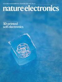
3D-printed soft electronicsHydrogel-based electronic devices can be fabricated using a stretchable silver–hydrogel ink and an embedded 3D-printing technology. The photograph on the cover shows a 3D-printed conductive structure embedded in a soft hydrogel matrix.
See Hui et al.
-
No. 11 November 2022
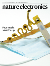
Face masks smarten upA conformable sensor interface that can be attached to the inside of a face mask can be used to monitor breathing patterns, skin temperature, verbal activity and the fit of the mask itself. The photograph on the cover shows the sensor interface, which incorporates a gecko-inspired thin adhesive layer that allows it to be repeatedly attached and detached from different commercial face masks.
See Kim et al. and News & Views by Adeel et al.
-
No. 10 October 2022
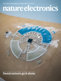
Sweat sensors go it aloneA wearable sweat sensor that integrates electrochemical sensors, a stretchable battery and an electrochromic display can directly display the concentration of various electrolytes or metabolites in sweat without any wired or wireless connection to external devices. The photograph on the cover shows the stretchable epidermal sweat-sensing patch, which can be worn during exercise and can provide real-time electrochemical data.
See Yin et al. and News & Views by Bandodkar
-
No. 9 September 2022
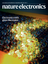
Electronics with glass-like statesElectronically controllable structural states in vanadium dioxide that exhibit features similar to glasses could be used to create a platform for high-performance data storage and processing. The computer-generated image on the cover highlights the nanoscopic conductive filaments that form in the vanadium dioxide and can store information.
See Nikoo et al.
-
No. 8 August 2022
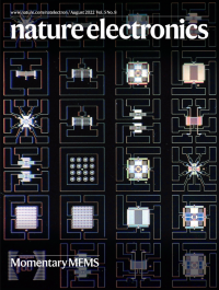
Momentary MEMSMicroelectromechanical systems (MEMS) that are based on water-soluble materials can resorb into the environment to eliminate waste, or into the body to avoid the need for surgical extraction, after a targeted lifetime. The photograph on the cover shows various ecoresorbable and bioresorbable MEMS devices supported within a single die.
See Yang et al.
-
No. 7 July 2022
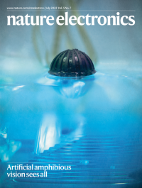
Artificial amphibious vision sees allAn amphibious artificial vision system with a panoramic field of view can be created by mimicking the functional and anatomical structure of the compound eyes of fiddler crabs. The photograph on the cover shows the artificial visual system, which integrates a microlens array with a flexible comb-shaped silicon photodiode array on a spherical structure.
See Lee et al.
-
No. 6 June 2022
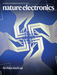
AI chips stack upStackable chips that use optoelectronic device arrays for chip-to-chip communication and neuromorphic cores based on memristor crossbar arrays for parallel data processing could be used to create energy-efficient sensor-computing systems for artificial intelligence (AI) applications. The optical microscopy image on the cover shows an AI processor chip, which can be combined with a range of different sensor and computing chips depending on the requirements of the application.
See Choi et al. and News & Views by Miao
-
No. 5 May 2022
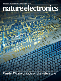
Van der Waals contacts on the wafer scaleHigh-quality van der Waals contacts between two-dimensional materials and three-dimensional metal electrodes can be formed on the wafer scale using a metal transfer printing technique in which electrodes are deposited on a graphene substrate, delaminated and then transferred onto two-dimensional semiconductors. The computer-generated image on the cover highlights the delamination of an array of metal electrodes from a graphene layer.
See Liu et al. and News & Views by Kwon
-
No. 4 April 2022
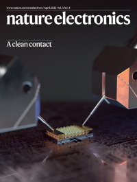
A clean contactWith the help of a metal deposition process that uses a selenium buffer layer, van der Waals contacts that are interaction- and defect-free can be formed between metals and two-dimensional semiconductors. The computer-generated image on the cover highlights the probing of p-type tungsten diselenide (WSe2) field-effect transistors with gold van der Waals contacts, which can be created with the technique.
See Kwon et al.
-
No. 3 March 2022
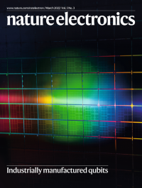
Industrially manufactured qubitsSilicon quantum dots and spin qubits can be fabricated in a 300-mm semiconductor manufacturing facility using all-optical lithography and fully industrial processing. The photograph on the cover shows a section of a 300-mm wafer that contains 82 unit cells (die) and more than 10,000 quantum dot arrays of various lengths.
See Zwerver et al.
-
No. 2 February 2022
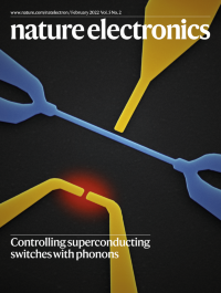
Controlling superconducting switches with phononsThe suppression of superconductivity in gated titanium nitride nanowires on silicon substrates can be linked to the relaxation of high-energy electrons and the emission of phonons. The cover shows a false-colour scanning electron microscopy image of a titanium nitride superconducting nanowire (blue) and side gates (yellow) on a silicon substrate. The generated phonons (red) travel through the substrate and efficiently switch the nanowire from a superconducting to a resistive state.
See Ritter et al.
-
No. 1 January 2022
The future of transportThe theme of our 2022 technology of the year is the future of transport, and we explore, in particular, key challenges in road transport.
See Editorial