
Abstract
Geometric diodes, which take advantage of geometric asymmetry to achieve current flow preference, are promising for THz current rectification. Previous studies relate geometric diodes’ rectification to quantum coherent or ballistic transport, which is fragile and critical of the high-quality transport system. Here we propose a different physical mechanism and demonstrate a robust current rectification originating from the asymmetric bias induced barrier lowering, which generally applies to common semiconductors in normal environments. Key factors to the diode’s rectification are carefully analyzed, and an intrinsic rectification ability at up to 1.1 THz is demonstrated.
Introduction
Diodes, the two-terminal electronic component that rectifies current in one direction, are among the simplest but most useful semiconductor devices1,2,3,4. p-n junction diodes and Schottky junction diodes are the most common solid-state rectifier diodes, which are widely used in power and signal processing circuits for AC-DC conversion, envelope detection, amplitude clipping, voltage regulation, etc5,6,7,8. p-n junction diodes have excellent rectification characteristics and high-voltage tolerance. However, as the minority carrier device, the p-n junction diode suffers from the minority charge storage, which hinders their high-frequency rectification performance9,10,11. Schottky junction diodes have gained attention as detectors, mixers, and frequency multipliers for high-frequency rectification because of their relatively high switching speeds. However, metal-semiconductor junctions are volatile and incapable of working at a high-voltage range12,13,14.
Besides p-n junction diodes and Schottky junction diodes, geometric diodes exhibit a geometric asymmetry related to rectification, which has been a long-pursued issue since the late 1990s15,16,17. The rectification of geometric diodes has been related to quantum coherent or ballistic transport, which is fragile and critical of the transport system. And their operation and high-frequency performance have been simulated with Monte Carlo simulations18. However, geometric diodes had been only experimentally demonstrated on high-mobility III–V semiconductor materials and graphene19,20,21,22,23,24. A recent paper has reported a silicon nanowire-based geometric diode, which enabled robust current rectification at room temperature24. The current rectification was attributed to a ratchet-like quasi-ballistic transport in diodes, which might be over-idealized for doped vapor-liquid-solid grown silicon nanowires at room temperature. (see Supplementary Note 1 and Supplementary Fig. 1 for details).
In this work, we have investigated the alternative origin of robust rectification in geometric diodes. We have demonstrated a robust current flow preference originated from an asymmetric bias-induced-barrier lowering (BIBL), while the ballistic transport or quantum coherent is not a necessity. We find that the current rectification is well reproducible using a basic electrostatic semiconductor physics model and shows good accordance with the experimental observations. We carefully analyze several vital factors to the geometric diode, such as the diode geometry, surface charging, passivation, and temperature. The geometric diode demonstrates an intrinsic rectification ability at up to 1.1 THz, showing their potential advantage in the THz range. This work provides a fundamental comprehension of geometric diodes, reveals their essential physical mechanisms, and extends their applicable range from specific high-mobility candidates to all general semiconductor materials.
Results and discussion
Asymmetric bias-induced barrier lowering
The simulative models are performed and more detailed information in the models of geometric diodes is provided in “Methods”. The geometric diode features an asymmetrical bottleneck and we set the geometric parameters and doping profile as shown in Fig. 1a. Our initial simulation did not show significant current rectification, as shown in the inset diagram of Fig. 1b. The absence of current rectification is in accordance with the finite-element simulation in the previous work24, where the quasi-ballistic model was concluded. However, we note that the surface states, which are well-known to exist at the surface of silicon, may also affect the current rectification of silicon nanowire geometric diodes. In previous works25,26, the surface state density (SSD) of silicon ranges from 1013 to 1011 cm−2. Therefore, we tried different SSD in the range of 1013 to 1011 cm−2 and found that the SSD of ~1012 cm−2 in the model can reproduce and perform good current rectification characteristics. As shown in Fig. 1b, we added the surface states (2.5 × 1012 cm−2, acceptor-like) to the model, and the I-V curve shows an evident current rectification ratio of 67, indicating a basic electrostatic semiconductor device model can well reproduce the rectification behavior in the geometric diode. The simulated band diagrams are shown in Fig. 1d, e and Supplementary Fig. 2. Apparently, a potential barrier exists along the axial direction of the diode with the barrier height varying with the applied voltage, as summarized in Fig. 1c. The unbiased barrier height is 471 meV, which can be lowered by the applied bias voltage asymmetrically: the forward bias lowers the barrier more significantly, with the barrier height decreasing to 48 meV at 1 V, while the reverse bias lowers the barrier less significantly, with the barrier height decreasing to 193 meV at −1 V. The potential barrier, which can be asymmetrically lowered by the bias, is determinative to the carrier flow preference in the geometric diode. More complicated settings considering the trapping/release process of surface charge are simulated27. And the I-V curve also shows an obvious rectification ratio with the potential barrier asymmetrically lowered by the bias (see Supplementary Fig. 3). The trapping and release of the surface charge do partly pin the Fermi level, but the Fermi level is still movable, resulting in the asymmetric BIBL as shown in Supplementary Fig. 4.

a Upper: geometric parameter definition, outer wire diameter (D), constriction diameter (d), angle (θ), and constriction angle (φ). Lower: device geometry and donor distribution. D = 100 nm, d = 10 nm, θ = 5.29°, φ = 46°. The background is set to vacuum. Scale bar: 100 nm. b Inset: initially simulated I-V curve of silicon nanowire diode without surface states. Main: simulated I-V curve with a surface state density of 2.5 × 1012 cm−2. c The barrier heights along the geometric diode axis with the various voltage. (d–f) The band diagrams with the applied bias voltage of −1 V (d), 0 V (e), 1 V (f). The dashed lines represent the quasi-Fermi level of electrons in nonthermal equilibrium.
Here we expound on the mechanism of the geometric diode’s robust rectification behavior. As shown in Fig. 2a, the terminated atomic lattices at the surface generate surface states28,29,30. These surface states can give rise to the Fermi level pinning, making the narrow bottleneck fully depleted (see Supplementary Fig. 5)31,32. The full depletion region forms a potential barrier, which blocks the majority carrier (electron for the n doped channel in this case) transporting from one side to the other. As shown in Fig. 2b–d, the potential barrier height can be lowered by the bias, which is akin to the well-known drain-induced-barrier lowering (DIBL) in short channel field-effect transistors33,34,35. Due to the asymmetric geometry and the intense fringe field at the kink, the bias-induced-barrier lowering (BIBL) is asymmetric (See Supplementary Fig. 6). Compared with the typical metal-insulator-semiconductor gate, the fringe field at the kink is impalpable but influential to the barrier lowering. For forward bias (see Supplementary Fig. 6a), the fringe electrical field, or self-gating field, orients to the channel, depletes the carriers, and lowers the barrier height more significantly, which is akin to applying a positive gate voltage to an MIS structure. In contrast, for reverse bias (see Supplementary Fig. 6b), the self-gating field orients from the channel, accumulate the carriers, and prevents the barrier height from lowering, which is akin to applying a negative gate voltage to an MIS structure. The asymmetric BIBL results in the current flow preference of the diode, according to the Boltzmann distribution. Ideally, we have
where I+ and I− are the forward and reverse current, respectively, k is the Boltzmann constant, T is temperature, Ф+, and Ф− are the potential barrier heights at the forward and reverse bias. Therefore, the rectification can be well explained based on fundamental semiconductor physical principles. Note that our analysis does not exclude the ballistic transport or quantum coherent induced rectification, though, as has been demonstrated in graphene and III–V component geometric diodes18,19,20,21,22,23,24. However, such rectification is frail and critical of a high-quality transport system18,19,20,21,22,23,24. The BIBL induced rectification is robust and applies to a wide range of semiconductors without critical environmental requirements.

a Surface states, Fermi level pinning, depletion, and self-gating field effect. These surface states resulting from the terminated atomic lattices at the surface can give rise to the Fermi level pinning, making the narrow bottleneck fully depleted, which forms a potential barrier. b–d The band profiles of the diode at the reverse (b), zero (c), and forward bias (d). The solid black circles represent the majority carriers, the arrows represent the direction of the carriers. The small red arrow and the red cross indicate that the carriers are difficult to transport from right to left at a reverse bias (b), and the large green arrow and the green cross indicate that the carriers can easily transport from left to right at forward bias (d).
The generality of the asymmetric BIBL mechanism
Now we discuss the generality of the BIBL mechanism in geometric induced rectification. Firstly, in principle, the BIBL is based on basic semiconductor physics, therefore it should apply to a wide range of semiconductor materials (See Supplementary Fig. 7). We simulated gallium arsenide and germanium nanowire geometric diodes, as shown in Supplementary Fig. 7a, b. The I-V curves show an evident current rectification, indicating the BIBL mechanism is also applicable to the nanowire geometric diodes in other material systems except for silicon. Secondly, the self-gating effect applies to various asymmetric geometries. In a previous study, lateral gates short circuit to one terminal were elaborately added to achieve rectification36. Here we reveal that aiming to the asymmetric barrier lowering, and the evolutive geometries such as asymmetric kink can also generate obvious rectification, which simplifies the fabrication process, and more importantly for high-frequency devices, significantly reduces the parasitic capacitance (See Supplementary Fig. 8), as shown in Supplementary Fig. 7c and Fig. 8. Thirdly, the concept of the geometric diode can also be extended, which, for example, leads to a “doping diode”, as shown in Supplementary Fig. 7d. The device has symmetric geometry but an asymmetric doping profile, still, the asymmetric doping also generates a rectification ratio of up to 70. Lastly, although the above has discussed the n-type component geometric diode, the principle apparently applies to the analogous p-type component, which is not repetitiously discussed in this paper.
Key factors determining the geometric diode’s rectification
Based on the above comprehension, we have investigated several key factors determining the geometric diode’s rectification behavior:
-
(1)
Surface states: In the above discussion, surface states are necessary to deplete the doped channel and generate a potential barrier at the bottleneck. As shown in Fig. 3a, our simulation results show that for the doped nanowire geometric device, with increasing surface state density, the current rectification increases, reaching 7000 with a surface state density of 3.5 × 1012 cm−2 at room temperature (φ = 46°, θ = 5.29°, D = 100 nm, d = 10 nm). However, it should be noted that if the bottleneck of the nanowire is undoped, a potential barrier intrinsically exists, and therefore, the surface states are not necessary. The rectification ratio of a hypothetic surface state free geometric diode (which, it is realistically impossible to achieve for Si, the typical non-van der Waals devices) reaches 7 × 10⁵, as shown in Fig. 3b and Supplementary Fig. 10.
Fig. 3: Key factors in geometric diodes. 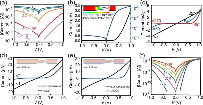
a Log scale I-V curves of five geometric diodes with the surface states of 0, 1 × 10¹², 2 × 10¹², 3 × 10¹², 3.5 × 1012 cm−2 at room temperature. The current decreases, and the rectification ratio increase with higher surface state density. b The I-V curve of geometric diodes with an undoped constrictive bottleneck. c The I-V curves simulated from three separate geometric diodes with φ of 25°, 64°, and 65°, respectively. The surface charge density was set at 1.3 × 1012 cm−2. d, e The I-V curves from the geometric diode wrapped with 10 nm SiO2 (d) and 10 nm Al2O3 (e), respectively. The charged surface state density was set at 4 × 1011 cm−2. f Log scale I-V curves of a geometric diode device at temperatures of 77 K (blue), 125 K (purple), 175 K (green), 250 K (yellow), and 350 K (red).
-
(2)
Geometry: As shown in Fig. 3c and Supplementary Fig. 11, we have simulated geometric diodes with various φ of 25°, 45°, 64°, 64.5°, and 65° (doped, doping profile is the same with Fig. 1a). An increased φ provides a more intense field-effect at the kink, resulting in the asymmetric BIBL. We observe a sudden increase of rectification ratio at φ > 64°, which is in good accordance with the experimental observation24.
-
(3)
Passivation: In the above simulation, the geometric diode was placed in the vacuum, where the self-gating field effect is relatively weak. The self-gating field effect and asymmetric BIBL can be further strengthened by the dielectric coating. In order to verify the effect of passivation, Fig. 3d, e shows the I-V curves with and without the surface passivation layer of 10 nm SiO2 and 10 nm Al2O3, respectively. The surface state density is set as low as 4 × 1011 cm−2. For the bare Si nanowire geometric diode, such low surface state density cannot cause distinct current rectification (black line). For the passivated, we observe the apparent current rectification ratio of 9 (SiO2) and 28 (Al2O3), respectively. Therefore, surface dielectric passivation can significantly enhance asymmetric BIBL and the current rectification of the geometric diode. The passivation enhanced current rectification and also evidenced the self-gating field-effect illustrated in Supplementary Fig. 6.
-
(4)
Temperature: according to Eq. (1), the rectification ratio monotonically decreases with temperature. Figure 3f shows the simulated temperature-dependent I-V curves of the geometric diode, indicating the rectification ratio dramatically increases with decreased temperature. Note that both the reverse and forward current were diminished as the temperature decreased, which is in accordance with the experimental observation. Because fewer carriers can transport over the barrier at a lower temperature. Besides the statistical thermodynamics, the decrease in current could also be caused by the increase in surface charge trapped at low temperatures, which was observed in the previous study36.

High-frequency of geometric diodes
Diodes working at the THz range are essential for the high throughput signal processing and communication technology. Due to the absence of minority carrier storage, geometric diodes are promising to achieve higher frequency current rectification over p-n junction diodes and even Schottky junction diodes (See Supplementary Fig. 12). Here we present the high-frequency response of the geometric diode. The DC I-V curve of the geometric diode is shown in Fig. 4a, with a DC rectification ratio (±1 V) of 10. Such rectification maintains at an AC stimulation with frequency up to around 100 GHz, as shown in Fig. 4b and Fig. 4c, d. The rectification ratio drops significantly at a higher frequency, still, a rectification ratio of 2 is obtained at 1.1 THz, indicating that the diode can provide effective current rectification at the THz range, as shown in Fig. 4e–k. The geometric diode further loses its rectification ability at a higher frequency, and the rectification ratio decreases down to 1.1 at 2 THz, as shown in Fig. 4l–n. Therefore, the geometric diode has significant advantages at the THz range, showing great potential in ultra-fast signal processing circuits, 6 G communications, and THz radar and electromagnetic wave energy harvesting.

a The static I-V of silicon nanowires geometric diode showing a rectification ratio of 10. b The rectification ratio of the geometric diode with frequency varying from 40 GHz to 2 THz. The current response of the geometric diode with a rectification ratio of c 9.5 at 40 GHz, d 9.4 at 100 GHz, e 8.5 at 200 GHz, f 6.9 at 300 GHz, g 4.2 at 500 GHz, h 2.7 at 800 GHz, i 2.4 at 900 GHz, j 2.2 at 1 THz, k 2.0 at 1.1 THz, l 1.8 at 1.2 THz, m 1.5 at 1500 GHz, and n 1.2 at 2 THz, respectively.
Conclusion
In summary, this work proposes a robust rectification mechanism in the geometric diode. The robust rectification originates from the asymmetric bias-induced barrier lowering on the basis of fundamental physical principles of semiconductor devices. Therefore, such robust rectification applies not critically to the high-mobility candidates but generally to all semiconductors. Key factors to the geometric diode such as surface states, geometry, surface passivation, and temperature are carefully analyzed, and the intrinsic rectification ability in the THz range is demonstrated. This work provides a fundamental comprehension of the geometric diode, which shows excellent potential in THz circuits.
Methods
Simulation details
-
1.
Electrostatic model
-
2.
Monte Carlo model
In the Monte Carlo model, the electrostatic parameter is set the same as that in the Table 1 model. Only major carriers transportation (i.e., an electron in this work) were simulated, the relaxation time of electron was set 0.3 ps and the number of iterations was set 50. The electron specular reflection was set from 60 to 100%, none of which show obvious current rectification. Supplementary Fig. 1 shows the simulative results with the specular reflection of 100%, which were expected to exhibit the largest rectification ratio.
Data availability
The data that support the findings of this study are available from the corresponding authors upon reasonable request.
Code availability
The codes used to generate the data presented in the manuscript are available from the corresponding author on reasonable request.
References
Wunsch, D. C. & Bell, R. R. Determination of threshold failure levels of semiconductor diodes and transistors due to pulse voltages. IEEE Trans. Nucl. Sci. 15, 244–259 (1968).
Burroughes, J. H., Jones, C. A. & Friend, R. H. New semiconductor device physics in polymer diodes and transistors. Nature 335, 137–141 (1988).
Seeds, A. J. & Salles, A. A. A. D. Optical control of microwave semiconductor devices. IEEE Trans. Microw. Theory Tech. 38, 577–585 (1990).
Lauritzen, P. O. & Ma, C. L. A simple diode model with reverse recovery. IEEE Trans. Power Electron. 6, 188–191 (1991).
Lyakas, M., Zaharia, R. & Eizenberg, M. Analysis of nonideal Schottky and p‐n junction diodes—Extraction of parameters from I–V plots. J. Appl. Phys. 78, 5481–5489 (1995).
Shah, J. M., Li, Y. L., Gessmann, T. & Schubert, E. F. Experimental analysis and theoretical model for anomalously high ideality factors (n ≫ 2.0) in AlGaN/GaN pn junction diodes. J. Appl. Phys. 94, 2627–2630 (2003).
Deb, P. et al. GaN Nanorod Schottky and p−n junction diodes. Nano Lett. 6, 2893–2898 (2006).
Lee, J. U., Gipp, P. P. & Heller, C. M. Carbon nanotube p-n junction diodes. Appl. Phys. Lett. 85, 145–147 (2004).
Pearson, G. L. & Sawyer, B. Silicon pn junction alloy diodes. Proc. Inst. Electr. Eng. 40, 1348–1351 (1952).
Liou, J. J. & Lindholm, F. A. Capacitance of semiconductor p-n junction space-charge layers: an overview. Proc. IEEE Inst. Electr. Electron Eng. 76, 1406–1422 (1988).
Rahimo, M. T. & Shammas, N. Y. A. Freewheeling diode reverse-recovery failure modes in IGBT applications. IEEE Trans. Ind. Appl. 37, 661–670 (2001).
Manohara, H. M., Wong, E. W., Schlecht, E., Hunt, B. D. & Siegel, P. H. Carbon nanotube Schottky diodes using Ti-Schottky and Pt-Ohmic contacts for high frequency applications. Nano Lett. 5, 1469–1474 (2005).
Tonouchi, M. Cutting-edge terahertz technology. Nat. Photon. 1, 97–105 (2007).
Valletta, A. et al. Threshold voltage in short channel polycrystalline silicon thin film transistors: Influence of drain induced barrier lowering and floating body effects. J. Appl. Phys. 107, 074505 (2010).
Linke, H. et al. A quantum dot ratchet: experiment and theory. Europhys. Lett. 44, 341 (1998).
Song, A. M. et al. Nonlinear electron transport in an asymmetric microjunction: a ballistic rectifier. Phys. Rev. Lett. 80, 3831 (1998).
Linke, H. et al. Experimental tunneling ratchets. Science 286, 2314–2317 (1999).
Mateos, J. et al. Ballistic nanodevices for terahertz data processing: Monte Carlo simulations. Nanotechnology 14, 117 (2003).
Sassine, S. et al. Experimental investigation of the ratchet effect in a two-dimensional electron system with broken spatial inversion symmetry. Phys. Rev. B 78, 045431 (2008).
Dragoman, M., Muller, A. A., Dragoman, D., Coccetti, F. & Plana, A. R. Terahertz antenna based on graphene. J. Appl. Phys. 107, 104313 (2010).
Tongay, S. et al. Rectification at graphene-semiconductor interfaces: zero-gap semiconductor-based diodes. Phys. Rev. X 2, 011002 (2012).
Aldrigo, M., Dragoman, M., Costanzo, A. & Dragoman, D. Graphene as a high impedance surface for ultra-wideband electromagnetic waves. J. Appl. Phys. 114, 184308 (2013).
Auton, G. et al. Graphene ballistic nano-rectifier with very high responsivity. Nat. Commun. 7, 1–6 (2016).
Custer, J. P. et al. Ratcheting quasi-ballistic electrons in silicon geometric diodes at room temperature. Science 368, 177–180 (2020).
Terlinden, N. M., Dingemans, G., Vandalon, V., Bosch, R. H. E. C. & Kessels, W. M. M. Influence of the SiO2 interlayer thickness on the density and polarity of charges in Si/SiO2/Al2O3 stacks as studied by optical second-harmonic generation. J. Appl. Phys. 115, 033708 (2014).
Schmidt, V., Senz, S. & Gosele, U. Influence of the Si/SiO2 interface on the charge carrier density of Si nanowires. Appl. Phys. A 86, 187–191 (2007).
Iñiguez-De-La-Torre, I. et al. Influence of the surface charge on the operation of ballistic T-branch junctions: a self-consistent model for Monte Carlo simulations. Semiconductor Sci. Technol. 22, 663 (2007).
Zhang, Z. & Yates, J. T. Jr. Band bending in semiconductors: chemical and physical consequences at surfaces and interfaces. Chem. Rev. 112, 5520–5551 (2012).
Dhara, S., Mele, E. J. & Agarwal, R. Voltage-tunable circular photogalvanic effect in silicon nanowires. Science 349, 726–729 (2015).
Boles, M. A., Ling, D., Hyeon, T. & Talapin, D. V. The surface science of nanocrystals. Nat. Mater. 15, 141–153 (2016).
Shen, Y., Hosseini, A. R., Wong, M. H. & Malliaras, G. G. How to make ohmic contacts to organic semiconductors. Chemphyschem 5, 16–25 (2004).
Sotthewes, K. et al. Universal Fermi-level pinning in transition-metal dichalcogenides. J. Phys. Chem. C. 123, 5411–5420 (2019).
Chamberlain, S. G. & Ramanan, S. Drain-induced barrier-lowering analysis in VSLI MOSFET devices using two-dimensional numerical simulations. IEEE Trans. Electron Devices 33, 1745–1753 (1986).
Chaudhry, A. & Kumar, M. J. Controlling short-channel effects in deep-submicron SOI MOSFETs for improved reliability: a review. IEEE Trans. Device Mater. Rel. 4, 99–109 (2004).
Tsuchiya, T., Sato, Y. & Tomizawa, M. Three mechanisms determining short-channel effects in fully-depleted SOI MOSFETs. IEEE Trans. Electron Devices 45, 1116–1121 (1998).
Pérez-Martín, E. et al. Trap-related frequency dispersion of zero-bias microwave responsivity at low temperature in GaN-based self-switching diodes. Nanotechnology 31, 405204 (2020).
Acknowledgements
We thank Prof. James F. Cahoon, the author of the previous work24, for the response to our queries. We also thank the Analysis & Testing Center, Beijing Institute of Technology. This work is supported by the National Natural Science Foundation of China grant 11804024.
Author information
Authors and Affiliations
Contributions
Y.G. supervised and managed the work. M.B., Y.Z., S.X., and T.T. performed the simulation and analyzed the data. M.B. wrote the manuscript. All authors discussed the results and contributed to the manuscript.
Corresponding author
Ethics declarations
Competing interests
The authors declare no competing interests.
Additional information
Peer review information Communications Physics thanks Javier Mateos, Alessandro Pitanti and the other, anonymous, reviewer(s) for their contribution to the peer review of this work. Peer reviewer reports are available.
Publisher’s note Springer Nature remains neutral with regard to jurisdictional claims in published maps and institutional affiliations.
Supplementary information
Rights and permissions
Open Access This article is licensed under a Creative Commons Attribution 4.0 International License, which permits use, sharing, adaptation, distribution and reproduction in any medium or format, as long as you give appropriate credit to the original author(s) and the source, provide a link to the Creative Commons license, and indicate if changes were made. The images or other third party material in this article are included in the article’s Creative Commons license, unless indicated otherwise in a credit line to the material. If material is not included in the article’s Creative Commons license and your intended use is not permitted by statutory regulation or exceeds the permitted use, you will need to obtain permission directly from the copyright holder. To view a copy of this license, visit http://creativecommons.org/licenses/by/4.0/.
About this article

Cite this article
Bai, M., Zhao, Y., Xu, S. et al. Asymmetric bias-induced barrier lowering as an alternative origin of current rectification in geometric diodes. Commun Phys 4, 236 (2021). https://doi.org/10.1038/s42005-021-00735-9
Received:
Accepted:
Published:
DOI: https://doi.org/10.1038/s42005-021-00735-9
This article is cited by
-
Ultrasensitive rapid cytokine sensors based on asymmetric geometry two-dimensional MoS2 diodes
Nature Communications (2022)
Comments
By submitting a comment you agree to abide by our Terms and Community Guidelines. If you find something abusive or that does not comply with our terms or guidelines please flag it as inappropriate.
