Abstract
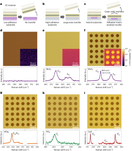
Pristine van der Waals (vdW) heterostructures formed between two-dimensional (2D) and other materials can be used to create optical and electronic devices. However, the weak vdW forces alone do not allow direct physical stacking of arbitrary layers. As a result, vdW heterostructure fabrication typically requires solvents, sacrificial layers or high temperatures, which can introduce damage and contaminants. Here, we show that adhesive matrix transfer can eliminate these limitations and can provide vdW integration beyond the limits of vdW forces. In the approach, a hybrid high- and low-adhesion surface is used to decouple the forces driving the transfer from the vdW forces defining the heterostructure of interest. We show that the technique can be used to achieve direct vdW integration of diverse 2D materials (MoS2, WSe2, PtS2 and GaS) with dielectrics (SiO2 and Al2O3), which is conventionally forbidden but critical for active devices and scalable, aligned heterostructure formation. The approach also allows single-step 2D material-to-device integration, which we illustrate by fabricating arrays of monolayer MoS2 transistors. As any exposure to solvents or polymers is avoided, the interfaces and surfaces remain pristine. Thus, intrinsic 2D material properties can be probed without the influence of processing steps. The materials can be further engineered through surface treatments and used to fabricate unconventional device form factors.
This is a preview of subscription content, access via your institution
Access options
Access Nature and 54 other Nature Portfolio journals
Get Nature+, our best-value online-access subscription
$29.99 / 30 days
cancel any time
Subscribe to this journal
Receive 12 digital issues and online access to articles
$119.00 per year
only $9.92 per issue
Buy this article
- Purchase on Springer Link
- Instant access to full article PDF
Prices may be subject to local taxes which are calculated during checkout


Data availability
The data that support the plots within this paper and other findings of this study are available from the corresponding authors on reasonable request.
Code availability
The source code for processing the data is available from the corresponding author upon request.
References
Bhimanapati, G. R. et al. Recent advances in two-dimensional materials beyond graphene. ACS Nano 9, 11509–11539 (2015).
Jariwala, D., Marks, T. J. & Hersam, M. C. Mixed-dimensional van der Waals heterostructures. Nat. Mater. 16, 170–181 (2017).
Liu, Y., Huang, Y. & Duan, X. Van der Waals integration before and beyond two-dimensional materials. Nature 567, 323–333 (2019).
Israelachvili, J. Intermolecular and Surface Forces (Academic Press, 2011).
Schranghamer, T. F., Sharma, M., Singh, R. & Das, S. Review and comparison of layer transfer methods for two-dimensional materials for emerging applications. Chem. Soc. Rev. 50, 11032–11054 (2021).
Shim, J. et al. Controlled crack propagation for atomic precision handling of wafer-scale two-dimensional materials. Science 362, 665–670 (2018).
Liang, X. et al. Toward clean and crackless transfer of graphene. ACS Nano 5, 9144–9153 (2011).
Lin, Y.-C. et al. Graphene annealing: how clean can it be? Nano Lett. 12, 414–419 (2012).
Pirkle, A. et al. The effect of chemical residues on the physical and electrical properties of chemical vapor deposited graphene transferred to SiO2. Appl. Phys. Lett. 99, 122108 (2011).
Islam, A., Lee, J. & Feng, P. X. L. All-dry transferred single- and few-layer MoS2 field effect transistor with enhanced performance by thermal annealing. J. Appl. Phys. 123, 025701 (2018).
Castellanos-Gomez, A. et al. Deterministic transfer of two-dimensional materials by all-dry viscoelastic stamping. 2D Mater. 1, 011002 (2014).
Caldwell, J. D. et al. Technique for the dry transfer of epitaxial graphene onto arbitrary substrates. ACS Nano 4, 1108–1114 (2010).
Pizzocchero, F. et al. The hot pick-up technique for batch assembly of van der Waals heterostructures. Nat. Commun. 7, 11894 (2016).
Watson, A. J., Lu, W., Guimarães, M. H. D. & Stöhr, M. Transfer of large-scale two-dimensional semiconductors: challenges and developments. 2D Mater. 8, 032001 (2021).
Liu, Y. et al. Approaching the Schottky–Mott limit in van der Waals metal–semiconductor junctions. Nature 557, 696–700 (2018).
Jung, Y. et al. Transferred via contacts as a platform for ideal two-dimensional transistors. Nat. Electron. 2, 187–194 (2019).
Liu, L. et al. Transferred van der Waals metal electrodes for sub-1-nm MoS2 vertical transistors. Nat. Electron. 4, 342–347 (2021).
Liu, G. et al. Graphene-assisted metal transfer printing for wafer-scale integration of metal electrodes and two-dimensional materials. Nat. Electron. 5, 275–280 (2022).
Poddar, P. K. et al. Resist-free lithography for monolayer transition metal dichalcogenides. Nano Lett. 22, 726–732 (2022).
Velický, M. et al. Strain and charge doping fingerprints of the strong interaction between monolayer MoS2 and gold. J. Phys. Chem. Lett. 11, 6112–6118 (2020).
Liu, F. et al. Disassembling 2D van der Waals crystals into macroscopic monolayers and reassembling into artificial lattices. Science 367, 903–906 (2020).
Heyl, M. et al. Thermally activated gold‐mediated transition metal dichalcogenide exfoliation and a unique gold‐mediated transfer. Phys. Status Solidi Rapid Res. Lett. 14, 2000408 (2020).
Li, Z. et al. Dry exfoliation of large-area 2D monolayer and heterostructure arrays. ACS Nano 15, 13839–13846 (2021).
Lee, C. et al. Anomalous lattice vibrations of single- and few-layer MoS2. ACS Nano 4, 2695–2700 (2010).
Splendiani, A. et al. Emerging photoluminescence in monolayer MoS2. Nano Lett. 10, 1271–1275 (2010).
Zhao, W. et al. Lattice dynamics in mono- and few-layer sheets of WS2 and WSe2. Nanoscale 5, 9677–9683 (2013).
Zhao, Y. et al. Extraordinarily strong interlayer interaction in 2D layered PtS2. Adv. Mater. 28, 2399–2407 (2016).
Gutiérrez, Y., Giangregorio, M. M., Dicorato, S., Palumbo, F. & Losurdo, M. Exploring the thickness-dependence of the properties of layered gallium sulfide. Front. Chem. 9, 781467 (2021).
Vogel, N., Zieleniecki, J. & Köper, I. As flat as it gets: ultrasmooth surfaces from template-stripping procedures. Nanoscale 4, 3820–3832 (2012).
Velický, M. et al. Mechanism of gold-assisted exfoliation of centimeter-sized transition-metal dichalcogenide monolayers. ACS Nano 12, 10463–10472 (2018).
Bordag, M., Mohideen, U. & Mostepanenko, V. M. New developments in the Casimir effect. Phys. Rep. 353, 1–205 (2001).
Huang, Y. et al. Universal mechanical exfoliation of large-area 2D crystals. Nat. Commun. 11, 2453 (2020).
Lifshitz, E. M. & Hamermesh, M. The theory of molecular attractive forces between solids. Perspect. Theor. Phys. 26, 329–349 (1992).
Drosdoff, D. & Woods, L. M. Casimir forces and graphene sheets. Phys. Rev. B Condens. Matter Mater. Phys. 82, 155459 (2010).
Khurgin, J. B. Expanding the photonic palette: exploring high index materials. ACS Photonics 9, 743–751 (2022).
Wei, Z. et al. Scratching lithography for wafer-scale MoS2 monolayers. 2D Mater. 7, 045028 (2020).
Liu, X., Howell, S. T., Conde‐Rubio, A., Boero, G. & Brugger, J. Thermomechanical nanocutting of 2D materials. Adv. Mater. 32, 2001232 (2020).
Blake, P. et al. Making graphene visible. Appl. Phys. Lett. 91, 063124 (2007).
Ferrari, A. C. et al. Raman spectrum of graphene and graphene layers. Phys. Rev. Lett. 97, 187401 (2006).
Neumann, C. et al. Raman spectroscopy as probe of nanometre-scale strain variations in graphene. Nat. Commun. 6, 8429 (2015).
Ding, F. et al. Stretchable graphene: a close look at fundamental parameters through biaxial straining. Nano Lett. 10, 3453–3458 (2010).
Lee, J. E., Ahn, G., Shim, J., Lee, Y. S. & Ryu, S. Optical separation of mechanical strain from charge doping in graphene. Nat. Commun. 3, 1024 (2012).
Bendiab, N. et al. Unravelling external perturbation effects on the optical phonon response of graphene. J. Raman Spectrosc. 49, 130–145 (2018).
Aitken, Z. H. & Huang, R. Effects of mismatch strain and substrate surface corrugation on morphology of supported monolayer graphene. J. Appl. Phys. 107, 123531 (2010).
Liu, F., Navaraj, W. T., Yogeswaran, N., Gregory, D. H. & Dahiya, R. Van der Waals contact engineering of graphene field-effect transistors for large-area flexible electronics. ACS Nano 13, 3257–3268 (2019).
Fan, X. et al. Graphene ribbons with suspended masses as transducers in ultra-small nanoelectromechanical accelerometers. Nat. Electron. 2, 394–404 (2019).
Fan, X. et al. Suspended graphene membranes with attached silicon proof masses as piezoresistive nanoelectromechanical systems accelerometers. Nano Lett. 19, 6788–6799 (2019).
Ruiz-Vargas, C. S. et al. Softened elastic response and unzipping in chemical vapor deposition graphene membranes. Nano Lett. 11, 2259–2263 (2011).
Cartamil-Bueno, S. J. et al. Very large scale characterization of graphene mechanical devices using a colorimetry technique. Nanoscale 9, 7559–7564 (2017).
Liu, X., Yuan, Y., Qu, D. & Sun, J. Ambipolar MoS2 field‐effect transistor by spatially controlled chemical doping. Phys. Status Solidi Rapid Res. Lett. 13, 1900208 (2019).
Wang, Y. et al. P-type electrical contacts for 2D transition-metal dichalcogenides. Nature 610, 61–66 (2022).
Pu, J. et al. Highly flexible MoS2 thin-film transistors with ion gel dielectrics. Nano Lett. 12, 4013–4017 (2012).
Cheng, R. et al. Few-layer molybdenum disulfide transistors and circuits for high-speed flexible electronics. Nat. Commun. 5, 5143 (2014).
Daus, A. et al. High-performance flexible nanoscale transistors based on transition metal dichalcogenides. Nat. Electron. 4, 495–501 (2021).
Vogel, N. et al. Laterally patterned ultraflat surfaces. Small 5, 821–825 (2009).
Leplan, H., Geenen, B., Robic, J. Y. & Pauleau, Y. Residual stresses in evaporated silicon dioxide thin films: correlation with deposition parameters and aging behavior. J. Appl. Phys. 78, 962–968 (1995).
Gruber, W. et al. Strain relaxation and vacancy creation in thin platinum films. Phys. Rev. Lett. 107, 265501 (2011).
Soled, S., Wold, A. & Gorochov, O. Crystal growth and characterization of several platinum sulfoselenides. Mater. Res. Bull. 11, 927–932 (1976).
Lieth, R. M. A., Van Der Heijden, C. W. M. & Van Kessel, J. W. M. Preparation, purity and electrical conductivity of gallium sulphide single crystals. J. Cryst. Growth 5, 251–258 (1969).
Li, X. et al. Transfer of large-area graphene films for high-performance transparent conductive electrodes. Nano Lett. 9, 4359–4363 (2009).
Park, H. et al. Optimized poly(methyl methacrylate)-mediated graphene-transfer process for fabrication of high-quality graphene layer. Nanotechnology 29, 415303 (2018).
Her, M., Beams, R. & Novotny, L. Graphene transfer with reduced residue. Phys. Lett. A 377, 1455–1458 (2013).
Ling, X. et al. Role of the seeding promoter in MoS2 growth by chemical vapor deposition. Nano Lett. 14, 464–472 (2014).
Ylivaara, O. M. E. et al. Aluminum oxide from trimethylaluminum and water by atomic layer deposition: the temperature dependence of residual stress, elastic modulus, hardness and adhesion. Thin Solid Films 552, 124–135 (2014).
Li, N. et al. Large-scale flexible and transparent electronics based on monolayer molybdenum disulfide field-effect transistors. Nat. Electron. 3, 711–717 (2020).
Acknowledgements
This work was supported by the National Science Foundation (NSF; Award No. CMMI-2135846) and the NSF Center for Energy Efficient Electronics Science (Award No. ECCS-0939514). P.F.S., P.J.-P. and S.O.S. acknowledge support from the NSF Graduate Research Fellowship Program (Grant No. 1745302). The work by H.G. and X.L. was supported by the US Department of Energy, Office of Science, Basic Energy Sciences (Award No. DE-SC0021064). The work by X.L., Q.T. and H.K. was supported by the NSF (Award No. CHE-1945364). H.G. acknowledges support from a BUnano Cross-Disciplinary Fellowship at Boston University. A.-Y.L. and J.K. acknowledge support from the US Army Research Office through the Institute for Soldier Nanotechnologies at the Massachusetts Institute of Technology (MIT; Cooperative Agreement No. W911NF-18-2-0048). The fabrication and characterization procedures in this work were in part carried out using the MIT.nano shared facilities. We thank the research staff of MIT.nano, in particular K. Broderick, W. Hess, J. Scholvin, D. Terry and D. Ward, for their support of this work. P.F.S. would further like to thank J. Zhu for electrical measurement advice, N. Romeo for help with mechanical modelling and M. Saravanapavanantham for characterization support. The TEM sample preparation and imaging were performed at the Harvard University Center for Nanoscale Systems with the help of S. Kraemer and J. Gardener. The Center for Nanoscale Systems is a member of the National Nanotechnology Coordinated Infrastructure Network, which is supported by the NSF (ECCS Award No. 1541959).
Author information
Authors and Affiliations
Contributions
P.F.S. and F.N. conceived the project, designed the experiments and wrote the manuscript. P.F.S. performed the experiments and analysed the results. P.F.S., P.-J.P., W.Z. and F.N. developed the template-stripping process. W.Z. assisted with the photoluminescence measurements. P.F.S., M.T. and F.N. developed the MoS2 transfer process. S.O.S. assisted with TEM sample preparation and imaging. H.G. and X.L. grew the CVD MoS2. S.-Y.T., Y.-L.C., C.-N.K. and C.S.L. grew the PtS2. Q.T. and X.L. grew the GaS. P.F.S., H.K., A.-Y.L., J.K., X.L. and F.N. developed the graphene transfer process. F.N. supervised the project. All authors contributed to finalizing the manuscript.
Corresponding author
Ethics declarations
Competing interests
The authors declare no competing interests.
Peer review
Peer review information
Nature Electronics thanks Mengjian Zhu and the other, anonymous, reviewer(s) for their contribution to the peer review of this work.
Additional information
Publisher’s note Springer Nature remains neutral with regard to jurisdictional claims in published maps and institutional affiliations.
Supplementary information
Supplementary Information
Supplementary Figs. 1–15, Tables 1–5 and Notes 1–6.
Rights and permissions
Springer Nature or its licensor (e.g. a society or other partner) holds exclusive rights to this article under a publishing agreement with the author(s) or other rightsholder(s); author self-archiving of the accepted manuscript version of this article is solely governed by the terms of such publishing agreement and applicable law.
About this article
Cite this article
Satterthwaite, P.F., Zhu, W., Jastrzebska-Perfect, P. et al. Van der Waals device integration beyond the limits of van der Waals forces using adhesive matrix transfer. Nat Electron 7, 17–28 (2024). https://doi.org/10.1038/s41928-023-01079-8
Received:
Accepted:
Published:
Issue Date:
DOI: https://doi.org/10.1038/s41928-023-01079-8
This article is cited by
-
Breaking the limitation of van der Waals integration
Nature Reviews Materials (2024)


