
Abstract
The control of elastic and inelastic electron tunnelling relies on materials with well-defined interfaces. Two-dimensional van der Waals materials are an excellent platform for such studies. Signatures of acoustic phonons and defect states have been observed in current-to-voltage measurements. These features can be explained by direct electron–phonon or electron–defect interactions. Here we use a tunnelling process that involves excitons in transition metal dichalcogenides (TMDs). We study tunnel junctions consisting of graphene and gold electrodes separated by hexagonal boron nitride with an adjacent TMD monolayer and observe prominent resonant features in current-to-voltage measurements appearing at bias voltages that correspond to TMD exciton energies. By placing the TMD outside of the tunnelling pathway, we demonstrate that this tunnelling process does not require any charge injection into the TMD. The appearance of such optical modes in electrical transport introduces additional functionality towards van der Waals material–based optoelectronic devices.
Main
The isolation of two-dimensional (2D) crystals combined with advances in fabrication techniques has enabled the realization of new types of materials, known as van der Waals heterostructures, in which different atomic layers are assembled together in a desired sequence1. Tailored heterostructures comprising graphene, hexagonal boron nitride (hBN), TMDs and other 2D materials are currently designed to display properties that are absent in the individual constituents, thus providing a platform for fundamental studies2,3,4,5,6,7 and novel device applications8,9,10. In this respect, tunnel junctions with different material combinations form an interesting system for investigating electron tunnelling processes. Previous experiments have shown phonon-assisted resonant electron tunnelling in metal–insulator junctions11, in conventional semiconductor heterostructures12 and in graphene-based systems13,14,15,16. Similarly, exciton-assisted resonant tunnelling has been observed in conventional semiconductor quantum wells17,18. Plasmon-assisted resonant tunnelling has been investigated in metallic quantum well structures hosting silver nanorods19 and graphene-based structures20. Furthermore, evidence for defect-assisted resonant tunnelling has been observed in hBN-based junctions21.
Here we demonstrate exciton-assisted resonant electron tunnelling in van der Waals tunnel junctions. Our electron transport measurements reveal distinct resonant peaks that coincide in energy with TMD excitons. We investigate the current-to-voltage (I−V) characteristics of TMD/graphene/hBN/Au tunnel junctions and compare them with TMD-free reference structures. Resonances observed in differential conductance (dI/dV) measurements agree with TMD exciton energies despite the fact that the TMD is placed outside the electron tunnelling pathway. These resonances can be explained by a one-step process involving indirect excitons and a two-step process involving both phonons and direct excitons. Both of these processes conserve energy and in-plane momentum. Owing to the large exciton binding energies of TMD monolayers22,23, such as WS2, MoS2, WSe2 and MoSe2, the resonant features can be observed at room temperature. While exciton–phonon interactions in TMDs have been investigated by optical methods24,25,26,27, our study observes this interaction directly in electronic transport measurements, shedding light on the ways excitons are involved in the conservation of momentum during tunnelling. Beyond its fundamental interest, our work establishes a platform for the investigation of the physical processes involved in the electrical generation of excitons in TMDs.
Our reference device is illustrated in Fig. 1a, where the graphene and Au electrodes are separated by a 3–4 nm layer of insulating hBN. Applying a bias voltage between the two electrodes generates a tunnel current through the hBN barrier. The band diagram is depicted in Fig. 1b for a positive bias voltage Vb. The inelastic electron tunnelling process, indicated by the kinked arrow, can be mediated by different modes of the structure, including phonons, defects, photons and surface plasmons28,29,30,31. The measured I−V curve of such a device is plotted in red in Fig. 1c, which features a nearly exponential dependence on Vb for both polarities, in agreement with previous reports32,33. To gain further insight, we evaluate the differential conductance dI/dV, shown in blue in Fig. 1c. This plot reveals an asymmetry in bias voltage (that is, the differential conductance increases more rapidly for negative Vb). This can be understood by the abrupt increase of the electronic density of states in Au for negative bias voltages (Supplementary Fig. 9). In addition, some minute features can be observed near the zero bias region, as shown in the inset of Fig. 1c. The minimum appearing around Vb = 0 V is claimed to be a signature of inelastic electron tunnelling assisted by graphene phonons14. The latter mediate the in-plane momentum mismatch between the electronic states in Au and graphene13,14,15,30.
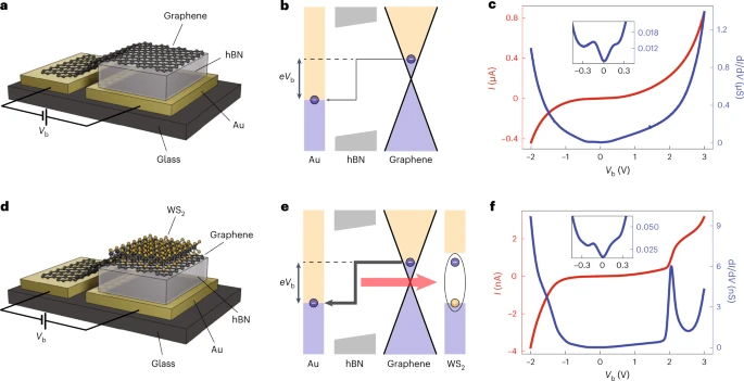
a, Illustration of a graphene/hBN/Au tunnelling device. The device is protected by a top hBN layer (not shown for better visibility). A bias voltage Vb applied between the graphene and gold electrodes gives rise to a tunnelling current through the hBN spacer. b, Band diagram of the device for positive Vb. Electrons tunnel from graphene to Au both elastically (not shown) and inelastically (kinked arrow). c, Recorded I−V (red) and dI/dV (blue) curves at room temperature from the device in a. No distinctive features are observed besides an overall asymmetry due to the electronic density of states in Au. The inset shows a zoom into the low-bias region displaying phonon-assisted resonances. d, Illustration of a WS2/graphene/hBN/Au tunnelling device, which includes a protecting top hBN layer (not shown). e, Band diagram of the device at a positive bias. Electron tunnelling can be mediated by the creation of excitons (encircled electron–hole pair) in WS2, as indicated by the red arrow. f, Recorded I−V (red) and dI/dV (blue) curves at room temperature from the device in d. A new feature appears near Vb = 2.05 V. The inset shows a zoom into the low-bias region displaying phonon-assisted resonances.
As shown in Fig. 1d, we place a TMD monolayer on top of the graphene electrode and investigate its influence on electron tunnelling. To avoid direct tunnelling between the TMD and Au, we place the TMD flake fully inside the graphene area. The band diagram of a WS2-based device is sketched in Fig. 1e for positive bias. Once eVb (e, elementary charge) reaches the exciton energy of WS2, a new inelastic tunnelling channel opens up. It arises from the coupling of tunnelling electrons to WS2 excitons, as indicated by the red arrow. Figure 1f shows the measured I−V dependence (red curve) of the WS2 device. It exhibits a characteristic feature near Vb = 2 V, which is absent in the I−V curve of the reference device (Fig. 1c). We attribute this sudden increase in the tunnelling current to the onset of exciton-assisted resonant tunnelling. Note that this feature is not visible for negative Vb because it is masked by the high current arising from the large electronic density of states associated with 5d electrons in Au (Supplementary Fig. 9). For the same reason, the breakdown voltage of the device is considerably lower for negative Vb and we cannot extend our measurements beyond –2 V. Figure 1f shows the corresponding dI/dV curve (blue). For near-zero bias, it shows phonon-assisted resonances (inset), as in the case of the reference device. In contrast to the reference device, however, we now observe a pronounced resonance peak at ~2.05 V. The energy of 2.05 eV matches well with that of excitonic excitations in monolayer WS2 (refs. 22,23), which provides strong support in favour of the exciton-assisted tunnelling mechanism.
To substantiate our findings, we perform temperature-dependent measurements for devices with different types of TMD monolayers. Our results are shown in Fig. 2a–d for WS2, MoS2, WSe2 and MoSe2. For all of these TMDs, we observe that the resonance becomes sharper and stronger with decreasing temperature, an effect that we attribute to the lower thermal broadening of both the electron distribution in the electrodes28 and the exciton resonance.

a–d, dI/dV measurements for WS2 (a), MoS2 (b), WSe2 (c) and MoSe2 (d) devices at temperatures indicated by the legends.
For the WS2 device, we observe a shift in peak position to larger bias voltages, from ~2.05 V (290 K) to ~2.07 V (10 K), consistent with the temperature-dependent measurements of excitonic resonances in WS2 (refs. 34,35). Upon closer inspection, we find another resonance near 2.26 V, which becomes visible at low temperatures for the WS2 device (Fig. 2a and Supplementary Fig. 6a), suggesting coupling to excitons of higher energy.
Measurements for a MoS2 device are plotted in Fig. 2b, where a main peak at Vb = 2.1 V is observed, exhibiting a similar temperature dependence as the WS2 device. A weak feature appears at slightly lower Vb and develops into two distinct shoulders at lower temperatures, one at ~1.92 V and another one at ~2.02 V (also Supplementary Fig. 6b). The irregular features at bias voltages beyond 2.2 V, especially at high temperatures, can be attributed to measurement instabilities.
For the WSe2 device shown in Fig. 2c, we observe a main resonance at Vb = 1.7 V, and the temperature dependence is similar to the previous two devices. The wiggles appearing at higher bias voltages can be assigned to measurement instabilities (Supplementary Section 3 and Supplementary Figs. 6 and 7). The MoSe2 device plotted in Fig. 2d presents the same temperature behaviour. The resonance in this case appears at Vb = 1.9 V. The smaller feature at ~2.04 V, which becomes more pronounced at low temperatures, likely arises from higher energy excitons. The resonances appear at different bias voltages for every TMD, an observation that hints at exciton coupling.
Further evidence for exciton-assisted electron tunnelling is provided by our electroluminescence (EL) measurements. Excitons generated by resonant electron tunnelling can partially decay through radiative electron–hole recombination. As shown in Fig. 3c, this radiative decay gives rise to a distinctive peak in the measured EL spectrum. Figure 3a illustrates the layout of a MoSe2-based device. Electrons tunnel in the region where graphene, hBN and the Au electrode overlap (the area enclosed by a white dashed line). The MoSe2 monolayer indicated by the red polygon is placed directly above the graphene layer. The upper two electrodes on the left-hand side serve as electrical contacts to graphene. The photograph in Fig. 3b shows that EL is observed when a voltage Vb = 2.5 V is applied. The emission is restricted to the region where the MoSe2 monolayer overlaps with the tunnelling device. Spectra of the emitted light for different bias voltages are plotted in Fig. 3c. The peak centred at ~1.57 eV agrees with previous studies36,37 and can be assigned to the A exciton of MoSe2 according also to our photoluminescence spectroscopy measurements (Supplementary Table 2). Note, however, that the corresponding peak in the differential conductivity measurements shown in Fig. 2d appears at higher voltages than the A exciton energy, suggesting coupling to higher-order excitons. The EL intensity of the other three TMD devices in Fig. 2 is below our detection threshold because we used a considerably thicker hBN spacer to prevent breakdown, so the resulting current densities are more than two orders of magnitude lower than those of the MoSe2 device (Supplementary Fig. 1). Excitonic light emission from a WSe2 device with a thinner hBN tunnel barrier is shown in Supplementary Fig. 5.

a, Optical microscope image of a MoSe2 device fabricated on a glass (SiO2) substrate. The device consists of a vertical stack of a top hBN (t-hBN) protection layer, a MoSe2 monolayer, a graphene (Gr) monolayer, a ~3.3-nm-thick tunnel hBN layer (tnl-hBN) and a Au electrode. The graphene/hBN/Au tunnel junction is indicated by the white dashed line, where the graphene is partially covered by a MoSe2 monolayer (red polygon) on top. The upper two electrodes on the left serve as electrical contacts to the graphene sheet. Scale bar, 10 μm. b, Image of light emitted from the device at an applied voltage of 2.5 V, superimposed on the reference image of the device taken with back illumination. Scale bar, 10 μm. c, EL spectra for different bias voltages. The exciton peak at ~1.57 eV becomes more pronounced with increasing bias voltage.
We continue by theoretically exploring the mechanisms responsible for resonant tunnelling and EL. The tunnelling process involves conservation of both energy and in-plane momentum, for which there is a clear mismatch between graphene and gold, as illustrated in Fig. 4a,b (also Supplementary Fig. 10). In addition, tunnelling favours final electron gold states with a large out-of-plane energy, which reside close to the conduction band of the hBN spacer. Consequently, the momentum of the final states lies near the surface-projected Γ point of the involved materials, as illustrated in Fig. 4b, and also in Supplementary Fig. 10c, where we observe a dramatic depletion of electron spill-out in gold-bound electrons when moving away from the Γ point, corresponding to k∥ = 0 in the space of parallel wave vector k∥. Tunnelling is therefore expected to be dominated by transitions from graphene electrons near the Kg point in this material to gold states near its Fermi level at the surface-projected Γ point, involving a large in-plane wave vector transfer of ~17 nm−1. Phonons can provide such large momentum, and in fact, graphene and hBN have similar in-plane lattice parameters (2% mismatch), so that phonons (frequency ωp) in both materials can assist quasi-elastic tunnelling, giving rise to the features observed at low bias voltages Vb ≈ ħωp/e ≈ 65 mV (ħ, reduced Planck’s constant) in the insets of Fig. 1c,f and in agreement with previous studies14.

a, We consider two possible tunnelling channels under the configuration of Fig. 1d, illustrated here by an on-scale representation of the graphene first Brillouin zone (1BZ; dashed hexagon in the space of parallel wave vector k∥), the surface-projected gold Fermi surface (orange circle, \(k_{\mathrm{F}}^{\mathrm{Au}}\) is the Fermi wave vector of Au) and the TMD 1BZ (colour plot, showing the non-local surface conductivity for MoSe2 at 2.1 eV photon energy). The two channels are (1) one-step tunnelling assisted by the creation of indirect TMD excitons (blue arrow) and (2) two-step tunnelling associated with phonon creation (purple arrow) followed by direct-exciton creation (green arrow). Direct excitons produce the intense feature at the Γ point in the TMD conductivity, while indirect excitons show up as maxima at special regions of the TMD 1BZ, such as the Q point (colour plot, showing the non-local surface conductivity (logarithmic scale) for MoSe2 at 2.1 eV photon energy). b, Gold conduction-band dispersion diagram (orange), along with the energy–momentum region occupied by graphene electrons (light blue), involving a bias energy eVb as well as the gold and graphene Fermi energies \({E}_{{{{\rm{F}}}}}^{{{{\rm{Au}}}}}\) and \({E}_{{{{\rm{F}}}}}^{{{{\rm{g}}}}}\), respectively, out-of-plane electron energy in gold at the Fermi level, \(E_{\mathrm{F}}^{\perp}\). As a function of k∥, the out-of-plane gold Fermi surface (dashed orange parabola) has a minimum energy mismatch (that is, a maximum spill-out of gold electrons towards the hBN barrier) at the Γ point. The two considered tunnelling channels bridge the energy–momentum mismatch between the graphene K point and gold Fermi energy at k∥ = 0. The direction of \({\mathbf{k}}_{\parallel}\) in \({\bf b}\) is along the radial dashed line in \({\bf a}\). c,d, Calculated voltage-dependent tunnelling current associated with one-step indirect TMD exciton creation (c) and two-step phonon plus direct-exciton creation (d) for a hBN tunnel barrier of 3 nm and different TMDs. The insets in c and d show the corresponding dI/dV curves.
We identify two tunnelling mechanisms that can bridge the graphene–gold momentum mismatch, as illustrated by thick arrows in Fig. 4a,b: (1) a single-step process (Iind-ex current) involving the creation of indirect TMD excitons (blue arrow) and (2) a two-step process (Iph+ex current) in which phonons provide the required large in-plane momentum (purple arrow) and direct excitons provide the energy difference between initial and final states (green arrow). A detailed analysis of these channels is provided in Supplementary Notes 6–9, from which we conclude that the associated currents bear a dependence on Vb given by
expressed in terms of the screened interaction WGG′(k∥,z,z′,ω) (ref. 38). This screened interaction is defined as the potential created at a distance z from the gold surface by a unit charge placed at a distance z′, oscillating with frequency ω, and decomposed in parallel wave vectors k∥ within the first Brillouin zone (1BZ) of the TMD, as well as reciprocal lattice vectors G and G′. We set z = z′ = d at the graphene plane (therefore, d corresponds to the graphene-gold spacing), where the initial source of electrons is located. Also, the frequency ω is determined by the associated bias frequency eVb/ħ in Iind-ex, a value that needs to be corrected by the emitted phonon frequency in Iph+ex. The actual expressions that we use to compute the contributions in Fig. 4c,d are slightly more complex, as detailed in the Supplementary Information, but essentially captured by equations (1a) and (1b).
The single-step current Iind-ex (equation (1a)) receives equal contributions from each of the six smallest non-vanishing reciprocal lattice vectors G of the TMD, involving a dominant k∥ value in the 1BZ where the optical conductivity reaches a maximum (colour plot in Fig. 4a). These features are associated with indirect excitons connecting the K point of the TMD with the Q point. Although the relative lattice orientations of TMD and graphene are undefined in our samples, we note that ∣k∥ + G∣ provides the required ~17 nm−1 in-plane wave vector, and in fact, even after averaging over lattice orientations, indirect excitons produce discernible shoulders in the Vb-dependent profile of the resulting current (Fig. 4c), which are better visualized in the dI/dV curves (inset). The single-step indirect-exciton-assisted current thus displays features similar to experiment, although a determination of their detailed energies demands further computations exceeding our current resources. In the two-step tunnelling process (equation (1b)), the screened interaction is evaluated at k∥ = 0 and G = 0, and the resulting current displays direct-exciton features (Fig. 4d), but their strengths relative to the background are small compared to those of the indirect-exciton mechanism.
Since it is revealed that not only phonons but also indirect excitons between K-point valence-band states and Q-point conduction-band states can provide the missing in-plane momentum for tunnelling in our devices, we finalize our study by comparing the peak positions of our dI/dV curves with direct and indirect exciton energies. Supplementary Table 2 includes experimental and calculated values of exciton energies and in-plane momentum values for various TMDs. The Mo-based TMDs present peaks that are higher in energy than A excitons, and they fit well with the reported values of K–Q indirect excitons, suggesting that mostly indirect exciton transitions contribute to the observed resonant tunnelling behaviour. In contrast, K–Q indirect exciton energies in the W-based TMDs are closer to the A exciton energies, and both of them appear near their corresponding dI/dV peak energies, making the distinction between them more difficult. Although a one-step indirect exciton transition is likely to be more efficient, the EL emission from our MoSe2 devices suggests the involvement of direct excitons. Such radiative exciton decay can happen either from the phonon plus direct-exciton transitions or by phonon-assisted luminescence from indirect excitons, as reported in previous studies25.
In conclusion, we have demonstrated exciton-assisted resonant electron tunnelling in graphene/hBN/Au tunnel junctions with a TMD monolayer placed in proximity to the graphene layer. This process manifests as an abrupt increase in the tunnel current when the bias electron energy eVb matches an exciton energy, resulting in a resonance peak in the dI/dV curve. An observed blueshift of the resonant peak with decreasing temperature is consistent with that of the corresponding excitons revealed by optical spectroscopy34,35. We find that the exciton states giving rise to the main resonance peaks in the dI/dV curves are different for the four studied TMD devices. We theoretically explain our measurements by electron tunnelling mechanisms that involve either indirect or direct excitons. Indirect excitons can supply both the energy and in-plane momentum required to tunnel from graphene to gold, while direct excitons require additional in-plane momentum supplied by phonons. Our findings are further substantiated by optical measurements, which reveal excitonic light emission driven by inelastic electron tunnelling. In our devices, the TMD layer is placed outside of the electron tunnelling path, which allows us to suppress exciton generation by direct charge injection, in contrast with previous studies of excitonic emission in tunnel junctions where exciton generation by charge injection cannot be excluded39,40. Finally, this device structure provides a platform not only for studying fundamental aspects of tunnelling processes, but also for exploring novel device functionalities for optoelectronics, all-electrical sensing and spectroscopy.
Methods
Sample fabrication
All flakes are mechanically exfoliated from bulk crystals in air (hBN) or in an argon-based glove box (TMD and graphene). The heterostructures are first assembled using a standard pick-up technique with a polydimethylsiloxane/polycarbonate stamp41, then transferred onto the prefabricated Au electrodes on a glass substrate in the glove box.
Electrical and optical measurements
Room temperature electrical measurements are performed using a Keithley 2602B source meter. Low-temperature measurements are performed in a variable temperature probe station. Currents are measured using a Femto DDPCA-300 current amplifier. An ADwin Pro II data acquisition and control system is used to apply the bias voltage and read the output voltage of the current amplifier. For optical measurements, the samples are mounted on a Nikon TE300 inverted microscope under ambient conditions. The emitted light is collected by a ×100 objective (numerical aperture = 0.9) and analysed using an Andor iXon Ultra camera and a Princeton Instruments Acton SpectraPro 300i spectrometer.
Theoretical calculations
The screened interaction in equation (1) is obtained by combining first-principles calculations of the non-local conductivity of TMD monolayers, the random-phase-approximation non-local response of graphene and the specular-reflection model for the non-local response of the gold surface based on the Lindhard permittivity for the bulk metal. The anisotropic response of hBN is accounted for through a local permittivity tensor. To deal with indirect TMD excitons, the response of the heterostructure is calculated with the inclusion of umklapp processes for the reflection and transmission coefficients of the TMD layer, which permeate the screened interaction, such that it becomes a tensor labelled by TMD reciprocal lattice vectors and wave vectors within the 1BZ. The derivation of equation (1) further involves the analysis of the electron potential landscape in the heterostructure, which is incorporated through the corresponding electron Green function. A detailed self-contained analysis of these elements is presented in Supplementary Notes 6–9, along with graphical information on the TMD non-local conductivities and the screened interaction of our heterostructures.
Data availability
All data presented in Figs. 1–4 are available via the ETH Zürich Research Collection at https://doi.org/10.3929/ethz-b-000607538.
References
Geim, A. K. & Grigorieva, I. V. Van der Waals heterostructures. Nature 499, 419–425 (2013).
Wallbank, J. R. et al. Tuning the valley and chiral quantum state of Dirac electrons in van der Waals heterostructures. Science 353, 575–579 (2016).
Ma, Q. et al. Tuning ultrafast electron thermalization pathways in a van der Waals heterostructure. Nat. Phys. 12, 455–459 (2016).
Yankowitz, M. et al. Emergence of superlattice Dirac points in graphene on hexagonal boron nitride. Nat. Phys. 8, 382–386 (2012).
Wang, L. et al. New generation of moiré superlattices in doubly aligned hBN/graphene/hBN heterostructures. Nano Lett. 19, 2371–2376 (2019).
Cao, Y. et al. Unconventional superconductivity in magic-angle graphene superlattices. Nature 556, 43–50 (2018).
Rivera, P. et al. Observation of long-lived interlayer excitons in monolayer MoSe2–WSe2 heterostructures. Nat. Commun. 6, 6242 (2015).
Koppens, F. H. L. et al. Photodetectors based on graphene, other two-dimensional materials and hybrid systems. Nat. Nanotechnol. 9, 780–793 (2014).
Massicotte, M. et al. Picosecond photoresponse in van der Waals heterostructures. Nat. Nanotechnol. 11, 42–46 (2016).
Withers, F. et al. Light-emitting diodes by band-structure engineering in van der Waals heterostructures. Nat. Mater. 14, 301–306 (2015).
Chynoweth, A. G., Logan, R. A. & Thomas, D. E. Phonon-assisted tunneling in silicon and germanium Esaki junctions. Phys. Rev. 125, 877–881 (1962).
Eaves, L., Guimares, P. S. S., Snell, B. R., Taylor, D. C. & Singer, K. E. Oscillatory structures in GaAs/(AlGa)As tunnel junctions. Phys. Rev. Lett. 55, 262 (1985).
Brar, V. W. et al. Scanning tunneling spectroscopy of inhomogeneous electronic structure in monolayer and bilayer graphene on SiC. Appl. Phys. Lett. 91, 122102 (2007).
Zhang, Y. et al. Giant phonon-induced conductance in scanning tunnelling spectroscopy of gate-tunable graphene. Nat. Phys. 4, 627–630 (2008).
Wehling, T. O., Grigorenko, I., Lichtenstein, A. I. & Balatsky, A. V. Phonon-mediated tunneling into graphene. Phys. Rev. Lett. 101, 216803 (2008).
Vdovin, E. E. et al. Phonon-assisted resonant tunneling of electrons in graphene–boron nitride transistors. Phys. Rev. Lett. 116, 186603 (2016).
Cao, H., Klimovitch, G., Björk, G. & Yamamoto, Y. Direct creation of quantum well excitons by electron resonant tunneling. Phys. Rev. Lett. 75, 1146–1149 (1995).
Cao, S. M. & Willander, M. Exciton-induced tunneling effect on the current-voltage characteristics of resonant tunneling diodes. J. Appl. Phys. 81, 6221–6228 (1997).
Qian, H. et al. Highly-efficient electrically-driven localized surface plasmon source enabled by resonant inelastic electron tunneling. Nat. Commun. 12, 3111 (2021).
Enaldiev, V., Bylinkin, A. & Svintsov, D. Plasmon-assisted resonant tunneling in graphene-based heterostructures. Phys. Rev. B 96, 125437 (2017).
Chandni, U., Watanabe, K., Taniguchi, T. & Eisenstein, J. P. Evidence for defect-mediated tunneling in hexagonal boron nitride-based junctions. Nano Lett. 15, 7329–7333 (2015).
Wang, G. et al. Colloquium: excitons in atomically thin transition metal dichalcogenides. Rev. Mod. Phys. 90, 021001 (2018).
Goryca, M. et al. Revealing exciton masses and dielectric properties of monolayer semiconductors with high magnetic fields. Nat. Commun. 10, 4172 (2019).
Barati, F. et al. Vibronic exciton–phonon states in stack-engineered van der Waals heterojunction photodiodes. Nano Lett. 22, 5751–5758 (2022).
Funk, V. et al. Spectral asymmetry of phonon sideband luminescence in monolayer and bilayer WSe2. Phys. Rev. Res. 3, L042019 (2021).
Meneghini, G., Brem, S. & Malic, E. Ultrafast phonon-driven charge transfer in van der Waals heterostructures. Nat. Sci. 2, e20220014 (2022).
Du, L. et al. Strong and tunable interlayer coupling of infrared-active phonons to excitons in van der Waals heterostructures. Phys. Rev. B 99, 205410 (2019).
Lambe, J. & McCarthy, S. L. Light emission from inelastic electron tunneling. Phys. Rev. Lett. 37, 923–925 (1976).
Parzefall, M. et al. Antenna-coupled photon emission from hexagonal boron nitride tunnel junctions. Nat. Nanotechnol. 10, 1058–1063 (2015).
Parzefall, M. et al. Light from van der Waals quantum tunneling devices. Nat. Commun. 10, 292 (2019).
Kuzmina, A. et al. Resonant light emission from graphene/hexagonal boron nitride/graphene tunnel junctions. Nano Lett. 21, 8332–8339 (2021).
Lee, G.-H. et al. Electron tunneling through atomically flat and ultrathin hexagonal boron nitride. Appl. Phys. Lett. 99, 243114 (2011).
Britnell, L. et al. Electron tunneling through ultrathin boron nitride crystalline barriers. Nano Lett. 12, 1707–1710 (2012).
Hanbicki, A. T., Currie, M., Kioseoglou, G., Friedman, A. L. & Jonker, B. T. Measurement of high exciton binding energy in the monolayer transition-metal dichalcogenides WS2 and WSe2. Solid State Commun. 203, 16–20 (2015).
Jadczak, J. et al. Probing of free and localized excitons and trions in atomically thin WSe2, WS2, MoSe2 and MoS2 in photoluminescence and reflectivity experiments. Nanotechnology 28, 395702 (2017).
Tongay, S. et al. Thermally driven crossover from indirect toward direct bandgap in 2D semiconductors: MoSe2 versus MoS2. Nano Lett. 12, 5576–5580 (2012).
Tonndorf, P. et al. Photoluminescence emission and Raman response of monolayer MoS2, MoSe2, and WSe2. Opt. Express 21, 4908–4916 (2013).
García de Abajo, F. J. Optical excitations in electron microscopy. Rev. Mod. Phys. 82, 209–275 (2010).
Pommier, D. et al. Scanning tunneling microscope-induced excitonic luminescence of a two-dimensional semiconductor. Phys. Rev. Lett. 123, 027402 (2019).
Puchert, R. P. et al. Spectral focusing of broadband silver electroluminescence in nanoscopic FRET-LEDs. Nat. Nanotechnol. 12, 637–641 (2017).
Zomer, P. J., Guimaraes, M. H. D., Brant, J. C., Tombros, N. & van Wees, B. J. Fast pick up technique for high quality heterostructures of bilayer graphene and hexagonal boron nitride. Appl. Phys. Lett. 105, 013101 (2014).
Acknowledgements
We thank M. Luisier, A. Jain, R. Khelifa, S. Shan and P. Karnatak for fruitful discussions. This study was supported by funding from ETH Zurich under ETH grant no. ETH-15 19-1 SYNEMA; ETH Zurich Foundation project no. 2013-08 (11) with a donation from the Stavros Niarchos Foundation; and the Swiss National Science Fund under grant no. 200020_192362. K.W. and T.T. acknowledge support from the Japan Society for the Promotion of Science KAKENHI (grant nos. 19H05790, 20H00354 and 21H05233). M.L.P. acknowledges funding by the Swiss National Science Foundation under Eccellenza Professorial Fellowship no. PCEFP2_203663 and funding by the Swiss State Secretariat for Education, Research and Innovation under contract no. MB22.00076. M.C. acknowledges funding by the Swiss National Science Foundation under the Sinergia grant no. 189924 (Hydronics). F.J.G.d.A. acknowledges funding by the Spanish Ministry of Science and Innovation (PID2020-112625GB-I00 and CEX2019-000910-S), Generalitat de Catalunya (CERCA and AGAUR) and Fundaciós Cellex and Mir-Puig.
Funding
Open access funding provided by Swiss Federal Institute of Technology Zurich.
Author information
Authors and Affiliations
Contributions
L.W., S.P. and L.N. conceived the experiment. L.W. fabricated the devices. L.W. and S.P. performed the measurements. L.W. analysed the data. S.P. and J.H. supported the device fabrication. J.Z. performed the low-temperature measurements with support from M.L.P. and M.C.; S.P. and L.N. helped with the data interpretation. F.I. and F.J.G.d.A. developed the theory, performed numerical calculations and wrote the theoretical discussion. K.W. and T.T. provided the high-quality hBN crystals. L.N. initiated and supervised the project. L.W. and S.P. wrote the paper, and all authors discussed the results and worked on the paper.
Corresponding authors
Ethics declarations
Competing interests
The authors declare no competing interests.
Peer review
Peer review information
Nature Materials thanks Nathaniel Gabor, Liping Yu and the other, anonymous, reviewer(s) for their contribution to the peer review of this work.
Additional information
Publisher’s note Springer Nature remains neutral with regard to jurisdictional claims in published maps and institutional affiliations.
Supplementary information
Supplementary Information
Supplementary Figs. 1–19, Tables 1 and 2 and Discussion.
Rights and permissions
Open Access This article is licensed under a Creative Commons Attribution 4.0 International License, which permits use, sharing, adaptation, distribution and reproduction in any medium or format, as long as you give appropriate credit to the original author(s) and the source, provide a link to the Creative Commons license, and indicate if changes were made. The images or other third party material in this article are included in the article’s Creative Commons license, unless indicated otherwise in a credit line to the material. If material is not included in the article’s Creative Commons license and your intended use is not permitted by statutory regulation or exceeds the permitted use, you will need to obtain permission directly from the copyright holder. To view a copy of this license, visit http://creativecommons.org/licenses/by/4.0/.
About this article

Cite this article
Wang, L., Papadopoulos, S., Iyikanat, F. et al. Exciton-assisted electron tunnelling in van der Waals heterostructures. Nat. Mater. 22, 1094–1099 (2023). https://doi.org/10.1038/s41563-023-01556-7
Received:
Accepted:
Published:
Issue Date:
DOI: https://doi.org/10.1038/s41563-023-01556-7
