
Abstract
Understanding and utilizing novel antiferromagnetic (AFM) materials has been recently one of the central issues in condensed matter physics, as well as in materials science and engineering. The relevant contemporary topics include multiferroicity, topological magnetism and AFM spintronics. The ability to image magnetic domains in AFM materials is of key importance for the success of these exciting fields. While imaging techniques of magnetic domains on the surfaces of ferro-(ferri)magnetic materials with, for example, magneto-optical Kerr microscopy and magnetic force microscopy have been available for a number of decades, AFM domain imaging is a relatively new development. We review various experimental techniques utilizing scanning, optical, and synchrotron X-ray probes to visualize AFM domains and domain walls, and to unveil their physical properties. We also discuss the existing challenges and opportunities in these techniques, especially with further increase of spatial and temporal resolution.
Introduction to AFM domains and domain walls
Ever since using a piece of lodestone (magnetite, Fe3O4) as a compass, ferro-(ferri)magnetism has been of great fascination and practical value for more than two thousand years.1,2,3 In fact, the invention and further development of magnetic recording with ferro-(ferri)magnets has been a key component of the microelectronic revolution for the last century.3 On the other hand, antiferromagnetism, the second basic type of magnetic order, has been known since the 1930s and has been commonly observed in numerous magnetic materials.4 The practical means of combining manipulation and detection of antiferromagnetic (AFM) spins in high-tech devices had remained elusive for a long time, but understanding and utilizing exotic AFM materials have been the central issue of condensed matter physics and materials science and engineering in recent years. Contemporary topics include multiferroicity and topological magnets. Multiferroics are materials with simultaneous presence of magnetic order and ferroelectric polarization, and the novel coupling between magnetism and ferroelectricity in multiferroics can be used for new magnetoelectric technologies.5,6 The gapless topological surface states of topological materials such as Weyl, Dirac, and other nodal semimetals have drawn enormous attention for their unique topological properties such as topologically protected surface Fermi arcs, the chiral anomaly, chiral magnetic effects, giant non-linear optical susceptibilities, and beyond.7,8,9 Magnetic Weyl semimetals promise to uplift the physics to the next level, bringing new and large Hall effects, and exotic spin fluctuations and correlations.10,11,12,13,14 It turns out that many of these multiferroics and topological magnets are AFM.5,10,11,12,14,15,16,17
Spintronics where spin and charge degrees of freedom are mutually coupled and manipulated through crossing conjugate fields (i.e. electric fields for spins and magnetic fields for charges) has been an active research area for the last three decades since the discovery of giant magnetoresistance, and has been well implemented in real devices.18,19,20,21 Traditionally, spintronics utilizes ferro-(ferri)magnets, but AFM spintronics has become highly topical due to the active manipulation of the AFM state and its magnetic textures via spin and charge currents, exemplified by the recently reported switching of AFM domains by the current-induced Néel spin-orbit torque.22 AFM materials, in general, could embody the numerous interesting features beneficial for spintronic applications: they produce no stray fields, so are robust against external magnetic fields and make them suitable for device miniaturization. In addition, AFM materials display ultrafast dynamics in THz ranges, and are capable of generating good spin-current transport with micrometer spin-diffusion lengths.23,24,25,26,27 Note that due to their strong spin-momentum locking, the topological states of topological AFM materials have been actively researched for energy-efficient spintronics with, for example, high charge-current to spin-current conversion efficiency, high electron mobility and long spin diffusion length, large magnetoresistance and efficient spin filtering.28 Finally, a large variety of states with strong electronic correlations, leading to phenomena such as superconductivity, heavy-fermi liquids or colossal magnetoresistance are either emerging out of or competing with AFM order. Thus, in order to acquire better understanding of these exotic states, a closer look at the neighboring AFM phase may be worthwhile.
The ability to image magnetic domains in AFM materials is of key importance for understanding multiferroic and magnetic topological materials and developing AFM spintronics. While imaging techniques of magnetic domains on the surfaces of ferromagnetic materials with, for example, magneto-optical Kerr effect (MOKE) microscopy and magnetic force microscopy (MFM) have been available for a number of decades (see Sections 1 and 2), AFM domain imaging is a relatively new development. Before reviewing the variety of new techniques that can be used to visualize different types of AFM domains, we present an overview of the terms and definitions relevant for this discussion.
-
Domain states and domains. Domain states represent the ordered state associated to the possible orientation or phase of the order parameter. A domain is a region assuming one of the possible domain states. Thus, the former is an abstract concept, whereas the latter is associated to the observable order of a material. A particular sample does not have to exhibit all the possible domain states, and more than one domain within a sample can order according to the same domain state.
-
Orientation domain states and translation domain states. Orientation domain states differ in the orientation of the order parameter and they are uniquely distinct: there is no translation operation that can transfer the magneto-crystalline structure of different orientation domain states into each other. Note that in AFM materials, the choice and orientation of the order parameter are not always obvious because of the zero magnetization. Figure 1a–d show orientation domain states differing in the magnetic modulation direction (a), the spin orientation (b), or cycloidicity—clockwise or counterclockwise or helicity—left or right (d) of the AFM spin arrangements. Translation domain states differ at most in the phase of the order parameter. Because of this, they are also called phase domain states (the term we use in this review). They are not uniquely distinct because the magneto-crystalline structure of different phase domain states can be matched by a sub-lattice-vector translation. Figure 1c shows the meeting of the so-called antiphase domains, a term used for a pair of phase domain states differing by a translation of just half a lattice constant. They can occur in commensurate or incommensurate spin structures and show the simplest type of a 180\(^\circ\) domain wall.
Fig. 1: Various AFM domains and domain walls. 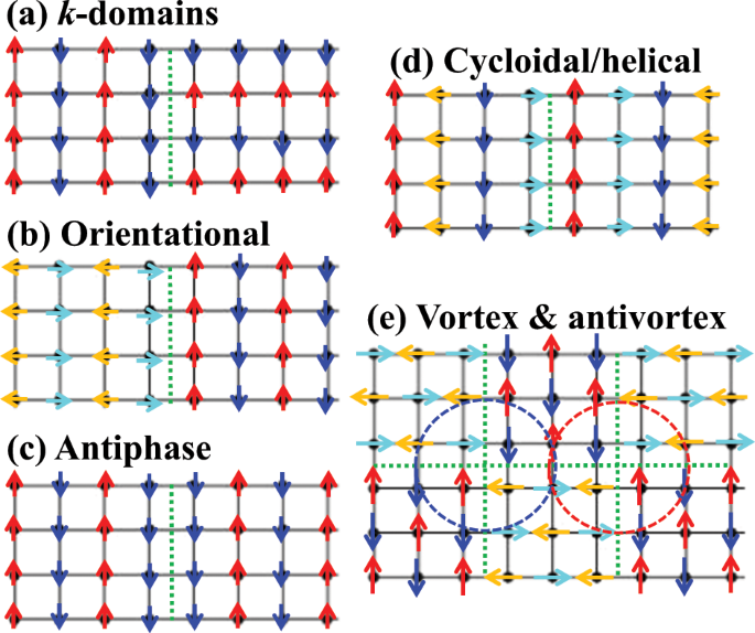
Across a domain wall, a k-type: magnetic modulation direction changes, b orientational: the orientation of AFM spin arrangement changes, c antiphase: a phase shift of AFM order occurs, d cycloidal/helical: cycloidicity (clockwise or counterclockwise) or helicity (left or right) changes, and e AFM vortex/antivortex domains: pairs of AFM vortex and antivortex domains can be present in a large-scale domain/domain wall arrangement.
-
Domains and domain configurations. Whereas a domain is a single, uniformly ordered region of a sample, the domain configuration describes the spatial arrangement of the domains within a sample. In particular, domains may arrange themselves in a vortex- or antivortex-like way around their meeting point if they originate from a topological phase transition. As an example, Fig. 1e shows a Z4-type vortex and antivortex on a square lattice with in-plane spins. AFM Z6 vortex/antivortex domains have been reported in a thin film of α-Fe2O3 (hematite) whereas bulk crystals of α-Fe2O3 do not seem to exhibit them.29,30 The α-Fe2O3 magnetic vortex/antivortex domains resemble crystallographic vortex/antivortex domains observed in, for example, hexagonal R(Mn,Fe) O3 (R = rare earths), Fe1/3TaS2, and Ca2SrTi2O7.31,32,33,34 It is a theoretical and experimental challenge to unveil such AFM vortex/antivortex domains.
-
Domain walls. A domain wall is the region of reorientation of the order parameter at the boundary separating different domains. The domain walls may possess physical or chemical properties very different from those of the bulk interior of the domains because of the chemical mechanical or electromagnetic gradient and confinement occurring at the wall. Note that for a meeting of a specific pair of domains, different types of walls may occur between them. For example, a left- or right-handed spin rotation of the AFM order parameter across a domain wall may may guide the order-parameter reversal.

Subsequent to this classification, we can now focus on various experimental techniques, many of which have been developed in recent years to visualize AFM domains and domain walls. Note that a number of theoretical and experimental issues such as the dynamics, topology, or emergent physical properties of AFM domain walls are recently under active research. In addition, we will briefly comment on the emergent properties of AFM domain walls, distinct from those of AFM domains. We first discuss optical methods like second harmonic generation (SHG) to image AFM domains. SHG works particularly well in magnets with broken inversion symmetry. In the 2nd section, we discuss scanning methods to image AFM domains or domain walls; examples include spin-polarized scanning tunneling microscope (SP-STM) and MFM. In the last section, we discuss AFM domain imaging using synchrotron X-ray techniques such as micro-X-ray diffraction, X-ray magnetic linear dichroism with photo-emission electron microscopy (XMLD-PEEM), and a new and unique method of using coherent soft X-ray to visualize antiphase AFM domains (X-ray Bragg diffraction phase contrast microscopy: XBPM). Note that Lorentz transmission electron microscopy (L-TEM), utilizing the Lorentz force on the incident electron beams, can detect local ferromagnetic moments with a spatial resolution of ∼10 nm, so L-TEM can be used to visualize long-range AFM modulations such as long-wave-length helical spin order.35,36 We also comment that some of these techniques such as the SHG technique rely mostly on domain contrast, some techniques such as XBPM are based on domain wall contrast, and others such as XMLD-PEEM and MFM can result in images with both domain and domain wall contrast. Finally, we present the perspective and challenges of future work on AFM domain/domain wall imaging.
Seeing AFM domains with optical techniques
Access to AFM domains by optical techniques is not obvious since there is no direct coupling between the photon field and the spin. Yet, as early as in the 19th century, the Faraday effect, the Cotton-Mouton effect and the MOKE were introduced as techniques for probing ferromagnetic order and domains.37 All three effects root in magnetic birefringence, usually manifesting as rotation of the plane of polarization of a linearly polarized light wave in interaction with a magnetized medium.
Nevertheless, a variety of optical effects coupling to the AFM order and its domains have been identified over the years.38 We will first discuss linear (frequency-conserving) and then nonlinear (frequency-changing) optical techniques. In the final part, we will discuss the optical detection of dynamical processes involving AFM domains, which is an emerging field of research that benefits from time resolution down to the sub-picosecond range as particular degree of freedom inherent to optical techniques.
Linear optical techniques
Here the term “linear” refers to coherent optical processes that change the amplitude or polarization of a light wave in its interaction with a material, but not its frequency. With very few exceptions, discussed below, linear optical processes do not probe the AFM order directly, but one of its consequences. For example, antiferromagnetism may induce strain into a material via the magnetostrictive or piezomagnetic effect. This strain will manifest as optical birefringence, which distorts the polarization of a light beam transmitted through the sample and is detected with a polarization microscope. In fact, the first observation of purely AFM domains, after these had been predicted to exist by Néel in 1948,39 occurred on NiO in 1960.40 The number of materials displaying strain induced by AFM order is limited, however,41 and the strain may interfere with or even override manifestation of intrinsic AFM behavior. In addition, AFM domain states can only be distinguished via strain if their order parameter points along different crystallographic directions. Most notably, phase domains (differing in the phase φ of the order parameter only) and in particular the ubiquitous spin-reversal domains (or 180° domains because of φ = 180°) cannot be distinguished.42
In a variety of materials, the AFM order may also be accompanied by a macroscopic magnetization in the order of 10–3–10–4 µB. This so-called “weak” or “parasitic” magnetization originates in antisymmetric exchange coupling, the so-called Dzyaloshinskii-Moriya interaction.43,44 The weak magnetic moment is coupled 1:1 to the AFM order parameter, which allows to image AFM domains through the Faraday rotation generated by the weak magnetization. The probably first demonstration occurred on hematite, α-Fe2O3, in 1958. Antiferromagnets exhibiting a parasitic magnetization are restricted to certain symmetry classes, however,34 and despite the smallness of the magnetization, they may behave as ferromagnets rather than antiferromagnets.45
Secondary effects allowing optical detection of the AFM order may also be introduced artificially. A thin ferromagnetic film deposited on an antiferromagnet may experience an effective magnetic field from the coupling to the latter, a phenomenon termed exchange bias.46 Thus, by probing the ferromagnetic order by MOKE, conclusions on the distribution of the AFM domains beneath can be drawn.47
There are also a variety of optical processes with direct coupling to an AFM state that can be regarded as non-magnetization-related complements to the classical magneto-optical effects. Historically, we have the spontaneous nonreciprocal reflection and nonreciprocal directional dichroism. The former denotes a domain-sensitive rotation of the plane of polarization of linearly polarized light in reflection, first observed on Cr2O3,48 a material exhibiting two purely AFM 180° domain states, as sketched in Fig. 2a. With 0.2 mrad (see Fig. 2b) this effect is an order of magnitude smaller than the magnetization-related MOKE in CrO2.49 Recently, a magnetization-less MOKE, likely induced by the material's Berry curvature, was predicted or even observed in Mn3X compounds (X = Rh, Ir, Pt),50,51,52 and an AFM Cotton-Mouton effect has been observed in CuMnAs.53 Nonreciprocal directional dichroism, on the other hand, denotes the dependence of the transmission of a light wave through an AFM crystal on +k or −k as the direction of propagation.54,55,56 Symmetry requirements for MOKE-type optical rotation, nonreciprocal directional dichroism, or SHG (see the next paragraph) in AFM materials are discussed in ref. 57

a Section of the crystallographic unit cell of Cr2O3 with sketch of the AFM Cr3+ order along z in the two opposite 180° domain states. b Spontaneous nonreciprocal reflection measured as circular dichroism as function of temperature on the two domain states. c SHG spectrum of the crystallographic and AFM contributions to SHG. Inset: temperature dependence of the two contributions. d Spatially resolved image of the AFM 180° domain pattern in a z-oriented Cr2O3 sample.66 Scale bar: 1 mm. a reprinted with permission from ref. 123 b reprinted with permission from ref. 48.
Nonlinear optical techniques
The term “nonlinear” refers to coherent optical processes where the interaction with a material involves changes the frequency of the incident light waves.58 The simplest process of this type is SHG. It describes simultaneous absorption of two photons from a light field in the material, followed by the emission of a frequency-doubled light wave. As this process is very unlikely to occur, its observation requires high electromagnetic field strengths, as provided by a pulsed laser.59
In the leading order, SHG is described by the equation Pi(2ω) = ε0χijkEj(ω)Ek(ω) with E as incident light field at frequency ω and P as nonlinear polarization that leaves the material as light wave at 2ω. The rank-three tensor χ as SHG susceptibility parametrizes the light-matter interaction.47 The point-group symmetry of the compound determines the set of allowed tensor components χijk. Any type of ferroic order changes the point symmetry and gives rise to new SHG susceptibilities χijk coupling directly to the order parameter, as depicted in Fig. 2c.41,60,61 Since the process depends on symmetry rather than on the presence of a magnetization, it can detect ferromagnetic and AFM order equally well. In a first experimental demonstration, the AFM order of Cr2O3 was detected by SHG.62 This sensitivity was microscopically explained as the result of low ligand-field symmetry of the Cr3+ ions in combination with spin-orbit interaction.63,64 In spatially resolved SHG measurements, reproduced in Fig. 2d, AFM 180° domain patterns were imaged in Cr2O3, and furthermore in hexagonal YMnO3.65,66,67
Polarization-dependent SHG spectroscopy is particularly useful for studying the coexistence and the magnetoelectric coupling of ferroelectric and AFM domains in multiferroics.67,68,69 SHG even allows to selectively address different coexisting AFM sublattices in a material and analyze their interaction.70 Furthermore, SHG identified ferrotoroidic domains.71,72 Ferrotoroidicity is regarded as a candidate for a fourth form of primary ferroic order that denotes a spontaneous uniform arrangement of magnetic vortices in a material.73 It is closely related to antiferromagnetism by its zero magnetization.
A particular benefit of SHG is its capability to distinguish between AFM 180° and between phase domain states as defined above.61,74 In principle, both of these can be distinguished by polarized neutron diffraction but because of the exposure time of 24 h at a spatial resolution of 100 µm experiments are restricted to very few cases.75 With SHG, the domains are typically imaged in about 1 min and with about 1 µm resolution61,76 so that systematic studies of these hidden and maybe most intrinsic manifestations of AFM domains are now possible. Investigations on a variety of compounds revealed that quite often AFM 180° domains in bulk crystals possess dimensions of >100 µm and no preference to run along specific crystallographic directions. Their manipulation by magnetic fields, electric fields or temperature has been studied in manifold ways.61,69
SHG from opposite AFM 180° domain states differs in the sign of the corresponding SHG light waves only which is equivalent to a 180° phase shift.65 This allows to image opposite domain states as regions of different brightness via an interference technique65 or by the SHG interference between the opposite domain states occurring at the domain walls.76 Even when the lateral size of the AFM domains lies below the resolution limit, statistical information on the topography of the domain pattern can be retrieved from the SHG yield.76 Symmetry requirements for non-zero SHG in normal incidence on arbitrary materials, including AFM compounds are discussed in ref. 57 Furthermore, types of AFM orders possibly exhibiting non-zero SHG are considered.
Magnetization dynamics in antiferromagnets
About 20 years ago, a seminal experiment on nickel demonstrated that the magnetization of a ferromagnet can be significantly reduced by an intense optical pulse within 1 ps and thus, about 100 times faster than expected up to that time.77 This initiated a plethora of studies on ultrafast magnetization dynamics, a field continuing to progress with unbroken attention. Presently, increasing interest is devoted to the dynamical properties of antiferromagnets.78
It was shown that the time scale parameterizing the magnetization dynamics of antiferromagnets may be inherently shorter than that of ferromagnets.79,80 An intense optical pulse may even drive an ultrafast AFM phase transition.80,81 In a conceptual experiment, it was shown that the polarization state of a light wave can be inscribed onto an AFM domain and, following a hold time, retrieved back into a light wave without loss of information.82 AFM domains were furthermore used to generate the inverse effect to the Faraday and the Cotton-Mouton effect and thus create substantial magnetic fields all-optically.83 Finally, reversal of an AFM domain state just by light was demonstrated.84
Imaging AFM domains with scanning probe microscopy
Scanning probe microscopy (SPM) is a powerful analytic tool in materials science. Among various SPM techniques, spin polarized scanning tunneling microscopy (SP-STM),85 magnetic force microscopy (MFM)86 and magnetoelectric force microscopy (MeFM)87 microwave impedance microscopy (MIM)88 have been instrumental in visualizing AFM domains/walls with high spatial resolution. In some extreme case, magnetic exchange force microscopy (MExFM) provide the ultimate atomic resolution of AFM order in insulators.89
SP-STM is a very powerful technique to visualize spin texture with atomic resolution. The atomic resolution of SP-STM is critical to resolve the intrinsic size and internal structure of domain walls in both ferromagnets90,91 and antiferromagnets.85 The principle of SP-STM is the spin dependent tunneling between tip and surface. By functionalizing the STM tip so that its last atom has a well-defined spin polarization, the tunneling probability between tip and sample depends on the relative angle between tip spin and the local spin. In the pioneering work by Bode et al., the atomic spin structure of an antiphase AFM domain wall of monolayer Fe/W (001) was resolved by SP-STM, as shown in Fig. 3a–d.85 However, the strict requirements (atomic flat surface, small domain size, etc.) to realize spin-polarized tunneling limit the application of SP-STM on other AFM materials. Recently SP-STM has been used to visualizing AFM domain walls in some correlated system such as Fe1+yTe and Fe base superconductors.92,93

a Theoretical spin structure. b Simulated, and c experimental SP-STM image of a antiphase domain walls in the out-of-plane antiferromagnetic Fe monolayer on W(001). Scale bar: 300 pm. d Height profiles drawn at the positions of the correspondingly coloured lines in c along the [110] (upper panel) and the [010] (lower panel) direction. Middle panel: sum (black) and difference (gray) of the line profiles shown in the upper panel. The wall is about 1.6 nm wide, and its out-of-plane component exhibits mirror symmetry. Adapted from ref. 85 e Room temperature PFM (top) and low-temperature MFM (bottom) images of the (001) surface of a hexagonal-ErMnO3 single crystal. Scale bar: 1 µm. Adapted from ref. 86 f Room-temperature PFM image on the (001) surface of a hexagonal-ErMnO3 single crystal. Scale bar: 3 µm. g Low-temperature MeFM image taken at the same location as f. Adapted from ref. 87.
The twisting of AFM order parameters at domain walls could result in uncompensated moments, which could be visualized by magnetic imaging techniques. For example, the stray fields of the single layer uncompensated spins on the surface of Cr2O3 were imaged by scanning nitrogen-vacancy (NV) center microscopy, which allowed to measure the reorientation of the AFM order parameter across the domain wall with sub-100 nm spatial resolution.94 This impressive sensitivity to the local magnetization is achieved by attaching a diamond nanocrystal to the atomic force microscopy tip. The NV centers exhibit a Zeeman splitting according to the local magnetic field, which can thus be measured with high magnetic and spatial resolution.
However, most AFM domain walls do not carry uncompensated moments, or the moment size is too small to be detected by typical magnetic imaging techniques. Hexagonal R(Mn,Fe)O3 compounds are a special class of multiferroics, where the trimerization induces Z6 topological vortex domains with alternating ferroelectric polarization. Interestingly, the 120° AFM order of Mn spins couples to the ferroelectric order via the trimerzation mode, resulting in intriguing coupled AFM-ferroelectric domain walls. The winding of the AFM order parameter (120° phase shift) induces alternating canted Mn moments inside domain walls.95 The rare earth elements (e.g. Er) couple to the Mn order, resulting in substantial magnetic moment at the coupled AFM-ferroelectric domain walls.96 In 2012, Geng and coworkers discovered alternating uncompensated magnetic moments at the coupled ferroelectric and AFM domain walls in hexagonal ErMnO3,86 as shown in Fig. 3e, demonstrating that MFM is a powerful tool to reveal emergent phenomena. Recently, AFM topological insulator MnBi2Te4 with alternating ferromagnetic layers (A-type order) has attracted a lot of attention in the condensed matter community.97,98,99 The AFM domain walls of MnBi2Te4 were visualized with cryogenic MFM, revealing micron-size random AFM domains that are stable below the spin-flop transition.100
Another way to visualize AFM domain is to utilize the magnetoelectric responses of special kinds of AFM materials called magnetoelectrics or multiferroics. For magnetoelectrics, linear magnetoelectric response requires breaking both time reversal symmetry and spatial inversion symmetry. The inversion symmetry could be broken by the presence of AFM order. The archetypal example is Cr2O3, which was theoretically predicted to be a magnetoelectric by Dzyaloshinskii.101 Since the magnetoelectric response changes its sign with the phase of AFM domain, it is conceivable to visualize the AFM domains using local magnetoelectric response of the AFM domains. However, the magnetoelectric responses of most magnetoelectrics are either small or become substantial at very low temperatures. Multiferroics are materials where AFM order coexists with ferroelectric polarization. The coupling between these two order parameters could result in large magnetoelectric responses.
In 2014, Geng and coworkers developed a new type of microscopy technique called MeFM, which is a combination of MFM and in situ modulated electric fields, and can be employed to detect the electric-field-induced magnetization.102 Using MeFM, Geng et al. directly observed the local, intrinsic bulk magnetoelectric response of each multiferroic domain in hexagonal ErMnO3, which is in excellent agreement with a symmetry analysis, a microscopic model and first-principles calculations. The magnetoelectric domains coincide with ferroelectric domains, as shown in Fig. 3f, g. Later on, MeFM was demonstrated in imaging AFM domains in archetypal magnetoelectric Cr2O3.95 These pioneering works establish that MeFM is a powerful imaging tool to visualize AFM domains in magnetoelectrics and multiferroics.
For some correlated AFM insulators such as pyrochlore Nd2Ir2O7, the magnetic ordering accompanies a metal-insulator transition. The domain walls of such an AFM compound might host different conduction from domains. As a result, the local conduction contrast can be used to visualize AFM domain walls. In 2015, Ma and collaborators report observation of metallic mobile AFM domain walls in Nd2Ir2O7 using cryogenic MIM.88
Probing AFM domains with synchrotron X-rays
Since the first measurement of X-ray magnetic scattering at the beginning of the 1980s,103,104 probing AFM states and their domain structure with sub-micron resolution has become possible thanks to the multifold increase in spectral brightness at synchrotron sources over the last decades. One can classify the type of studies in three main categories: (1) scattering experiments with a micro- or nano-focused X-ray beam, in the hard or soft X-ray regime, where it is possible to simultaneously spatially resolve the AFM wave-vector and magnetization density, including chirality of the different domains, and in some cases their depth dependence,105 (2) scanning X-ray microscopy and X-ray photo emission electron microscopy (PEEM) both using the absorption contrast produced by magnetic linear dichroism to probe the moment direction along the polarization direction of the incident light, and (3) coherent X-ray imaging in Bragg condition, to image certain types of AFM domains.106
In the hard X-ray regime, and away from atomic resonances, coupling of the photon field to spin and orbital momentum of the electron is intrinsically weak (of the order hν/(mc2), compared to Thomson scattering. Nonetheless, with very bright beams of 3rd and 4th generation synchrotron, it has become possible to study the AFM ordered states of systems even with S = 1/2,107 as long as the signal is not dominated by charge scattering (ideally when the AFM wave-vector lies inside the Brillouin zone). Since the beginning of the 2000s, the progress of micro-focusing optics (Fresnel zone plate and Kirkpatrick-Baez mirror, focusing X-ray beams by reflecting them at grazing incidence off a curved surface, usually coated with a layer of a heavy metal) has opened-up opportunities to spatially resolved magnetic scattering.108 The advantages of the technique are threefold: first, the high momentum resolution allows to separate magnetic reflections belonging to different k-domains, for example in systems with long-wavelength magnetic modulations which break the crystal translational symmetry. Secondly, analyzing the scattered polarization perpendicular to the scattering plane gives access to the moment direction, which is essential to resolve orientation domains. Finally, scattering experiments with circularly polarized light probes chiral magnetic scattering (AFM domains either from cycloidal or helical modulations). Recent studies on a single-domain ferroelectric crystal of BiFeO3109 exploited the aforementioned characteristics to create a topography of the three magnetic k-domains (Fig. 4) and determine the absolute direction of rotation of the cycloids imposed by the electric polarization direction in each domain. Studies on thin films110 are also possible as well as experiments under external perturbations111 (electric, magnetic field). However, in this photon energy range, the penetration of the X-ray beam extends to several microns, preventing the study of systems with domain structures and/or magnetization densities varying rapidly perpendicular to the sample surface. In the last few years, the progress in optics has also driven the construction of hard X-ray nanoprobe beamlines achieving 50 nm spatial resolution by using large transport distance to de-magnify the photon beam size with Kirkpatrick-Baez mirrors. These in principle could be exploited for magnetic studies, but the scientific drivers currently push instead the application towards high resolution elemental mapping in inhomogeneous systems.

a Topography of the magnetic k-domains in rhombohedral BiFeO3 single crystal. Red, blue and green colors represent scattering from each of the 120° domains. The micro-focused beam produces a footprint on the sample of 2 × 2 micron (size of each pixel). b Vector map of the α-Fe2O3 AFM domain configuration from XMLD-PEEEM. It is claimed that it exhibits Z6 vortex/antivortex domains. Scale bar: 2 µm. Adapted from refs. 109,113.
Scattering experiments in resonant conditions enhance dramatically the magnetic contribution and can be used in the hard X-ray and soft X-ray regime, in a similar fashion to what is described in the previous paragraph. Additionally, in the soft regime, it is possible to exploit the large change in absorption at energies close to certain atomic resonance to probe the change in magnetization as of function of depth, virtually impossible to access with other techniques. This was employed successfully recently to probe the magnetization reconstruction of skyrmion lattices close to the surface,105 and could possibly be exploited to access domain information in buried interfaces. Magnetic soft X-ray scattering is unfortunately limited since the Bragg condition can only be satisfied for small momentum transfer (i.e. large periodicity in real space, such as skyrmion lattices, magnetic phases of hexaferrites) due to the low momentum of the photon beam.
In the soft X-ray regime, X-ray magnetic linear dichroism (XMLD) PEEM is a key absorption technique to probe magnetic domains with at the same time an excellent spatial resolution (20–30 nm) and a large field of view (typically 10 μm). Typically, a linearly polarized radiation field is tuned at the L (or M) resonance of the transition metal ion (rare earth ion). The X-ray absorption cross section, dominated by electric dipole terms, includes a resonant magnetic contribution in AFM materials, proportional to the average of the square of local magnetization <M2>. What is detected is the photoemitted electrons (to be precise the secondary electrons emitted in the process) and a magnetic contrast is obtained by subtracting the signals obtained using horizontal and vertical incident polarization. The escape depth of the secondary electrons is typically 6–7 nm, allowing to probe the first few layers of magnetic samples. The electron microscope forms an image with a large field of view in a single shot. Many experiments have been conducted using XMLD-PEEM, which can be performed in a range of temperature down to 10 K, and external stimuli such as current. Recently, the switching of AFM domains by an applied current in metallic CuMnAs has been demonstrated using XMLD-PEEM.112
It is also possible to rotate the sample about the inclined axis the surface makes with the incident direction to create a 3D vector of the magnetization density of each domain. In a recent study, AFM domain configurations in hematite (α-Fe2O3) epitaxial films were observed using 3D vector maps.113 By combining the study with XMCD-PEEM, which probes a net magnetic moment, the authors claimed the presence of Z6 vortex/antivortex domains, imprinted into the magnetization of the ferromagnetic Co layer grown on top of the Fe2O3 film. As noted in the introduction, these Z6 vortex/antivortex magnetic domains are not observed in bulk single crystals of α-Fe2O3.29
As discussed earlier, AFM phase domain states are identical in every respect but the phase of the AFM order parameter. When the phase difference is equal to π, the so-called antiphase domain states and an antiphase domain boundary are realized (see Fig. 1c). Unless the individual atomic spins are measured, a phase-sensitive magnetic probe is needed to image the phase domains. In special cases, when the spins have non-equivalent environments, the antiphase domain states can be distinguished by polarized neutron diffraction topography.114 Hours-long exposures are required, and only ~100 μm-type spatial resolutions are achievable. Non-linear optics techniques, such as the SHG spectroscopy described in this article, also work in special low-symmetry compounds such as Cr2O3.61 Under certain symmetry conditions, phase domains could be distinguished through the circular dichroic charge-magnetic interference effect of resonant X-ray diffraction, and ~10 μm resolutions have been achieved in microbeam scanning experiments.115 All these approaches are based on the interference of the lattice and magnetic signals, and require a favorable combination of low magnetic or structural symmetries. For the general case, however, a probe possessing both phase coherence and direct sensitivity to the AFM order is needed. Magnetic scattering of coherent x rays provides such a probe. A large variety of non-magnetic coherent X-ray imaging techniques exists,116,117,118,119 and many of them should be adaptable for the AFM domain imaging. For direct sensitivity to the AFM order, scattering at non-zero wave vector transfer, such as magnetic Bragg diffraction, is in general needed. The phase domain patterns can be obtained by the detection of domain boundaries using the destructive interference of the magnetic Bragg signals from the adjacent domains.106 In principle, the AFM domains can also be imaged by Fourier transform holography utilizing interference of the incident and the diffracted beams,120 and by several existing coherent diffraction imaging techniques that reconstruct the domain pattern from the observed complex detector images using iterative phase retrieval algorithms.121 Various related approaches utilizing scanning of a nanoscale-sized coherent X-ray beam across the surface of the sample121 should also work. Figure 5 schematically illustrates some of these experimental techniques. While the possibilities are broad, only a very limited amount of work on antiferromagnets has been done so far. Nevertheless, very encouraging initial results have been achieved recently, and the situation could change quickly. As an example, imaging of the antiphase AFM boundaries in a collinear antiferromagnet Fe2Mo3O8 using resonant magnetic Bragg diffraction phase contrast has been demonstrated106—this technique is called X-ray Bragg diffraction phase contrast microscopy (XBPM). In magnetic XBPM, a magnetic Bragg peak, broadened by penetration depth effects, was observed on an area detector. A coherent X-ray beam, producing a circular Airy fringe pattern on the sample surface, gave rise to the similar structure in the Bragg reflection. The antiphase boundaries on the illuminated sample surface were seen as dark lines in the observed detector pattern, producing a direct magnified image of the antiphase domain patterns in a single exposure, see Fig. 5d, e. In these initial XBPM experiments, micron-scale spatial resolutions in mm-sized areas were achieved, and sub-second measurement times were achieved.120 These results demonstrate the promise of coherent X-ray methods for the AFM phase domain imaging. Importantly, the small wavelength of X rays allows for eventual nanometer-scale spatial resolutions. Equally important is the large variety of the possible coherent imaging approaches. In addition to the phase domains, these approaches should also be sensitive to the other AFM domain types described in this paper. As any experimental technique, coherent X-ray scattering has limitations. They are chiefly associated with the necessity to obtain the signal at the scattering vector corresponding to the periodicity of the AFM structure, using the X-ray energy necessary to produce the magnetic resonance. This is not always possible. Another difficulty is the need for high-quality coherent X-ray beams. State-of-the-art coherent scattering facilities are becoming rather widely available at the synchrotron X-ray sources, such as the NSLS-II at Brookhaven National Laboratory. Therefore, significant progress in the imaging of the AFM phase domains using coherent X-ray techniques is expected in the near future.

a Fourier transform (FT) holography utilizing interference of the reference beam with the beam diffracted at the AFM wave vector. b Coherent diffractive imaging. This technique utilizes complex iterative image reconstruction algorithms. In the variation of this approach called ptychography, the beam is scanned on the sample surface, producing overlapping images. Such oversampling leads to more efficient algorithms. c serves as a placeholder reminding that while similar approaches are known to work for structural and ferromagnetic domain imaging, they remain to be realized for the AFM domains. d AFM phase domain imaging based on the detection of domain boundaries in the image of a magnetic Bragg peak. A broad structured coherent beam covers many domain boundaries. Due to the destructive interference, the boundaries are imaged on the detector as dark lines. e 180° AFM domain boundaries (dark wavy lines) observed in the wings of the (001) magnetic peak in a collinear antiferromagnet Fe2Mo3O8 (left), and the corresponding antiphase AFM domain pattern (right).
Perspectives and challenges
We have discussed various experimental techniques to visualize AFM domains and domain walls, and to unveil their physical properties. We now discuss the perspectives and challenges of future work on AFM domains/domain walls.
A large number of types of AFM domains can be visualized by microscopy techniques using MOKE-type optical rotation and/or SHG.57 These techniques, possibly with enhanced spatial resolution, for example by employing near fields, will be further utilized to explore AFM domains and domain walls and large-scale domain configurations of new AFM states. Resolving the magnetic dynamics of AFM materials and, in particular, of magnetoelectric correlation effects in multiferroics is still a much underrated topic. How fast does the AFM order parameter switch and by which mechanism exactly? This question is particularly important for magnetoelectric correlation effects in multiferroics or in AFM spintronics.23 Lack of an answer is surprising as any application of antiferromagnetism inevitably involves the temporal manipulation of the AFM order. Understanding and control of this manipulation requires an intimate knowledge of the temporal progression of the AFM order which therefore needs to be studied. Here, optical experiments will play the key role in the future because of the unparalleled time resolution down to the few-femtosecond range. Aside from the AFM coupling within a material, the coupling at or across the interface between different constituents can add valuable functionalities to the field of oxide electronics. Therefore, the AFM order, domains and domain walls in thin films and heterostructures will catch increasing interest in the future. Here, nonlinear optical techniques will prove useful in two ways. First, they are the ideal tool to resolve AFM domains as well as the coexistence of different types of ferroic domains and the coupling in between them. Second, techniques like SHG allow to monitor the growth of a multilayer heterostructure remotely, and thus while the structure is assembled in the vacuum chamber. The emergence of the oxide functionalities, including antiferromagnetism, can therefore be monitored while they emerge during this layer-by-layer assembly.122 Any processes involving the magnetoelectric order and correlations during the growth and that would be inaccessible in a post-growth ex-situ characterization can therefore be identified. In situ SHG will therefore play an important in tailoring the desired functionalities of a magnetoelectric oxide heterostructure exactly to the needs of the user.
The ultimate spatial resolution of SPM is limited the size of atom at the end of SPM tip, which can be achieved by SP-STM and MeFM. However, the strict requirements (ultra-clean and atomic flat surface) for these imaging techniques severely limit their application on real materials. The functional properties of atomic force microscopy, e.g. in spintronics, are controlled by domains or domain walls. For them, SPMs with sub-micron spatial resolution (e.g. MFM, MeFM, and MIM) are less surface sensitive, and thus are more relevant. The nature of these techniques is such that phase domains cannot be resolved directly. In specific cases, it may be possible to detect the domain walls instead, if the magnetization direction contrasts with the domains themselves, and for certain wall thicknesses.
XMLD-PEEM has a bright future, alongside the recent development in coherent diffraction imaging techniques, as the step-change in technologies continue to drive improvements in resolution and fast acquisition. On one hand, the new generation of direct electron detectors can acquire images at kHz rates. Also, aberration-corrected PEEM instruments are now commercially available and will push the spatial resolution towards 10 nm or increase throughput and image sensitivity dramatically at current resolutions (20–30 nm).
The spatial resolution for the existing phase domain imaging based on the detection of the domain boundaries by coherent X-ray diffraction is limited by the size of the central maximum of the beam footprint on the sample surface. For the pinhole optics, this limits the observable domain size to the micron scales. Focusing elements, such as Fresnel zone plates, should significantly improve the achievable resolutions, potentially to the 10-nm scale.
Further increase of spatial and temporal resolution of these optical/scanning/X-ray techniques will be quintessential for the next step in scientific understanding and technological exploitation of magnetic quantum materials such as spintronic antiferromagnets, multiferroics and magnetic topological materials.
Data availability
The datasets generated during the current study are available from the corresponding author on reasonable request.
References
Lowrie, W. Fundamentals of Geophysics. (Cambridge Univ. Press, Cambridge, 2007).
Du Trémolet de Lacheisserie, E., Gignoux, D. & Schlenker, M. Magnetism: Fundamentals. (Springer, New York, 2005).
Daniel, E. D., Mee, C. D. & Clark, M. H. Magnetic Recording: The First 100 Years. (IEEE Press, New Jersey, 1999).
Néel, L. Nobel Lectures in Physics 1963–1970 318–341 (Elsevier, Amsterdam, 1972).
Cheong, S.-W. & Mostovoy, M. Multiferroics: a magnetic twist for ferroelectricity. Nat. Mater. 6, 13–20 (2007).
Manipatruni, S. et al. Scalable energy-efficient magnetoelectric spin-orbit logic. Nature 565, 35–42 (2019).
Herring, C. Accidental degeneracy in the energy bands of crystals. Phys. Rev. 52, 365–373 (1937).
Murakami, S. Phase transition between the quantum spin Hall and insulator phases in 3D: emergence of a topological gapless phase. N. J. Phys. 9, 356 (2007).
Xu, S. Y. et al. Discovery of a Weyl fermion semimetal and topological Fermi arcs. Science 349, 613–617 (2015).
Nakatsuji, S., Kiyohara, N. & Tomoya, H. Large anomalous Hall effect in a non-collinear antiferromagnet at room temperature. Nature 527, 212–215 (2015).
Kuroda, K. et al. Evidence for magnetic Weyl fermions in a correlated metal. Nat. Mater. 16, 1090–1095 (2017).
Kiyohara, N., Tomita, T. & Nakatsuji, S. Giant anomalous Hall effect in the chiral antiferromagnet Mn3Ge. Phys. Rev. Appl. 5, 064009 (2016).
Chang, G. et al. Magnetic and noncentrosymmetric Weyl fermion semimetals in the RAlGe family of compounds (R=rare earth). Phys. Rev. B 97, 041102 (2018).
Manna, K. et al. Heusler, Weyl and Berry. Nat. Rev. Mater. 3, 244–256 (2018).
Hodovanets, H. et al. Single-crystal investigation of the proposed type-II Weyl semimetal CeAlGe. Phys. Rev. B 98, 245132 (2018).
Hirschberger, M. et al. The chiral anomaly and thermopower of Weyl fermions in the half-Heusler GdPtBi. Nat. Mater. 15, 1161–1165 (2016).
Zhang, D. et al. Topological axion states in the magnetic insulator MnBi2Te4 with the quantized magnetoelectric effect. Phys. Rev. Lett. 122, 206401 (2019).
Cheong, S.-W., Thompson, J. D. & Fisk, Z. Metamagnetism in La2CuO4. Phys. Rev. B 39, 4395–4398 (1989).
Chappert, C., Fert, A. & Van Dau, F. N. The emergence of spin electronics in data storage. Nat. Mater. 6, 813–823 (2007).
Brataas, A., Kent, A. D. & Ohno, H. Current-induced torques in magnetic materials. Nat. Mater. 11, 372–381 (2012).
Kent, A. D. & Worledge, D. C. A new spin on magnetic memories. Nat. Nanotechnol. 10, 187–191 (2015).
Wadley, P. et al. Electrical switching of an antiferromagnet. Science 351, 587–591 (2016).
MacDonald, A. H. & Tsoi, M. Antiferromagnetic metal spintronics. Philos. Trans. R. Soc. A 369, 3098–3114 (2011).
Gomonay, E. V. & Loktev, V. M. Spintronics of antiferromagnetic systems. Low. Temp. Phys. 40, 17–35 (2014).
Jungwirth, T., Marti, X., Wadley, P. & Wunderlich, J. Antiferromagnetic spintronics. Nat. Nanotechnol. 11, 231–241 (2016).
Gomonay, O. et al. Antiferromagnetic spin textures and dynamics. Nat. Phys. 14, 213–216 (2018).
Marrows, C. Addressing an antiferromagnetic memory. Science 351, 558–559 (2016).
Šmejkal, L. et al. Topological antiferromagnetic spintronics. Nat. Phys. 14, 242–251 (2018).
Chmiel, F. P. et al. Observation of magnetic vortex pairs at room temperature in a planar α-Fe2O3/Co heterostructure. Nat. Mater. 17, 581–585 (2018).
Williams, H. J., Sherwood, R. C. & Remeika, J. P. Magnetic domains in α−Fe2O3. J. Appl. Phys. 29, 1772–1773 (1958).
Choi, T. et al. Insulating interlocked ferroelectric and structural antiphase domain walls in multiferroic YMnO3. Nat. Mater. 9, 253–258 (2010).
Du, K. et al. Vortex ferroelectric domains, large-loop weak ferromagnetic domains, and their decoupling in hexagonal (Lu, Sc)FeO3. npj Quantum Mater. 3, 33 (2018).
Horibe, Y. et al. Color Theorems, chiral domain topology, and magnetic properties of FexTaS2. J. Am. Chem. Soc. 136, 8368–8373 (2014).
Huang, F.-T. et al. Topological defects at octahedral tilting plethora in bi-layered perovskites. npj Quantum Mater. 1, 16017 (2016).
Grundy, P. J. & Tebble, R. S. Lorentz electron microscopy. Adv. Phys. 17, 153–242 (1968).
Togawa, Y. et al. Chiral magnetic soliton lattice on a chiral helimagnet. Phys. Rev. Lett. 108, 107202 (2012).
Zvezdin, A. K., Kotov & V. A. Modern magnetooptics and magnetooptical materials. (CRC Press, New York, 1997).
Eremenko, V. V., Kharchenko, N. F., Litvinenko Y. G. & Naumenko V. M. Magneto-optics and Spectroscopy of Antiferromagnets. (Spinger, Berlin, 1992).
Néel, L. Propriétés magnétiques des ferrites. Ferrimagnétisme et antiferromagnétisme. Ann. Phys. 3, 137–198 (1948).
Roth, W. L. Neutron and optical studies in NiO. J. Appl. Phys. 31, 2000–2011 (1960).
Aizu, K. Possible species of ferromagnetic, ferroelectric, and ferroelastic crystals. Phys. Rev. B 2, 754–772 (1970).
Wadhawan, V. K. Introduction to Ferroic Materials. (CRC Press, London, 2000).
Dzyaloshinskii, I. A thermodynamic theory of “weak” ferromagnetism of antiferromagnetics. J. Phys. Chem. Solids 4, 241–255 (1958).
Moriya, T. Anisotropic superexchange interaction and weak ferromagnetism. Phys. Rev. 120, 91–98 (1960).
Wang, W. et al. Visualizing weak ferromagnetic domains in multiferroic hexagonal ferrite thin film. Phys. Rev. B 95, 134443 (2017).
Meiklejohn, W. H. & Bean, C. P. New magnetic anisotropy. Phys. Rev. 105, 904–913 (1957).
Shiratsuchi, Y., Watanabe, S., Yonemura, S., Shibata, T. & Nakatani, R. Frustration and relaxation of antiferromagnetic domains reversed by magneto-electric field cooling in a Pt/Co/Au/Cr2O3/Pt-stacked film. AIP Adv. 8, 125313 (2018).
Krichevtsov, B. B., Pavlov, V. V., Pisarev, R. V. & Gridnev, V. N. Spontaneous non-reciprocal reflection of light from antiferromagnetic Cr2O3. J. Phys. Condens. Matter 5, 8233–8244 (1993).
Kunes, J. et al. Electronic structure of CrO2 as deduced from its magneto-optical Kerr spectra. Phys. Rev. B 65, 165105 (2002).
Chen, H., Niu, Q. & MacDonald, A. H. Anomalous Hall effect arising from noncollinear antiferromagnetism. Phys. Rev. Lett. 112, 017205 (2014).
Feng, W., Guo., G.-Y., Zhou, J., Yao, Y. & Niu, Q. Large magneto-optical Kerr effect in noncollinear antiferromagnets Mn3X (X=Rh, Ir, Pt). Phys. Rev. B 92, 144426 (2015).
Higo, T. et al. Large magneto-optical Kerr effect and imaging of magnetic octupole domains in an antiferromagnetic metal. Nat. Photonics 12, 73–78 (2018).
Saidl, V. et al. Optical determination of the Neel vector in a CuMnAs thin-film antiferromagnet. Nat. Photonics 11, 91–96 (2017).
Figotin, A. & Vitebsky, I. Nonreciprocal magnetic photonic crystals. Phys. Rev. E 63, 066609 (2001).
Arima, T. Non-reciprocal directional dichroism as an extension of the magneto-electric effect. J. Magn. Soc. Jpn 27, 1111–1116 (2003).
Toyoda, S. et al. One-way transparency of light in multiferroic CuB2O4. Phys. Rev. Lett. 115, 267207 (2015).
Cheong, S.-W. SOS: symmetry operational similarity. npj Quantum Mater. 4, 53 (2019).
Shen, Y. R. The Principles of Nonlinear Optics. (John Wiley & Sons. Inc, New Jersey, 2002).
Franken, P. A., Hill, A. E., Peters, C. W. & Weinreich, G. Generation of optical harmonics. Phys. Rev. Lett. 7, 118–119 (1961).
Birss, R. R. Symmetry and Magnetism. (North-Holland Pub., Amsterdam, 1966).
Fiebig, M., Pavlov, V. V. & Pisarev, R. V. Second harmonic generation as a tool for studying electronic and magnetic structures of crystals. J. Opt. Soc. Am. B 22, 96–118 (2005).
Fiebig, M., Fröhlich, D., Krichevtsov, B. B. & Pisarev, R. V. Second harmonic generation and magnetic-dipole-electric-dipole interference in antiferromagnetic Cr2O3. Phys. Rev. Lett. 73, 2127–2130 (1994).
Muthukumar, V. N., Valentí, R. & Gros, C. Microscopic model of nonreciprocal optical effects in Cr2O3. Phys. Rev. Lett. 75, 2766–2769 (1995).
Tanabe, Y., Muto, M., Fiebig, M. & Hanamura, E. Interference of second harmonics due to electric and magnetic dipoles in antiferromagnetic Cr2O3. Phys. Rev. B 58, 8654–8666 (1998).
Fiebig, M., Fröhlich, D., Lottermoser, Th & Kallenbach, S. Phase-resolved second-harmonic imaging with non-ideal laser sources. Opt. Lett. 29, 41–43 (2004).
Fiebig, M., Fröhlich, SluytermanV. L. G. & Pisarev, R. V. Domain topography of antiferromagnetic Cr2O3 by second harmonic generation. Appl. Phys. Lett. 66, 2906–2908 (1995).
Fiebig, M., Lottermoser, Th, Fröhlich, D., Goltsev, A. V. & Pisarev, R. V. Observation of coupled magnetic and electric domains. Nature 419, 818–820 (2002).
Matsubara, M. et al. Magnetoelectric domain control in multiferroic TbMnO3. Science 348, 1112–1115 (2015).
Leo, N. et al. Magneto-electric inversion of domain patterns. Nature 560, 466–470 (2018).
Pisarev, R. V., Sänger, I., Petrakovskii, G. A. & Fiebig, M. Magnetic-field-induced second harmonic generation in CuB2O4. Phys. Rev. Lett. 93, 037204 (2004).
Van Aken, B. B., Rivera, J. P., Schmid, H. & Fiebig, M. Observation of ferrotoroidic domains. Nature 449, 702–705 (2007).
Zimmermann, A. S., Meier, D. & Fiebig, M. Ferroic nature of magnetic toroidal order. Nat. Commun. 5, 4796 (2014).
Spaldin, N. A., Fiebig, M. & Mostovoy, M. The toroidal moment in condensed-matter physics and its relation to the magnetoelectric effect. J. Phys.: Condens. Matter. 20, 434203 (2008).
Meier, D. et al. Observation and coupling of domains in a spin-spiral multiferroic. Phys. Rev. Lett. 102, 107202 (2009).
Schlenker, M. & Baruchel, J. Possibilities of X-ray and neutron topography for domain and phase coexistence observations. Ferroelectrics 162, 299–306 (2011).
Fiebig, M., Fröhlich, D., Lottermoser, Th & Maat, M. Probing of ferroelectric surface and bulk domains in ferroelectric RMnO3 (R=Y, Ho) by second harmonic generation. Phys. Rev. B 66, 144102 (2002).
Beaurepaire, E., Merle, J.-C., Daunois, A. & Bigot, J.-Y. Ultrafast spin dynamics in ferromagnetic nickel. Phys. Rev. Lett. 76, 4250–4253 (1996).
Němec, P., Fiebig, M., Kampfrath, T. & Kimel, A. V. Antiferromagnetic opto-spintronics. Nat. Phys. 14, 229–241 (2018).
Satoh, T., Van Aken, B. B., Duong, N. P., Lottermoser, Th & Fiebig, M. Ultrafast spin and lattice dynamics in antiferromagnetic Cr2O3. Phys. Rev. B 75, 155406 (2007).
Kimel, A. V., Kirilyuk, A., Tsvetkov, A., Pisarev, R. V. & Rasing, T. Laser-induced ultrafast spin reorientation in the antiferromagnet TmFeO3. Nature 429, 850–853 (2004).
Duong, N. P., Satoh, T. & Fiebig, M. Ultrafast manipulation of antiferromagnetism of NiO. Phys. Rev. Lett. 93, 117402 (1994).
Satoh, T., Iida, R., Higuchi, T., Fiebig, M. & Shimura, T. Writing and reading of an arbitrary optical polarization state in an antiferromagnet. Nat. Photonics 9, 25–29 (2015).
Kimel, A. V. et al. Ultrafast non-thermal control of magnetization by instantaneous photomagnetic pulses. Nature 435, 655–657 (2005).
Manz, S. et al. Reversible optical switching of antiferromagnetism in TbMnO3. Nat. Photonics 10, 653–656 (2016).
Bode, M. et al. Atomic spin structure of antiferromagnetic domain walls. Nat. Mater. 5, 477–481 (2006).
Geng, Y., Lee, N., Choi, Y. J., Cheong, S.-W. & Wu, W. Collective magnetism at multiferroic vortex domain walls. Nano Lett. 12, 6055–6059 (2012).
Geng, Y. et al. Direct visualization of magnetoelectric domains. Nat. Mater. 13, 163–167 (2014).
Ma, E. Y. et al. Mobile metallic domain walls in an all-in-all-out magnetic insulator. Science 350, 538–541 (2015).
Kaiser, U., Schwarz, A. & Wiesendanger, R. Magnetic exchange force microscopy with atomic resolution. Nature 446, 522–525 (2007).
Pratzer, M. et al. Atomic-scale magnetic domain walls in quasi-one-dimensional Fe nanostripes. Phys. Rev. Lett. 87, 127201 (2001).
Kubetzka, A., Pietzsch, O., Bode, M. & Wiesendanger, R. Spin-polarized scanning tunneling microscopy study of 360° walls in an external magnetic field. Phys. Rev. B 67, 020401(R) (2003).
Enayat, M. et al. Real-space imaging of the atomic-scale magnetic structure of Fe1+yTe. Science 345, 653–656 (2014).
Choi, S. et al. Switching magnetism and superconductivity with spin-polarized current in iron-based superconductor. Phys. Rev. Lett. 119, 227001 (2017).
Appel, P. et al. Nanomagnetism of magnetoelectric granular thin-film antiferromagnets. Nano Lett. 19, 1682–1687 (2019).
Schoenherr, P. et al. Magnetoelectric force microscopy on sntiferromagnetic 180° domains in Cr2O3. Mater. (Basel) 10, 1051 (2017).
Artyukhin, S., Delaney, K. T., Spaldin, N. & Mostovoy, M. Landau theory of topological defects in multiferroic hexagonal manganites. Nat. Mater. 13, 42–49 (2014).
Gong, Y. et al. Experimental realization of an intrinsic magnetic topological insulator. Chin. Phys. Lett. 36, 076801 (2019).
Otrokov, M. M. et al. Unique thickness-dependent properties of the van der Waals interlayer antiferromagnetic MnBi2Te4 films. Phys. Rev. Lett. 122, 107202 (2019).
Yang, J.-Q. et al. Crystal growth and magnetic structure of MnBi2Te4. Phys. Rev. Mater. 3, 064202 (2019).
Sass, P. M. et al. Magnetic imaging of antiferromagnetic domain walls. Preprint at https://arxiv.org/abs/1910.06488 (2019).
Dzyaloshinskii, I. E. On the magneto-electrical effect in antiferromagnetics. Zh. Exp. Teoret. Fiz 33, 881–882 (1959). [JETP 10, 628–629 (1960)].
Geng, Y. & Wu, W. Magnetoelectric force microscopy based on magnetic force microscopy with modulated electric field. Rev. Sci. Instrum. 85, 053901 (2014).
Brunel, M. & Debergevin, F. Diffraction of X-rays by magnetic materials. II. measurements on antiferromagnetic Fe2O3. Acta Crystallogr. A 37, 324–331 (1981).
Debergevin, F. & Brunel, M. Diffraction of X-rays by magnetic materials. I. general formulae and measurements on ferro- and ferrimagnetic compounds. Acta Crystallogr. A 37, 314–324 (1981).
Zhang, S. et al. Reciprocal space tomography of 3D skyrmion lattice order in a chiral magnet. Proc. Natl Acad. Sci. USA 115, 6386–6391 (2018).
Kim, M. G. et al. Imaging antiferromagnetic antiphase domain boundaries using magnetic Bragg diffraction phase contrast. Nat. Commun. 9, 5013 (2018).
Johnson, R. D. et al. Cu3Nb2O8: a multiferroic with chiral coupling to the crystal structure. Phys. Rev. Lett. 107, 137205 (2011).
Evans, P. G. X-ray Microdiffraction images of antiferromagnetic domain evolution in chromium. Science 295, 1042–1045 (2002).
Johnson, R. D. et al. X-ray imaging and multiferroic coupling of cycloidal magnetic domains in ferroelectric monodomain BiFeO3. Phys. Rev. Lett. 110, 217206 (2013).
Price, N. et al. Coherent magnetoelastic domains in multiferroic BiFeO3 films. Phys. Rev. Lett. 117, 177601 (2016).
Fabrizi, F. et al. Electric field control of multiferroic domains in Ni3V2O8 imaged by X-ray polarization-enhanced topography. Phys. Rev. B. 82, 024434 (2010).
Wadley, P. et al. Electrical switching of an antiferromagnet. Science 351, 587–590 (2016).
Chmiel, F. P. et al. Observation of magnetic vortex pairs at room temperature in a planar α-Fe2O3 /Co heterostructure. Nat. Mater. 17, 581–585 (2018).
Dobrzynski, L. & Binowski, K. Neutrons and Solid State Physics (Ellis Horwood, London, 1994).
Ueda, H., Tanaka, Y., Wakabayashi, Y. & Kimura, T. Observation of collinear antiferromagnetic domains making use of the circular dichroic charge-magnetic interference effect of resonant X-ray diffraction. Phys. Rev. B 98, 134415 (2018).
Mayo, S. C., Stevenson, A. W. & Wilkins, S. W. In-line phase-contrast X-ray imaging and tomography for materials science. Materials 5, 937–965 (2012).
Nugent, K. A. Coherent methods in the X-ray sciences. Adv. Phys. 59, 1–99 (2010).
Cloetens, P., Barrett, R., Baruchel, J., Guigay, J. P. & Schlenker, M. Phase objects in synchrotron radiation hard X-ray imaging. J. Phys. D.: Appl. Phys. 29, 133–146 (1996).
Miao, J., Ishikawa, T., Robinson, I. K. & Murnane, M. M. Beyond crystallography: diffractive imaging using coherent X-ray light sources. Science 348, 530–535 (2015).
Eisebitt, S. et al. Lensless imaging of magnetic nanostructures by X-ray spectro-holography. Nature 432, 885–888 (2004).
Tripathi, A. et al. Dichroic coherent diffractive imaging. Proc. Natl Acad. Sci. USA 108, 13393–13398 (2011).
De Luca, G. et al. Nanoscale design of polarization in ultrathin ferroelectric heterostructures. Nat. Commun. 8, 1419 (2017).
Artman, J. O. & Murphy, J. C. Symmetry considerations in the spectrum of ruby. J. Chem. Phys. 38, 1544–1547 (1963).
Acknowledgements
S.W.C. and V.K. were supported by the DOE under Grant No. DOE: DE-FG02–07ER46382. W.W. is supported by the U.S. Department of Energy (DOE) Office of Science, Basic Energy Sciences (BES) under Award # DE-SC0018153. MF was supported by the SNSF grant 178825 and by the ERC Advanced Grant INSEETO (No. 694955). We thank Kefeng Wang for proofreading the paper.
Author information
Authors and Affiliations
Contributions
All authors wrote the paper together.
Corresponding author
Ethics declarations
Competing interests
The authors declare no competing interests.
Additional information
Publisher’s note Springer Nature remains neutral with regard to jurisdictional claims in published maps and institutional affiliations.
Rights and permissions
Open Access This article is licensed under a Creative Commons Attribution 4.0 International License, which permits use, sharing, adaptation, distribution and reproduction in any medium or format, as long as you give appropriate credit to the original author(s) and the source, provide a link to the Creative Commons license, and indicate if changes were made. The images or other third party material in this article are included in the article’s Creative Commons license, unless indicated otherwise in a credit line to the material. If material is not included in the article’s Creative Commons license and your intended use is not permitted by statutory regulation or exceeds the permitted use, you will need to obtain permission directly from the copyright holder. To view a copy of this license, visit http://creativecommons.org/licenses/by/4.0/.
About this article

Cite this article
Cheong, SW., Fiebig, M., Wu, W. et al. Seeing is believing: visualization of antiferromagnetic domains. npj Quantum Mater. 5, 3 (2020). https://doi.org/10.1038/s41535-019-0204-x
Received:
Accepted:
Published:
DOI: https://doi.org/10.1038/s41535-019-0204-x
This article is cited by
-
Topological surface magnetism and Néel vector control in a magnetoelectric antiferromagnet
npj Quantum Materials (2023)
-
Scanning gradiometry with a single spin quantum magnetometer
Nature Communications (2022)
-
Ultrafast reorientation of the Néel vector in antiferromagnetic Dirac semimetals
npj Computational Materials (2021)
-
Nanoscale mechanics of antiferromagnetic domain walls
Nature Physics (2021)
-
Discovery and characterization of a new type of domain wall in a row-wise antiferromagnet
Nature Communications (2021)
