
Abstract
Transparent conductors with electromagnetic shielding capabilities (TC-EMS) are rare, despite their significant potential for creating new functionalities in energy and military applications. Here, we investigate the potential of La-doped BaSnO3 (BLSO) for TC-EMS since its epitaxial film has been known to have low sheet resistance and high visible transmittance. However, films grown on industrially practical Al2O3 substrates exhibit a sheet resistance three orders of magnitude higher than that of reported films grown on perovskites. Here, this problem is addressed by templating a BaZrO3/MgO bilayer on (0001)-oriented Al2O3 substrates to yield single-crystalline BLSO epitaxial films. The absence of grain boundaries in the epitaxial films minimizes the electron scattering. Due to the affirmative correlation between the conductivity and crystallinity, 5% La doping is optimal among the 5−20% La concentrations studied; these 480-nm-thick films have the highest crystallinity and the lowest sheet resistances of ~28 Ω ▯−1; this value is similar to that of single-crystalline levels. Due to their very high transmittances (~82% in a range 400−1000 nm) and effective X-band electromagnetic shielding (~18.6 dB), the BLSO epitaxial films grown on Al2O3 have great potential to be used for inexpensive TC-EMS applications.
Introduction
The development of transparent conductors with electromagnetic shielding capabilities (TC-EMS) has thrived in multidisciplinary fields, such as human health care, invisible circuits, and neutralizing military stealth technology1,2,3,4,5,6,7,8,9,10. For excellent TC-EMS performance, the relevant materials should simultaneously satisfy a low sheet resistance (<200 Ω ▯−1), high visible transmittance (>50% at a wavelength of 550 nm), and high electromagnetic shielding effectiveness (>20 dB at 10 GHz in the X-band). Although many materials have been tested for TC-EMS, they have encountered many issues. Highly conducting metal films with EMS usually show weak light transmittance. Irrespective of the light transmittance, metal nanowires and carbon meshes are insufficiently conductive, susceptible to corrosion and mechanical weakness, and difficult to shape. Two-dimensional materials are prone to mechanical breakage and are difficult to produce on a large scale via mass production.
La-doped BaSnO3 (BLSO) is a candidate for ideal TC-EMS. The parent BaSnO3 is a transparent semiconductor, and its charge transfer occurs over the wide bandgap of 3.3−4.1 eV from the valence band of the O 2p orbitals to the conduction band of the Sn 5s orbital11,12. Analogous to Sn4+ doping of \({{\rm{In}}}_{2}^{3+}{{\rm{O}}}_{3}\)13,14,15, Ba2+Sn4+O3 becomes conducting because of inducing electronic carriers by the aliovalent cation La3+ on the Ba2+ doping11,12,16,17,18,19,20,21,22,23,24. They also have the advantage of good thermal stability in the air above 530 °C16.
Despite these merits, studies on the TC-EMS properties of BLSO films are limited. Furthermore, the characterization of the TC properties has been rare for the BLSO films grown on industrially practical optoelectronic substrates22,25,26,27, thus limiting commercial applications. Since the conductivities of BLSO increase with enhancing crystallinity11, the characterization of TC properties has usually been studied with epitaxial films. Hence, the films are mostly grown on cubic substrates (e.g., SrTiO3, KTaO3, or MgO)12,16,17,19,20,21,23,24, which enable cube-on-cube epitaxial growth. The lattice mismatches (\(=\frac{{a}_{{\rm{substrate}}}-{a}_{{\rm{film}}}}{{a}_{{\rm{film}}}}\times 100 \%\)) range from −5.22% to 1.94% along a [100]BLSO || [100]substrate, where asubstrate denotes the lattice parameters of SrTiO3 (a = b = c = 3.905 Å), KTaO3 (3.99 Å), and MgO (4.20 Å) substrates and afilm denotes the lattice parameter of BaSnO3 (4.12 Å) films. However, SrTiO3 and KTaO3 are expensive and are barely compatible with Si technology, and MgO tends to absorb water28 and suffers from poor quality29. Surprisingly, most studies are still limited to the industrially impractical substrates of SrTiO3, KTaO3, or MgO, even though ten years have passed since the first introduction of BLSO11,12,16,17. Therefore, industrially practicable new substrates for commercial optoelectronic applications of BLSO need to be developed.
Here, we significantly improved the TC properties of BLSO films grown on industrially practical (0001)-oriented Al2O3 substrates. Al2O3 is a widely used optoelectronic substrate, its large wafers are inexpensive, and the material exhibits excellent chemical, thermal, and mechanical stability. The large bandgap (~8.8 eV for corundum Al2O3)30 ensures higher transmittance (>85% at 200−6000 nm) over a wider spectral range compared with the transmittance and spectral range of SrTiO3 (~3.2 eV, thus ~75% at 390−5000 nm). Despite the aforementioned advantages of Al2O3, there have been few reports concerning BLSO films grown on Al2O3 substrates, presumably because of conductivity failures that can be attributed to the large symmetry mismatch between the perovskite BLSO and the dissimilar hexagonal structure of Al2O3 (a = b = 4.76 Å, c = 12.99 Å, and γ = 120°).
We achieved high-quality BLSO films via a template approach involving the growth of a BaZrO3/MgO bilayer on (0001)Al2O3 substrates. This template combination should produce the high epitaxial quality of the top BLSO films by ensuring good matching of crystal structure and lattice parameters between the layers. Using these epitaxial films, we explored the La concentration dependence of conductivity, transmittance, and X-band electromagnetic shielding.
We deposited the BLSO films and BaZrO3/MgO bilayer on (0001)Al2O3 substrates by ablating Ba1−xLaxSnO3, BaZrO3, and MgO pellets with a pulsed laser since one of the most important advantages of pulsed laser deposition is that stoichiometric ceramic films are achieved from stoichiometric ceramic pellets31. We found that the La concentration in our films was similar to that in pellets via energy dispersive spectroscopy with a scanning electron microscope (Fig. S1); thus, we refer to the La concentration in pellets for the films. To elucidate the role of the template layer, we also prepared samples of BLSO films on (0001)Al2O3 substrates. We deposited BLSO films on (001)SrTiO3 substrates to compare the TC properties of BLSO films on Al2O3 with those of conventional BLSO films grown on cubic substrates. Hereafter, for convenience, where appropriate, we use the simpler form \((100\times x) \% -{{\rm{BLSO}}}_{{\rm{substrate}}}^{{\rm{template\; bilayer}}}\) to indicate Ba1−xLaxSnO3; for example, \(5 \% -{{\rm{BLSO}}}_{{{\rm{Al}}}_{2}{{\rm{O}}}_{3}}^{{\rm{BaZr}}{{\rm{O}}}_{3}/{\rm{MgO}}}\) refers to Ba0.95La0.05SnO3 films grown on Al2O3 with a BaZrO3/MgO template bilayer.
Results
Enhanced sheet resistance of Ba0.95La0.05SnO3 films on Al2O3 via template epitaxy
Figure 1 shows the temperature dependence of the sheet resistances of ~480-nm-thick \(5 \% -{{\rm{BLSO}}}_{{{\rm{Al}}}_{2}{{\rm{O}}}_{3}}^{{\rm{BaZr}}{{\rm{O}}}_{3}/{\rm{MgO}}}\), \({5 \% -{\rm{BLSO}}}_{{{\rm{Al}}}_{2}{{\rm{O}}}_{3}}\), and \(5 \% -{{\rm{BLSO}}}_{{\rm{SrTi}}{{\rm{O}}}_{3}}\) films. The sheet resistances of \(5 \% -{{\rm{BLSO}}}_{{{\rm{Al}}}_{2}{{\rm{O}}}_{3}}^{{\rm{BaZr}}{{\rm{O}}}_{3}/{\rm{MgO}}}\) (red line) and \(5 \% -{{\rm{BLSO}}}_{{\rm{SrTi}}{{\rm{O}}}_{3}}\) (green line) increased with increasing temperature, indicating metallic behavior over the entire temperature range of 10−400 K. Moreover, a sheet resistance of ~31000 Ω ▯–1 was measured at room temperature for \(5 \% -{{\rm{BLSO}}}_{{{\rm{Al}}}_{2}{{\rm{O}}}_{3}}\) (black line), and this resistance was three orders of magnitude higher than the ~16 Ω ▯–1 of single-crystalline \(5 \% -{{\rm{BLSO}}}_{{\rm{SrTi}}{{\rm{O}}}_{3}}\). The high and relatively flat sheet resistance at room temperature for \({5 \% -{\rm{BLSO}}}_{{{\rm{Al}}}_{2}{{\rm{O}}}_{3}}\) indicated insulating behavior. The sheet resistance of Ba0.95La0.05SnO3 films grown on BaZrO3/MgO-bilayer-templated (0001)Al2O3 was significantly lower than that of \(5 \% -{{\rm{BLSO}}}_{{{\rm{Al}}}_{2}{{\rm{O}}}_{3}}\) and was ~28 Ω ▯–1; this value was similar to that of a single-crystalline level of \(5 \% -{{\rm{BLSO}}}_{{\rm{SrTi}}{{\rm{O}}}_{3}}\). The conductivity, carrier mobility, and density of \({{\rm{BLSO}}}_{{{\rm{Al}}}_{2}{{\rm{O}}}_{3}}^{{\rm{BaZr}}{{\rm{O}}}_{3}/{\rm{MgO}}}\) were comparable to reports in \({{\rm{BLSO}}}_{{\rm{SrTi}}{{\rm{O}}}_{3}}\) and \({{\rm{BLSO}}}_{{\rm{MgO}}}\) (Fig. S2, Table S1); these results indicate that the BLSO films have promising conducting properties even on industrially practical Al2O3 substrates with the assistance of the BaZrO3/MgO template bilayer.

The sheet resistance of \(5 \% -{{\rm{BLSO}}}_{{{\rm{Al}}}_{2}{{\rm{O}}}_{3}}^{{\rm{BaZr}}{{\rm{O}}}_{3}/{\rm{MgO}}}\) is three orders of magnitude lower than the sheet resistance of \({{\rm{BLSO}}}_{{{\rm{Al}}}_{2}{{\rm{O}}}_{3}}\) and comparable to the sheet resistance of single-crystalline \({{\rm{BLSO}}}_{{\rm{SrTi}}{{\rm{O}}}_{3}}\). For convenience, we use the simpler form of \({(100\times x) \% -{\rm{BLSO}}}_{{\rm{substrate}}}^{{\rm{template\; bilayer}}}\).
Enhanced crystallinity of Ba0.95La0.05SnO3 films on Al2O3 via template epitaxy
The resistivity of the \(5 \% -{{\rm{BLSO}}}_{{{\rm{Al}}}_{2}{{\rm{O}}}_{3}}^{{\rm{BaZr}}{{\rm{O}}}_{3}/{\rm{MgO}}}\) films was reduced to the value of \(5 \% -{{\rm{BLSO}}}_{{\rm{SrTi}}{{\rm{O}}}_{3}}\), and this reduction was of the same 2−3 orders of magnitude as shown for the polycrystalline bulk specimens relative to single crystals11. Interestingly, the conductivity failure of the BLSO films directly deposited on Al2O3 was different from the persistent metallicity of the (111)-oriented Sn-doped In2O3 (ITO) epitaxial films grown on (0001)-oriented Al2O332 and the (011)-oriented correlated SrMoO3 epitaxial films grown on \((1\bar{1}02)\)-oriented Al2O333. Thus, the attainment of the very low sheet resistance could be attributed to the elimination of the high-angle grain boundaries in the films, achieved by the templated epitaxy approach. This was explored further by determining the level of crystalline perfection using X-ray diffraction (XRD), transmission electron microscopy (TEM), and electron backscatter diffraction (EBSD) with scanning electron microscopy (SEM) methods.
Figure 2a shows XRD θ−2θ scans comparing \(5 \% -{{\rm{BLSO}}}_{{{\rm{Al}}}_{2}{{\rm{O}}}_{3}}^{{\rm{BaZr}}{{\rm{O}}}_{3}/{\rm{MgO}}}\) (red line) and \({5 \% -{\rm{BLSO}}}_{{{\rm{Al}}}_{2}{{\rm{O}}}_{3}}\) (black line) films. The \(5 \% -{{\rm{BLSO}}}_{{{\rm{Al}}}_{2}{{\rm{O}}}_{3}}^{{\rm{BaZr}}{{\rm{O}}}_{3}/{\rm{MgO}}}\) film showed strong peaks at 37.8° and 80.8°, reflecting diffraction from the (111) and (222) planes of BLSO, respectively. The (111) and (222) diffraction peaks of BaZrO3/MgO were located at lower 2θ angles near the (111) and (222) BLSO peaks. Because the lattice parameters of cubic BaZrO3 (4.19 Å) and MgO (4.20 Å) were very similar, the XRD peaks for BaZrO3 and MgO overlapped. The BaZrO3/MgO template bilayer was (111)-oriented on (0001)Al2O3 because the hexagonal symmetry of the (111) planes of MgO matched the hexagonal (0001) planes of Al2O3. As expected, (111)-oriented perovskite Ba0.95La0.05SnO3 also grew on top of the (111) perovskite BaZrO3 planes.

a X-ray diffraction (XRD) θ−2θ scan of \({{\rm{BLSO}}}_{{{\rm{Al}}}_{2}{{\rm{O}}}_{3}}^{{\rm{BaZr}}{{\rm{O}}}_{3}/{\rm{MgO}}}\) showing (111) and (222) diffraction peaks of BaZrO3/MgO and BLSO, indicating the formation of (111)-oriented BLSO epitaxial films grown on (0001)Al2O3 with a (111)BaZrO3/MgO template bilayer. Asterisks indicate the (003) and (006) diffraction peaks of Al2O3. The XRD θ−2θ scan of \({{\rm{BLSO}}}_{{{\rm{Al}}}_{2}{{\rm{O}}}_{3}}\) shows (110), (211), and (220) diffraction peaks, indicating the formation of mixed-crystalline films. b XRD ϕ scans of (110)BLSO, (110)BaZrO3, and (110)MgO in \({{\rm{BLSO}}}_{{{\rm{Al}}}_{2}{{\rm{O}}}_{3}}^{{\rm{BaZr}}{{\rm{O}}}_{3}/{\rm{MgO}}}\) showing six diffraction peaks separated by 30° from the peaks of (012)Al2O3, indicating threefold symmetrical in-plane matching, as schematically shown in (c). d Small full-width at half-maximum (FWHM) of 0.49° in the XRD ω-scans of (222)BLSO indicating the high crystallinities of BLSO epitaxial films with the BaZrO3/MgO template bilayer.
In contrast to the high level of crystalline perfection of the \(5 \% -{{\rm{BLSO}}}_{{{\rm{Al}}}_{2}{{\rm{O}}}_{3}}^{{\rm{BaZr}}{{\rm{O}}}_{3}/{\rm{MgO}}}\) film, the \({5 \% -{\rm{BLSO}}}_{{{\rm{Al}}}_{2}{{\rm{O}}}_{3}}\) film was not epitaxial, as observed from the (110), (211), and (220) diffraction peaks. This occurred because the interface between cubic perovskite BLSO and hexagonal Al2O3 was incommensurate.
To further explore the structural and chemical nature of the template bilayer, we studied the \(5 \% -{{\rm{BLSO}}}_{{{\rm{Al}}}_{2}{{\rm{O}}}_{3}}^{{\rm{BaZr}}{{\rm{O}}}_{3}/{\rm{MgO}}}\) film in more depth. We summarized the following key observations:
-
(1)
XRD ϕ scans of (110)BaZrO3 and (110)MgO showed six strong diffraction peaks separated by 30° from the peaks of (012)Al2O3 (Fig. 2b). This sixfold symmetry was consistent with the hexagonal symmetry of the (111) planes of the cubic structure. Considering the lattice parameters of MgO and Al2O3, we anticipated a 4:5 domain-matching epitaxy arrangement of MgO:Al2O3 along \([1\bar{1}0]\)MgO || [100]Al2O3 because this leads to a small mismatch of 0.2%34. ϕ scans of (110)BLSO also showed six strong diffraction peaks at the same ϕ angles as in (110)BaZrO3/MgO; this was indicative of cube-on-cube lattice matching. Since the BLSO (4.12 Å) and BaZrO3 (4.19 Å) are isostructural perovskites with similar lattice parameters, this matching was expected with significantly small lattice mismatches of 0.2% for [\(1\bar{1}0\)]BaZrO3 || \([1\bar{1}0]\)MgO and 1.7% for [\(1\bar{1}0\)]BLSO || \([1\bar{1}0\)]BaZrO3. Figure 2c shows a summary of the observed epitaxial relationships for (111)BLSO/BaZrO3/MgO || (0001)Al2O3 and \([1\bar{1}0]\)BLSO/BaZrO3/MgO || [100]Al2O3.
-
(2)
An ω-scan of the (222)BLSO peak (Fig. 2d) was indicative of the excellent crystallinity of the BLSO film with minimal mosaic spread; this was shown by the small full-width at half-maximum (FWHM) value of 0.49°.
-
(3)
Using EBSD, we observed only one Kikuchi pattern on the surfaces of \(5 \% -{{\rm{BLSO}}}_{{{\rm{Al}}}_{2}{{\rm{O}}}_{3}}^{{\rm{BaZr}}{{\rm{O}}}_{3}/{\rm{MgO}}}\) and \({5 \% -{\rm{BLSO}}}_{{\rm{SrTi}}{{\rm{O}}}_{3}}\); however, the surface of \({5 \% -{\rm{BLSO}}}_{{{\rm{Al}}}_{2}{{\rm{O}}}_{3}}\) showed several Kikuchi patterns (Figs. S3–S5). This analysis indicated that the in-plane texture in BLSO epitaxial films on an Al2O3 substrate was improved with the assistance from the BaZrO3/MgO template bilayer.
-
(4)
The interfaces between the BLSO film and BaZrO3/MgO template bilayer were studied for the \(5 \% -{{\rm{BLSO}}}_{{{\rm{Al}}}_{2}{{\rm{O}}}_{3}}^{{\rm{BaZr}}{{\rm{O}}}_{3}/{\rm{MgO}}}\) heterostructure using TEM. Approximately 20-nm-thin BaZrO3 and ~30-nm-thin MgO layers were sufficient to deposit ~480-nm-thick BLSO films. The different materials in the layers and the substrate were able to be distinguished by the dark and bright regions, which originated from their different atomic numbers; Fig. S6 shows a 2.2-μm-wide cross-sectional image. We observed sharp interfaces and minimal atomic intermixing between the Ba0.95La0.05SnO3 film, template bilayer, and Al2O3 substrate.
-
(5)
The (111)-oriented epitaxial growth of the Ba0.95La0.05SnO3 film and the BaZrO3/MgO template bilayer was confirmed using fast Fourier transformations of high-resolution TEM images (Fig. 3b). The results were consistent with the XRD data (Fig. 2a).
Fig. 3: Nanoscopic investigation of the crystal structure of \({\boldsymbol{5 \%}} -{{\bf{BLSO}}}_{{{\bf{Al}}}_{{\boldsymbol{2}}}{{\bf{O}}}_{{\boldsymbol{3}}}}^{{{\bf{BaZrO}}}_{{\boldsymbol{3}}}/{\bf{MgO}}}\). 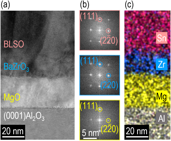
a Cross-sectional image of a transmission electron microscope clearly showing the BLSO film, the BaZrO3/MgO template bilayer, and the Al2O3 substrate. b Fast Fourier transformation images of selected areas indicating (111)-oriented epitaxial growth of the BLSO film and the BaZrO3 template bilayer. c Energy-dispersive X-ray spectroscopy data showing negligible intermixing of Sn (red), Zr (blue), Mg (yellow), and Al (white) atoms in the layers.
-
(6)
Energy-dispersive X-ray spectroscopy showed uniform distributions of Sn (red), Zr (blue), Mg (yellow), and Al (white) atoms over the entire area; this result indicated minimal atomic intermixing among the film, template bilayer, and substrate (Fig. 3c).
-
(7)
The atomic force microscopy image over a 2 × 2-μm2 area (Fig. S7) showed that the ~480-nm-thick films were smooth (0.8−1.7 nm in root-mean-square roughness).
-
(8)
We also considered Y-stabilized ZrO2 (YSZ), Gd-doped CeO2 (GDC), and ZnO epitaxial films as template layers (Table S2) since these films have been epitaxially grown on (0001)-oriented Al2O3 substrates34,35,36,37,38,39,40. We noted that the lattice mismatch between MgO and Al2O3 was smaller than −1.6% for 2:3 YSZ:Al2O3 for \([1\bar{1}0]\)YSZ || [100]Al2O3, 7.7% for [\(\bar{1}\bar{1}2\)]GDC || [100]Al2O3, and −15.4% for [110]ZnO || [210]Al2O3. More importantly, the lattice mismatch between BLSO and MgO was smaller than −11.9% for [\(100\)]BLSO || \([1\bar{1}0]\)YSZ, −19.5% for [\(0\bar{1}1\)]BLSO || \([\bar{1}\bar{1}2]\)GDC, and 9.5% for [\(1\bar{1}0\)]BLSO || [\(\bar{1}00\)]ZnO.

Excellent conducting properties of Ba1−xLaxSnO3 epitaxial films on Al2O3
Since the electrical properties of both BLSO epitaxial films and single crystals depend on the La concentration11,17, we systematically investigated this dependence for \({{\rm{BLSO}}}_{{{\rm{Al}}}_{2}{{\rm{O}}}_{3}}^{{\rm{BaZr}}{{\rm{O}}}_{3}/{\rm{MgO}}}\) with different La concentrations (5%, 10%, 15%, and 20%) and compared it with those of \({{\rm{BLSO}}}_{{\rm{SrTi}}{{\rm{O}}}_{3}}\) and \({{\rm{BLSO}}}_{{{\rm{Al}}}_{2}{{\rm{O}}}_{3}}\). Notably, the Ba atoms could be substituted by La atoms at least up to 20% in pulsed-laser-deposited BLSO films (Table S3)17. As already noted for the 5% concentration in Fig. 1, the BaZrO3/MgO template bilayer produced 1−2 orders of magnitude lower sheet resistances for the Ba0.9La0.1SnO3, Ba0.85La0.15SnO3, and Ba0.8La0.2SnO3 films than those for \({{\rm{BLSO}}}_{{{\rm{Al}}}_{2}{{\rm{O}}}_{3}}\) (Figs. S8 and S9). This optimal La concentration was consistent with 5−10% of La-doped17, Gd-doped19, Nb-doped20, and Ta-doped21 BaSnO3 films. As the \(5 \% -{{\rm{BLSO}}}_{{{\rm{Al}}}_{2}{{\rm{O}}}_{3}}^{{\rm{BaZr}}{{\rm{O}}}_{3}/{\rm{MgO}}}\) was studied as noted above, the template bilayer approach also enhanced the crystallinities of 10%, 15%, and 20% doped films (Figs. S10–S12).
As shown in Fig. 4a, the conductivities of the \({{\rm{BLSO}}}_{{{\rm{Al}}}_{2}{{\rm{O}}}_{3}}^{{\rm{BaZr}}{{\rm{O}}}_{3}/{\rm{MgO}}}\) and \({{\rm{BLSO}}}_{{\rm{SrTi}}{{\rm{O}}}_{3}}\) films decreased with increasing La concentration (e.g., 630 Ω−1 cm−1 for \(5 \% -{{\rm{BLSO}}}_{{{\rm{Al}}}_{2}{{\rm{O}}}_{3}}^{{\rm{BaZr}}{{\rm{O}}}_{3}/{\rm{MgO}}}\) and 35 Ω−1 cm−1 for \(20 \% -{{\rm{BLSO}}}_{{{\rm{Al}}}_{2}{{\rm{O}}}_{3}}^{{\rm{BaZr}}{{\rm{O}}}_{3}/{\rm{MgO}}}\)). The conductivity of \({{\rm{BLSO}}}_{{{\rm{Al}}}_{2}{{\rm{O}}}_{3}}\) was similar to the 0.1−1 Ω−1 cm−1 value for polycrystalline crystals11 and did not show any clear dependence on La concentration; this result indicated that electron scattering at the grain boundaries dominated the resistivity of the polycrystalline materials.

Decrease in a room temperature conductivity σ, b carrier density n, and c mobility μ with increasing La concentration. d Increase in the FWHM of (222)\({{\rm{BLSO}}}_{{{\rm{Al}}}_{2}{{\rm{O}}}_{3}}^{{\rm{BaZr}}{{\rm{O}}}_{3}/{\rm{MgO}}}\) with increasing La concentration. e Extent of crystallinity (smaller FWHM indicates more crystallinity) and conductivity (higher mobility indicates more conductivity) showing positive correlations. We also include data for the conductivity of \({{\rm{BLSO}}}_{{{\rm{Al}}}_{2}{{\rm{O}}}_{3}}\) (black triangles) in (a). For \({{\rm{BLSO}}}_{{{\rm{Al}}}_{2}{{\rm{O}}}_{3}}\), the conductivity shows no clear dependence on La concentration.
Next, we investigated the dependence of the carrier density and mobility on the La concentration. Considering carrier density first (Fig. 4b), its value decreased from 14.1 to 4.2 × 1020 cm−3 for both \({{\rm{BLSO}}}_{{{\rm{Al}}}_{2}{{\rm{O}}}_{3}}^{{\rm{BaZr}}{{\rm{O}}}_{3}/{\rm{MgO}}}\) and \({{\rm{BLSO}}}_{{\rm{SrTi}}{{\rm{O}}}_{3}}\) as the La concentration increased from 5% to 20%. As expected, the carrier densities of the \({{\rm{BLSO}}}_{{{\rm{Al}}}_{2}{{\rm{O}}}_{3}}^{{\rm{BaZr}}{{\rm{O}}}_{3}/{\rm{MgO}}}\) and \({{\rm{BLSO}}}_{{\rm{SrTi}}{{\rm{O}}}_{3}}\) epitaxial films were very similar. Moreover, the theoretical carrier density increased from 7.2 to 28.7 × 1020 cm−3 as the La concentration increased; this was calculated by assuming that all electrons generated by La3+ doping in a unit cell of Ba2+Sn4+O3 contributed to the electrical transport. Next, considering the carrier mobility (Fig. 4c), the mobility decreased from 2.8 (5% La) to 0.8 cm2 V−1 s−1 (20%) with increasing La doping. A similar decrease in carrier mobility occurred for \({{\rm{BLSO}}}_{{\rm{SrTi}}{{\rm{O}}}_{3}}\), i.e., 16.8 (5% La) to 3.4 cm2 V−1 s−1 (20%). The decrease in carrier density and mobility with increasing La concentration is well understood based on ionized impurity scattering, which is a universal process that occurs in all doped semiconductors13.
Since conductivity is proportional to the product of carrier density and mobility, the highest conductivity would be expected for the most crystalline films of the lowest La concentration. The evidence of poorer crystallinity with increasing La concentration was shown by the increasing FWHM of the XRD ω scans (Fig. 4d). In Fig. 4e, the conductivity of \({{\rm{BLSO}}}_{{{\rm{Al}}}_{2}{{\rm{O}}}_{3}}^{{\rm{BaZr}}{{\rm{O}}}_{3}/{\rm{MgO}}}\) increased as the FWHM decreased, indicating an affirmative correlation between conductivity and crystallinity.
High transmittance of Ba1−xLaxSnO3 epitaxial films on Al2O3
Figure 5a shows the relationship between the transmittance and La concentration for \({{\rm{BLSO}}}_{{{\rm{Al}}}_{2}{{\rm{O}}}_{3}}^{{\rm{BaZr}}{{\rm{O}}}_{3}/{\rm{MgO}}}\) in the wavelength range of 200−3300 nm, along with a comparison to the transmittance of \({5 \% -{\rm{BLSO}}}_{{\rm{SrTi}}{{\rm{O}}}_{3}}\). \(5 \% -{{\rm{BLSO}}}_{{{\rm{Al}}}_{2}{{\rm{O}}}_{3}}^{{\rm{BaZr}}{{\rm{O}}}_{3}/{\rm{MgO}}}\) demonstrates a high transmittance of ~82% over visible wavelengths of 400−1000 nm and was transparent even at ~300 nm. A clear “DGIST” logo was observed through both the Al2O3 substrate and our \(5 \% -{{\rm{BLSO}}}_{{{\rm{Al}}}_{2}{{\rm{O}}}_{3}}^{{\rm{BaZr}}{{\rm{O}}}_{3}/{\rm{MgO}}}\) film (top of Fig. 5a), indicating that our film was as transparent as the bare Al2O3 substrate. \({5 \% -{\rm{BLSO}}}_{{\rm{SrTi}}{{\rm{O}}}_{3}}\) exhibited a lower transmittance (~70%) in the visible region and had an abrupt suppression of transmittance below ~400 nm. Since Al2O3 has a much larger bandgap (~8.8 eV for corundum Al2O3)30 than the 3.2 eV of SrTiO3, it did not contribute to the ultraviolet absorption edge of \({5 \% -{\rm{BLSO}}}_{{{\rm{Al}}}_{2}{{\rm{O}}}_{3}}^{{\rm{BaZr}}{{\rm{O}}}_{3}/{\rm{MgO}}}\) [and \(5 \% -{{\rm{BLSO}}}_{{{\rm{Al}}}_{2}{{\rm{O}}}_{3}}\) (Fig. S13)]. This result indicated the importance of epitaxial films grown on wide-bandgap substrates to achieve high ultraviolet transmittance. From the abrupt suppression of ultraviolet transmittance near 300 nm, we estimated that the bandgap of Ba0.95La0.05SnO3 films was ~4.1 eV, similar to the bandgap of BLSO single crystals11. The transmittance was suppressed at infrared wavelengths (>1000 nm), and this suppression was attributed to the free electron response. In summary, \({5 \% -{\rm{BLSO}}}_{{{\rm{Al}}}_{2}{{\rm{O}}}_{3}}^{{\rm{BaZr}}{{\rm{O}}}_{3}/{\rm{MgO}}}\) was more transparent over a wider part of the ultraviolet‒visible spectrum than \({5 \% -{\rm{BLSO}}}_{{\rm{SrTi}}{{\rm{O}}}_{3}}\).

a Transmittance of \({{\rm{BLSO}}}_{{{\rm{Al}}}_{\boldsymbol{2}}{{\rm{O}}}_{\boldsymbol{3}}}^{{\rm{BaZr}}{{\rm{O}}}_{\boldsymbol{3}}/{\rm{MgO}}}\). All BLSO epitaxial films exhibited high transmittance (~82%) in the visible region. The fundamental absorption edges of \({{\rm{BLSO}}}_{{{\rm{Al}}}_{\boldsymbol{2}}{{\rm{O}}}_{\boldsymbol{3}}}^{{\rm{BaZr}}{{\rm{O}}}_{\boldsymbol{3}}/{\rm{MgO}}}\) (solid line) (at which the transmittance decreases sharply at ultraviolet wavelengths) are located at shorter wavelengths compared with the absorption edges of \({{\rm{BLSO}}}_{{\rm{SrTi}}{{\rm{O}}}_{\boldsymbol{3}}}\) (dashed line). Dotted lines indicate the transmittances of Al2O3 and SrTiO3 substrates. Oscillations can presumably be attributed to interference involving light reflected from the films and substrates of the ~480-nm-thick BLSO structures45. On the top of a, a clear “DGIST” logo is observed through both the Al2O3 substrate (left) and our \(5 \% -{{\rm{BLSO}}}_{{{\rm{Al}}}_{\boldsymbol{2}}{{\rm{O}}}_{\boldsymbol{3}}}^{{\rm{BaZr}}{{\rm{O}}}_{\boldsymbol{3}}/{\rm{MgO}}}\) film (right), indicating that our film is as transparent as the bare Al2O3 substrate. b Total electromagnetic shielding effectiveness (SE) of \({{\rm{BLSO}}}_{{{\rm{Al}}}_{\boldsymbol{2}}{{\rm{O}}}_{\boldsymbol{3}}}^{{\rm{BaZr}}{{\rm{O}}}_{\boldsymbol{3}}/{\rm{MgO}}}\). \(5 \% -{{\rm{BLSO}}}_{{{\rm{Al}}}_{\boldsymbol{2}}{{\rm{O}}}_{\boldsymbol{3}}}^{{\rm{BaZr}}{{\rm{O}}}_{\boldsymbol{3}}/{\rm{MgO}}}\) exhibits an SE of ~18.6 dB at 10 GHz.
The fundamental ultraviolet absorption edges for all \({{\rm{BLSO}}}_{{{\rm{Al}}}_{2}{{\rm{O}}}_{3}}^{{\rm{BaZr}}{{\rm{O}}}_{3}/{\rm{MgO}}}\) films were predominantly located near 300 nm. Upon closer observation, this edge, related to the bandgap, was weakly proportional to the carrier density (Figs. S14 and S15), which could be explained by the Burstein–Moss band-filling effect17. The donor level of n-type BLSO was ~46 meV below the conduction band18. The thermal energy (~25 meV) at room temperature spreads out the optical absorption from the donor level to the conduction band. Therefore, the ultraviolet‒visible transmittance was similar (~82%) because the transitions from the valence bands to the conduction bands primarily determine the bandgap of \({{\rm{BLSO}}}_{{{\rm{Al}}}_{2}{{\rm{O}}}_{3}}^{{\rm{BaZr}}{{\rm{O}}}_{3}/{\rm{MgO}}}\).
The infrared transmittance of \({{\rm{BLSO}}}_{{{\rm{Al}}}_{2}{{\rm{O}}}_{3}}^{{\rm{BaZr}}{{\rm{O}}}_{3}/{\rm{MgO}}}\) was sensitive to La concentration, in contrast to the marginal dependence of ultraviolet‒visible transmittance. The suppression of infrared transmittance was stronger in \({5 \% -{\rm{BLSO}}}_{{{\rm{Al}}}_{2}{{\rm{O}}}_{3}}^{{\rm{BaZr}}{{\rm{O}}}_{3}/{\rm{MgO}}}\) than in \({20 \% -{\rm{BLSO}}}_{{{\rm{Al}}}_{2}{{\rm{O}}}_{3}}^{{\rm{BaZr}}{{\rm{O}}}_{3}/{\rm{MgO}}}\). The Drude–Lorentz model assumes that the free carrier absorption coefficient is proportional to the carrier density41. Thus, the absorption coefficient of \({5 \% -{\rm{BLSO}}}_{{{\rm{Al}}}_{2}{{\rm{O}}}_{3}}^{{\rm{BaZr}}{{\rm{O}}}_{3}/{\rm{MgO}}}\) was larger than that of \({20 \% -{\rm{BLSO}}}_{{{\rm{Al}}}_{2}{{\rm{O}}}_{3}}^{{\rm{BaZr}}{{\rm{O}}}_{3}/{\rm{MgO}}}\) (Fig. S16) because the carrier density increased as the La concentration decreased (Fig. 4b). We observed a similar La concentration dependence of the infrared transmittance for \({{\rm{BLSO}}}_{{\rm{SrTi}}{{\rm{O}}}_{3}}\) (Fig. S17).
High electromagnetic shielding of the Ba1−xLaxSnO3 epitaxial films on Al2O3
The enhanced conductivity of \({5 \% -{\rm{BLSO}}}_{{{\rm{Al}}}_{2}{{\rm{O}}}_{3}}^{{\rm{BaZr}}{{\rm{O}}}_{3}/{\rm{MgO}}}\) led to increased electromagnetic shielding. Figure 5b shows the La concentration dependence of the shielding effectiveness (SE) of \({{\rm{BLSO}}}_{{{\rm{Al}}}_{2}{{\rm{O}}}_{3}}^{{\rm{BaZr}}{{\rm{O}}}_{3}/{\rm{MgO}}}\), measured via the coaxial transmittance line method over the X-band frequency range (8.5−12.5 GHz)32,33,42. The SE values increased as the La concentration decreased (e.g., ~18.6 dB at 10 GHz for Ba0.95La0.05SnO3 and ~12.6 dB for Ba0.8La0.2SnO3) due to increasing conductivity; this was consistent with Simon’s formula43. The high SE of \({5 \% -{\rm{BLSO}}}_{{{\rm{Al}}}_{2}{{\rm{O}}}_{3}}^{{\rm{BaZr}}{{\rm{O}}}_{3}/{\rm{MgO}}}\) was comparable with the SE values of the metal films, metal meshes, and two-dimensional materials; Table S4 provides comparisons of resistivity, SE, and visible transmittance among various electromagnetic shielding materials4,5,6,7,8,9,10,34,40,43. The SE (=SEA + SER) can be divided into SEA (shielding by absorption through \({{\rm{BLSO}}}_{{{\rm{Al}}}_{2}{{\rm{O}}}_{3}}^{{\rm{BaZr}}{{\rm{O}}}_{3}/{\rm{MgO}}}\)) and SER (shielding by reflection from the BLSO film). The SEA of ~14.1 dB at 10 GHz was greater than the SER of ~4.6 dB (Fig. S18); this result indicated that the electromagnetic shielding of BLSO was dominated by absorption.
Overall, \({{\rm{BLSO}}}_{{{\rm{Al}}}_{2}{{\rm{O}}}_{3}}^{{\rm{BaZr}}{{\rm{O}}}_{3}/{\rm{MgO}}}\) shows strong promise for electromagnetic shielding applications, which prevent radiation from damaging human health, malfunctioning sensitive electronic systems, and neutralizing military stealth technology. Our \({{\rm{BLSO}}}_{{{\rm{Al}}}_{2}{{\rm{O}}}_{3}}^{{\rm{BaZr}}{{\rm{O}}}_{3}/{\rm{MgO}}}\) films possess both high transparency and high stability, providing potential advantages over metal meshes, carbon-based meshes, or two-dimensional electromagnetic shielding materials4,5,6,7,8,9,10,34,40,43; these materials have one or more of the following challenges: conductivity loss arising from mesh structures, high corrosion, mechanical weakness, poor shapability, and difficulty achieving mass production. The combined high transparency and high stability of \({{\rm{BLSO}}}_{{{\rm{Al}}}_{2}{{\rm{O}}}_{3}}^{{\rm{BaZr}}{{\rm{O}}}_{3}/{\rm{MgO}}}\) shows potential for new applications that work in extreme environments, including invisible circuits, smart windows, and transparent solar cells32,33,42.
Conclusions
We used a BaZrO3/MgO template bilayer approach to create high-quality Ba0.95La0.05SnO3 epitaxial films on (0001)Al2O3 substrates and, in doing so, imparted single-crystalline level, transparent, conducting, electromagnetic shielding properties to the BLSO films. The epitaxial films exhibited a lower sheet resistance by three orders of magnitude compared with Ba0.95La0.05SnO3 films grown directly on Al2O3. Compared to higher La concentration levels, 5% produced the lowest sheet resistance since it produced the least scattering of the free electrons. The use of an Al2O3 substrate ensured high ultraviolet‒visible transmittance (~82%) of the BLSO films, which was seldom achieved when epitaxial BLSO films were grown on expensive SrTiO3. Our transparent, conducting, electromagnetic shielding BLSO films grown on Al2O3 are suited to applications in invisible circuits, smart windows, and transparent solar cells because of their low sheet resistance, high transmittance, high SE, chemical and mechanical stability, and simple large-area fabrication.
Materials and methods
Templated epitaxy of BLSO films
We used pulsed laser deposition to grow ~480-nm-thick BLSO films on (0001)-oriented Al2O3 with a BaZrO3/MgO template bilayer. To deposit the film and template bilayer, we ablated Ba1−xLaxSnO3 (x = 0.05, 0.1, 0.15, and 0.2), BaZrO3, and MgO pellets using an excimer laser (IPEX-760; LightMachinery Inc.) with a wavelength of 248 nm, intensity of 1.5 J cm–2, and repetition rate of 10 Hz. We heated the substrate to 750 °C using a lamp. For BLSO and BaZrO3 depositions, we maintained an oxygen partial pressure of 75 mTorr using a mass flow controller. However, we used 10 mTorr oxygen partial pressure for MgO growth because the MgO diffraction peaks in the XRD θ−2θ scan disappeared when the MgO films were deposited at 75 mTorr. For comparison, we deposited the BLSO films on (0001)Al2O3 without the template bilayer and we also deposited the epitaxial films on (001)SrTiO3.
Characterization of structural properties
We examined the structural properties using a four-circle high-resolution X-ray diffractometer (Empyrean; PANalytical) that emitted Cu radiation with a wavelength of 1.54 Å. We acquired cross-sectional images by using a transmission electron microscope (HF-3300; Hitachi), which was operated at 300 kV with a lattice resolution of ≥1 Å. Fast Fourier transformation was performed using Digital Micrograph software (Gatan Inc.). Energy-dispersive X-ray spectroscopy was used to study the microstructures and elemental distributions of the film and the template bilayer. An atomic force microscope (XE7; Park Systems) operating in tapping mode was used to obtain the surface images and roughness values. The scan area and rate were 2 × 2 μm2 and 0.6 Hz, respectively.
Measurement of the transparent conducting properties
To investigate the transport properties, we performed direct-current magnetron sputtering to deposit four Pt pads on film surfaces. Using a physical property measurement system (Quantum Design Inc.), we measured the resistances (<10 MΩ) under applied currents upon cooling and subsequent heating over the temperature range of 10−400 K. We calculated the sheet resistance through the multiplication of the measured resistance by the geometric factor (2.5) of the films44. To determine the carrier density and mobility, we obtained Hall measurements in a magnetic field that ranged from −4 to 4 T at 300 K. To directly measure transmittance, we examined films grown on double-sided polished substrates using the transmission mode of an ultraviolet‒visible near-infrared spectrophotometer in the wavelength range from 175 to 3300 nm (Cary 5000; Agilent Technologies).
Measurement of electromagnetic SE
We used a network analyzer (N5222A; Agilent Technologies) to measure SE in the two-coaxial, transmission line configuration. We grew films on double-sided polished (0001)Al2O3 substrates (area, 22.8 × 10.1 mm2; thickness, 2 mm). Each sample was positioned between two waveguides for measurement of the S parameters (S11 and S21) using an electromagnetic wave emitted by port 1. S11 was determined by detecting the reflected wave at port 1. S21 was acquired by detecting the wave transmitted (through the films and the Al2O3 substrate) at port 2. The total SE was calculated by summing the contributions of absorption (\({{\rm{SE}}}_{{\rm{A}}}=10\log \frac{1-{\left|{S}_{11}\right|}^{2}}{{\left|{S}_{21}\right|}^{2}}\)) and reflection (\({{\rm{SE}}}_{{\rm{R}}}=10\log \frac{1}{1-{\left|{S}_{11}\right|}^{2}}\))5,6. Because the SEA exceeded 10 dB, we disregarded the shielding by multiple reflections5.
Data availability
The data supporting the findings of this study are available from the corresponding author upon reasonable request.
References
Wilson, R., George, G. & Joseph, K. Materials for Potential EMI Shielding Applications (Elsevier, 2020).
Liu, J. et al. Hydrophobic, flexible, and lightweight MXene foams for high-performance electromagnetic-interference shielding. Adv. Mater. 29, 1702367 (2017).
Corredores, Y. et al. Adjustment of shielding effectiveness, optical transmission, and sheet resistance of conducting films deposited on glass substrates. IEEE Trans. Electromagn. Compat. 59, 1070–1078 (2017).
Yang, Y., Gupta, M. C., Dudley, K. L. & Lawrence, R. W. Novel carbon nanotube–polystyrene foam composites for electromagnetic interference shielding. Nano Lett. 5, 2131–2134 (2005).
Yuan, B., Yu, L., Sheng, L., An, K. & Zhao, X. Comparison of electromagnetic interference shielding properties between single-wall carbon nanotube and graphene sheet/polyaniline composites. J. Phys. D-Appl. Phys. 45, 235108 (2012).
Liang, X. et al. Room-temperature nanowelding of a silver nanowire network triggered by hydrogen chloride vapor for flexible transparent conductive films. ACS Appl. Mater. Interfaces 9, 40857–40867 (2017).
Wan, S. et al. Sequentially bridged graphene sheets with high strength, toughness, and electrical conductivity. Proc. Natl Acad. Sci. USA 115, 5359–5364 (2018).
Li, Y. et al. Scalable manufacturing of flexible, durable Ti3C2Tx MXene/Polyvinylidene fluoride film for multifunctional electromagnetic interference shielding and electro/photo-thermal conversion applications. Composites Pt. B-Eng. 217, 108902 (2021).
Zhou, B. et al. Aramid nanofiber-derived carbon aerogel film with skin-core structure for high electromagnetic interference shielding and solar–thermal conversion. Carbon 184, 562–570 (2021).
Liang, L. et al. High-efficiency electromagnetic interference shielding capability of magnetic Ti3C2Tx MXene/ CNT composite film. J. Mater. Chem. A 9, 24560–24570 (2021).
Luo, X. et al. High carrier mobility in transparent Ba1−xLaxSnO3 crystals with a wide band gap. Appl. Phys. Lett. 100, 172112 (2012).
Kim, H. J. et al. Physical properties of transparent perovskite oxides (Ba,La)SnO3 with high electrical mobility at room temperature. Phys. Rev. B 86, 165205 (2012).
Ellmer, K. Past achievements and future challenges in the development of optically transparent electrodes. Nat. Photon. 6, 809–817 (2012).
Yu, X., Marks, T. J. & Facchetti, A. Metal oxides for optoelectronic applications. Nat. Mater. 15, 383–396 (2016).
Morales-Masis, M., De Wolf, S., Woods-Robinson, R., Ager, J. W. & Ballif, C. Transparent electrodes for efficient optoelectronics. Adv. Electron. Mater. 3, 1600529 (2017).
Kim, H. J. et al. High mobility in a stable transparent perovskite oxide. Appl. Phys. Express 5, 061102 (2012).
Liu, Q. et al. Composition dependent metal-semiconductor transition in transparent and conductive La-doped BaSnO3 epitaxial films. Appl. Phys. Lett. 101, 241901 (2012).
Liu, H.-R., Yang, J.-H., Xiang, H. J., Gong, X. G. & Wei, S.-H. Origin of the superior conductivity of perovskite Ba(Sr)SnO3. Appl. Phys. Lett. 102, 112109 (2013).
Liu, Q. et al. Optical and transport properties of Gd doped BaSnO3 epitaxial films. J. Alloy. Compd. 647, 959–964 (2015).
Li, B., Liu, Q., Zhang, Y., Liu, Z. & Geng, L. Highly conductive Nb doped BaSnO3 thin films on MgO substrates by pulsed laser deposition. J. Alloy. Compd. 680, 343–349 (2016).
Liu, Q. et al. Transparent and conductive Ta doped BaSnO3 films epitaxially grown on MgO substrate. J. Alloy. Compd. 684, 125–131 (2016).
Shin, S. S. et al. Colloidally prepared La-doped BaSnO3 electrodes for efficient, photostable perovskite solar cells. Science 356, 167–171 (2017).
Prakash, A. et al. Wide bandgap BaSnO3 films with room temperature conductivity exceeding 104 S cm−1. Nat. Commun. 8, 15167 (2017).
Sanchela, A. V. et al. Large thickness dependence of the carrier mobility in a transparent oxide semiconductor, La-doped BaSnO3. Appl. Phys. Lett. 112, 232102 (2018).
Xing, S. M. et al. Optoelectronic properties and interband transition of La-doped BaSnO3 transparent conducting films determined by variable temperature spectral transmittance. J. Appl. Phys. 117, 103107 (2015).
Tiwari, A. & Wong, M. S. Substrate temperature effect on structure and properties of sputtered polycrystalline transparent conducting oxide films of La-doped BaSnO3. Thin Solid Films 715, 138427 (2020).
Zala, D., Joshi, U. S. & Ray, A. Structural and optical analysis of perovskite La-doped BaSnO3 bulk and thin films. Mater. Today: Proc. 67, 927–930 (2022).
Du, J., Gnanarajan, S. & Bendavid, A. Characterization of MgO substrates for growth of epitaxial YBCO thin films. Supercond. Sci. Technol. 18, 1035–1041 (2005).
Schroeder, J. L., Ingason, A. S., Rosén, J. & Birch, J. Beware of poor-quality MgO substrates: a study of MgO substrate quality and its effect on thin film quality. J. Cryst. Growth 420, 22–31 (2015).
Filatova, E. O. & Konashuk, A. S. Interpretation of the changing the band gap of Al2O3 depending on its crystalline form: connection with different local symmetries. J. Phys. Chem. C 119, 20755–20761 (2015).
Ohring, M. Materials Science of Thin Films (Academic Press, San Diego, CA, USA, 2002).
Kim, D. & Lee, S. Stable Sn-doped In2O3 films coated on Al2O3 for infrared transparent and electromagnetic shielding conductors. Appl. Surf. Sci. 604, 154149 (2022).
Ha, Y. & Lee, S. Stable correlated 4d2 SrMoO3 films epitaxially coated on Al2O3 for electromagnetic shielding and transparent conductors. Adv. Mater. Interface 9, 2200893 (2022).
Stampe, P. A., Bullock, M., Tucker, W. P. & Kennedy, R. J. Growth of MgO thin films on M-, A-, C- and R-plane sapphire by laser ablation. J. Phys. D-Appl. Phys. 32, 1778–1787 (1999).
Kawasaki, M. et al. Excitonic ultraviolet laser emission at room temperature from naturally made cavity in ZnO nanocrystal thin films. Mater. Sci. Eng. B-Adv. Funct. Solid-state Mater. 56, 239–245 (1998).
Kato, H., Miyamoto, K., Sano, M. & Yao, T. Polarity control of ZnO on sapphire by varying the MgO buffer layer thickness. Appl. Phys. Lett. 84, 4562–4564 (2004).
Pergolesi, D., Fronzi, M., Fabbri, E., Tebano, A. & Traversa, E. Growth mechanisms of ceria- and zirconia-based epitaxial thin films and hetero-structures grown by pulsed laser deposition. Mater. Renew. Sustain. Energy 2, 6 (2013).
Jiang, J., Hu, X., Shen, W., Ni, C. & Hertz, J. L. Improved ionic conductivity in strained yttria-stabilized zirconia thin films. Appl. Phys. Lett. 102, 143901 (2013).
Krishnaprasad, P. S., Antony, A., Rojas, F. & Jayaraj, M. K. Domain matched epitaxial growth of (111) Ba0.5Sr0.5TiO3 thin films on (0001)Al2O3 with ZnO buffer layer. J. Appl. Phys. 117, 124102 (2015).
Rasic, D., Sachan, R., Temizer, N. K., Prater, J. & Narayan, J. Oxygen effect on the properties of epitaxial (110) La0.7Sr0.3MnO3 by defect engineering. ACS Appl. Mater. Interfaces 10, 21001–21008 (2018).
Fox, M. Optical Properties of Solids (Oxford University Press Inc., New York, USA, 2010).
Ha, Y. et al. Infrared transparent and electromagnetic shielding correlated metals via lattice-orbital-charge coupling. Nano Lett. 22, 6573–6579 (2022).
Shahzad, F. et al. Electromagnetic interference shielding with 2D transition metal carbides (MXenes). Science 353, 1137–1140 (2016).
Sze, S. M. & Ng, K. K. Physics of Semiconductor Devices (John Wiley & Sons. Inc., Hoboken, JN, USA, 2007).
Zhyrair, G. et al. Determination of the complete set of optical parameters of micron-sized polycrystalline CH3NH3PbI3−xClx films from the oscillating transmittance and reflectance spectra. Mater. Res. Express 7, 016408 (2020).
Acknowledgements
This work was supported by national R&D programs of the National Research Foundation of Korea funded by the Ministry of Science and ICT (project nos. NRF-2021M3F3A2A03015439, NRF-2021R1C1C1005042, and NRF-2018R1A5A1025511). We also acknowledge partial support from national R&D programs of the National Research Foundation of Korea funded by the Ministry of Education (project no. NRF-2021R1A6A3A13043948) and the DGIST R&D program of the Ministry of Science and ICT of Korea (project nos. 22-HRHR+-05, 22-CoE-NT-02, and 22-SENS-1). S.L. and J.L.M.-D. would like to thank Trinity College at Cambridge for partial support. J.L.M.-D. would like to thank the EU-H2020-ERC-ADG # 882929 grant, EROS, and the Royal Academy of Engineering CIET1819_24 for partial support.
Author information
Authors and Affiliations
Contributions
Y.H., J.J., and S.H. conducted the experiments and wrote the manuscript under the supervision of S.L. Y.H. and J.J. equally contributed to this work. J.L.M.-D. contributed to the science and manuscript writing. All authors reviewed the paper.
Corresponding author
Ethics declarations
Conflict of interest
The authors declare no competing interests.
Additional information
Publisher’s note Springer Nature remains neutral with regard to jurisdictional claims in published maps and institutional affiliations.
Supplementary information
Rights and permissions
Open Access This article is licensed under a Creative Commons Attribution 4.0 International License, which permits use, sharing, adaptation, distribution and reproduction in any medium or format, as long as you give appropriate credit to the original author(s) and the source, provide a link to the Creative Commons license, and indicate if changes were made. The images or other third party material in this article are included in the article’s Creative Commons license, unless indicated otherwise in a credit line to the material. If material is not included in the article’s Creative Commons license and your intended use is not permitted by statutory regulation or exceeds the permitted use, you will need to obtain permission directly from the copyright holder. To view a copy of this license, visit http://creativecommons.org/licenses/by/4.0/.
About this article

Cite this article
Ha, Y., Jeon, J., Hwang, S. et al. BaZrO3/MgO-templated epitaxy showing a conductivity increase of three orders of magnitude for the Ba0.95La0.05SnO3 films on Al2O3 substrates, with very high transparency and X-band electromagnetic shielding. NPG Asia Mater 15, 63 (2023). https://doi.org/10.1038/s41427-023-00512-w
Received:
Revised:
Accepted:
Published:
DOI: https://doi.org/10.1038/s41427-023-00512-w
