
Abstract
Fast flexible electronics operating at radio frequencies (>1 GHz) are more attractive than traditional flexible electronics because of their versatile capabilities, dramatic power savings when operating at reduced speed and broader spectrum of applications. Transferrable single-crystalline Si nanomembranes (SiNMs) are preferred to other materials for flexible electronics owing to their unique advantages. Further improvement of Si-based device speed implies significant technical and economic advantages. While the mobility of bulk Si can be enhanced using strain techniques, implementing these techniques into transferrable single-crystalline SiNMs has been challenging and not demonstrated. The past approach presents severe challenges to achieve effective doping and desired material topology. Here we demonstrate the combination of strained- NM-compatible doping techniques with self-sustained-strain sharing by applying a strain-sharing scheme between Si and SiGe multiple epitaxial layers, to create strained print-transferrable SiNMs. We demonstrate a new speed record of Si-based flexible electronics without using aggressively scaled critical device dimensions.
Introduction
Flexible electronics have been mainly addressing electronic applications operating at low or moderate speed1,2,3. For these applications, form factors such as bendability and large area are of more importance than speed. Organic semiconductors4,5 and amorphous6 or polycrystalline Si7, which can be processed at relatively low temperature and with low cost, often suffice to address them. On the other hand, there is a wider spectrum of electronics applications where higher speed and mechanical flexibility are simultaneously needed, such as high-speed and wireless communications, remote sensing and airborne/space surveillance8. We entitle the special category of such flexible electronics as fast flexible electronics. A number of applications even require the operating speed (frequency) be beyond 1 GHz and hence these applications can be further termed as radio frequency (RF) flexible electronics. Fast flexible electronics provide superior performance and application advantages. As is known, high-speed devices consume much less power if they are operated at a reduced speed9,10,11,25, which dramatically benefits battery powered devices. Wirelessly connected devices enabled only by high operation speed/frequency are more convenient to use than wired devices1 and a high-frequency wireless system is also generally more compact than a low-frequency one.
Transferrable mono-crystalline Si nanomembranes (NMs) are suitable for active material of fast flexible electronics when comparing with any other materials for flexible electronics owing to their material uniformity12, mechanical flexibility13 and durability14, electrical properties equivalent to their bulk counterparts15, easy handling16,17,18 and processing and low cost. Si has modest mobility values in comparison to most III–V and other materials19,20, but can be easily down scaled for performance improvement. As large critical device dimensions are generally preferred for flexible-electronics applications where cost and large area are often of the most concern, improving device speed using approaches other than dimension downscaling is preferred. Among them, strain engineering is one of the most effective ones21,22. In contrast to bulk Si, where strain in the active device layer can be easily sustained/held by a rigid substrate23, in transferrable Si nanomembranes strain needs to be self-sustained. Here we describe a combined strain compatible effective doping and strain engineering approach that is especially suited for transferrable Si NMs. Strain compatible device fabrication techniques then lead us to desired higher device speed on flexible substrates.
Results
Figure 1a illustrates the previously developed21,24 strain sharing techniques used to create self-sustained strain in Si NMs. First, 80 nm of undoped Si0.795Ge0.205 is epitaxially grown on silicon-on-insulator (SOI) with a 48 nm Si template layer. A nearly symmetrical trilayer structure (Si/SiGe/Si) is formed by growing 46 nm of undoped Si on top of the SiGe. Because of the lattice mismatch between Si and SiGe, the SiGe layer in the trilayer structure is compressively strained to the Si in-plane lattice constant (mismatch strain, εm = −0.77% for Si0.795Ge0.205). The trilayer NM is released by selective removal of the SiO2 (BOX) layer of the SOI. During the release, strain sharing occurs between the SiGe and Si layers; some of the compressive strain in the SiGe layer transfers as tensile strain to the outer Si layers. It is important to have a balanced trilayer structure (top and bottom layers approximately equal thickness) to prevent the heterostructure from curling during release from the handling substrate26. Of more importance, the tensile strain in Si layers is self-sustained by a balance of forces between the Si and SiGe layers in the freestanding trilayer NM21,24.

Strain sharing using Si/SiGe/Si epitaxial trilayer structure.
(a), i, Atomic lattice schematic diagram showing the strain sharing principle. Optical images show the strained NM during release and after finishing release. ii, Process flow to implement the strain sharing principle. (b), i, Critical and metastable thicknesses of SiGe that can be coherently grown on Si. ii, Si strain as a function of Ge fraction in SiGe used to guide the design and epitaxial growth of Si/SiGe/Si trilayer. (c), X-ray diffraction measurement verifying strain sharing. i, On-axis line scan around the (004) reflection before and after release of the trilayer NM. ii, Off-axis reciprocal-space map (RSM) around the (044) reflection for the as-grown trilayer structure.
The amount of strain transferred to the Si layers is determined by the Si/SiGe thickness ratio and Ge composition of the alloy layer, which controls the mismatch strain (εm) in the trilayer24. The thickness ratio determines the fractional amount of the mismatch strain in the SiGe alloy that is transferred to the Si layers. The magnitude of strain sharing between the layers increases with increasing SiGe thickness and decreasing Si thickness. The thickness of the SiGe, however, must be kept below the kinetic critical thickness for dislocation formation (Figure 1b)27 because in the as-grown state, the SiGe layer accommodates all the strain in the trilayer. Note that the kinetic critical thickness is different from (i.e., larger than) the thermodynamic critical thickness, because of kinetic barriers to dislocation formation. As the growth temperature is lowered the kinetic critical thickness increases. Thinning the Si in SOI mentioned above allows maximum strain sharing. Figure 1b shows the expected strain transfer to the Si layers as a function of Ge composition in the alloy layer and total Si layer thickness (tSi = thickness of top + bottom layers), assuming the alloy layer thickness is equal to the kinetic critical thickness for growth at 550°C. From knowledge of the layer thicknesses and Ge composition of the initial heterostructure, we expect ~0.35% biaxial tensile strain in the Si layers after strain sharing. Mobility enhancement is expected from the tensilely strained Si28.
To demonstrate the effectiveness of the self-sustained straining approach, Figure 1c shows an x-ray diffraction (XRD) off-axis reciprocal-space map (RSM) around the (044) reflection for the as-grown trilayer structure. The RSM indicates that the SiGe layer is strained to the Si lattice constant; the Si and SiGe peaks lie along the same vertical line. This result confirms that there is no plastic relaxation of the mismatch strain in the alloy before release of the trilayer (SiGe layer thickness is below kinetic critical thickness for dislocation formation). Figure 1c also illustrates the strain sharing results in the Si/SiGe/Si layer (an undoped sample is shown). On-axis XRD lines scans around the (004) reflection allow us to measure the out-of-plane lattice constant change that occurs during strain sharing. In the as-grown state the SiGe layer is compressively strained to the Si lattice constant; an in-plane compressive strain translates to an out-of-plane expansion (smaller Bragg angle). After release, the SiGe becomes less compressively strained and the Si layers become tensile strained. The expansion in the in-plane lattice constant leads to a reduction in the out-of-plane lattice constant of both layers. Both the SiGe and Si peaks shift to higher Bragg angles (+0.1 degree), indicating that elastic strain sharing occurs between SiGe and Si after release; the relaxation of compressive strain in the SiGe layer is equal to the tensile strain transferred to the Si layers. The strain in the trilayer NM is now self sustained in the released and freestanding NMs.
To realize high device speed and RF operation of devices, the NMs must be doped. The above discussion and all prior work that uses self-sustained strain relate to undoped NMs. When we attempted to dope the strained trilayer NM prior to release, using the doping approach that has been successfully applied to unstrained Si NMs29,30, the strained NM curled upon release and became very rough. Figure 2a briefly illustrates the application of the NM pre-release selective ion implantation doping approach, but being applied to the strained trilayer NM. A detailed doping process flow for unstrained Si NMs is shown in Figure S1. Figure 2b shows a 3D microscopic image of a doped and annealed trilayer NM after release from the handling substrate. As can be seen, the topology of the released trilayer NMs becomes unsuitable for further processing, such as transfer and patterning. We believe that the Si/SiGe/Si epilayer structure has been damaged through atomic mixing and crystalline defects created by the implanted ions. The subsequent annealing procedure intended for recrystallization failed to restore the ion implanted damaged layers and interfaces back to their original order. Instead, significant and unbalanced stress was built in the NM after performing the doping processes, which caused severe curling of the released NMs.

Doping of strain shared Si/SiGe/Si trilayer nanomembrane.
(a), Ion implantation and anneal processes are applied to as-grown Si/SiGe/Si trilayer. (b), i, Schematic of patterned strained NM for RF device fabrication. ii, 3D microscopic images of released strained trilayer, showing the un-flat topology. Note that the undoped region of the trilayer NM stays flat. (c), Doping of strained trilayer structure. i, Unstrained Si NM is ion implanted and annealed. ii, Si NM is thinned down. iii, SiGe and Si epi growth on thinned Si NM to form symmetric trilayer. iv, Release of Si/SiGe/Si trilayer. (d), Images of doped strained NM at different processing stages. i. Before release. ii. After finishing undercut, sitting on Si handling substrate. iii, After being transferred to a plastic substrate. (e), X-ray diffraction of as-grown ion-implanted trilayer NM. i. Off-axis reciprocal-space map (RSM) around the (044) reflection. ii. On-axis line scans around the (004) reflection comparing the doped and undoped as-grown trilayer NMs.
To realize effective doping while maintaining a flat topology of the flexible, strain-shared trilayer NM for fabrication of RF devices, we designed an alternative approach to strain-compatible effective doping processes (Figure 2c). Instead of applying the ion implantation and anneal processes directly on a trilayer NM, we first applied them to an unstrained Si layer on SOI. Typically, low-energy phosphorus ion implantation is used to heavily dope the top portion of a Si template layer, leaving the bottom portion barely damaged by the implanted ions. An annealing process follows to recrystallize the damage and simultaneously drive the implanted dopants to diffuse until they reach the bottom surface of the template layer, generating a high-level and nearly uniform doping profile across the entire Si template layer. Leaving the bottom portion of the template layer undamaged during implantation is critical, as the bottom portion serves as the seed layer for recrystallization of the entire layer during the annealing process. Detail of ion implantation conditions and results can be found in the Method Section and Figure S2. After finishing these processes, very low sheet resistance is obtained, which is needed to achieve high-frequency device operation (see the Method Section). For unstrained-device fabrication, used as reference devices in this work, the selectively doped Si template layer is ready for release and transfer to a flexible substrate.
To realize selectively doped trilayer Si NMs for RF device fabrication, the selectively doped unstrained Si template layer was thinned down followed by epitaxial growth of SiGe and Si layers as performed in the undoped trilayer NM case. Figure 2(d) shows images of trilayer NMs (in the form of strips) at the different stages of processing. The doped regions for the source/drain/source, with 1.5 μm gaps between them (a two-gate finger device), are clearly identifiable. It is noted that after finishing the growth, only the bottom Si layer is heavily and selectively doped, with little dopants diffusing back to the SiGe or to the top Si layers. The doping and thinning down procedures have some effect on the crystallinity of the as-grown Si/SiGe/Si trilayers (as indicated by a general broadening of the diffraction peaks in Figure 2e(ii)). The SiGe layer, however, is still strained to the Si lattice constant so strain sharing is expected to occur as predicted upon release of these trilayers (εSi = 0.34% ± 0.01%). With this amount of biaxial tensile strain in Si, we can expect a ~47% increase in the electron mobility28.
Figure 3a provides the illustration of the device (field effect thin-film transistor, TFT) fabrication procedures using the transferred trilayer NM, which is bonded to a polyethylene terephthalate (PET) substrate. Using a flip transfer procedure, the selectively doped source and drain regions on the bottom Si layer of the trilayer NM becomes the top surface. Following the procedures described previously31, the device fabrication is finished. Figures 3b and 3c show the cross section, dimensions and optical image of a finished device on a PET substrate. Figures 3d and 3e show the reference device fabrication and information on the unstrained Si NM. The gate length and channel length, which are identically applied to both the strained and the unstrained NM, are 2.5 and 1.5 μm, respectively.

Device fabrication on released strained Si/SiGe/Si NMs and characterizations.
(a), Process flow for device fabrication. i, Released strained NM sitting on handling substrate. ii–iii, NM is flip transferred to a PET substrate. iv, Gate stack formation using lift-off techniques. v, Source/drain and a interconnect spelling-metallization. (b), Cross sectional illustration of strained-NM device dimensions. (c), Optical image of a fabricated strained device. (d), Cross sectional illustration of unstrained device dimensions. (e), Optical image of a fabricated unstrained device. For both strained and unstrained devices, the gate lengths (Lg = Lch+Lsg+Ldg) is 2.5 μm and gate width is 40 μm. Having a gate overlap distance with source/drain regions (Lsg and Ldg) of 0.5 μm, the effective channel lengths (Lch) are 1.5 μm. (f), Device DC and RF response characteristics of unstrained and strained devices. i, Transfer curves and calculated transconductance (gm) curves of unstrained and strained devices (Vds = 500 mV). ii, gm is plotted as a function of drain current. Point A indicates the peak gm where peak fT/fmax values were measured. Point B is where 3.5 GHz fmax can be obtained. The drain current at point B is roughly two orders lower than that at point A. iii, Current gain (H21) and power gain (Gmax) as a function of frequency of unstrained and strained devices (Vg = 4 V, Vds = 5 V). iv and v, fT and fmax of strained devices as a function of gate bias under fixed drain bias (Vds = 5 V) and that as a function of drain bias under fixed gate bias (Vg = 4 V), respectively.
Figure 3f(i) shows the transfer curve and calculated transconductance (gm) versus gate voltage (Vg) of a strained-channel TFT along with the results measured from the unstrained-channel TFT for comparison. The highest gm values for the strained and the unstrained TFTs are 386 μS and 262 μS, respectively. Because the dimensions of the two devices are identical, the 47.3% enhancement of the peak gm values in the strained TFT is mainly ascribed to mobility enhancement, which is caused by the introduction of the tensile strain in the Si channel of the trilayer. The gm and mobility enhancement ratios are consistent with the expected values28. Figure 3f(ii) plots gm versus drain current. The roughly linear trend of gm as a function of logarithmic drain current is consistent with devices made on rigid substrates9,10,11. Figure 3f(iii) shows the measured current gain (H21) and power gain (Gmax) of the strained TFT, indicating that the cut-off frequency (fT) is 5.1 GHz and the maximum oscillation frequency (fmax) is 15.1 GHz. For RF applications (analog circuits), power gain is more significant than current gain, which is typically used for evaluating switching speed of (digital/logic) devices. As a result, fmax is considered a better indicator of the device's speed than fT. The fmax value sets a new speed record for Si-based TFTs fabricated on plastic substrates, even though critical dimensions of the strained channel are larger than the previously reported devices30 and a relatively thick gate dielectric (120 nm) is used. Considering biomedical wireless devices typically operating at 400 MHz32, for which both the strained-channel transistor (this work, on plastic) and poly-Si transistors (on glass) having a fmax of 3.5 GHz33 can be used, the strained transistor consumes roughly two orders less power than the poly-Si transistor, as indicated by points A and B in Figure 3f(ii). As a comparison, the unstrained reference TFT with identical dimensions has fT and fmax of 3.3 GHz and 10.3 GHz, respectively. The mobility enhancement (47.3%) is directly reflected in the device's speed enhancement: 54.5% for fT and 46.6% for fmax. Following the typical scaling law of field effect transistors, if a smaller device feature is applied to the strained-channel devices by using a previously demonstrated alignment scheme30, about 6 GHz fT and 18 GHz fmax can be expected. Figures 3f(iv–v) show the gate bias dependence under fixed drain bias and drain bias dependence under fixed gate bias of the frequency response characteristics of the strained-channel TFT, respectively. Overall, relatively low bias voltages and thus low power consumptions are needed to operate these high-speed flexible transistors, a significant advantage of the single-crystal NM based TFTs over the polycrystalline Si-based TFTs34, where much higher operation voltages are generally needed.
Figure 4 shows the mobility and RF characteristics of the strained and the unstrained transistors under bending situations along with the bending test setup and an optical image of a bent array on a PET substrate. Besides the effective mobility enhancement of 47.3% without applying any external strain, the mobility in both the strained and the unstrained transistor channels was further enhanced, 20% and 14.8%, respectively, by applying external uniaxial strain of 1.08% (measured from bending curvature). A mobility enhancement (13%) was also observed from the strained channel under a uniaxial externally applied compressive strain of −0.215%, indicating the possibility to create a complementary strain-shared structure: SiGe/Si/SiGe for higher-performance flexible transistors, where SiGe serves as the device channel. The measured mobility variation trends are consistent with that of strained bulk Si28. The frequency variation trend as a function of tensile strain (impossible to measure frequency response under concave bending due to large RF probe size) is consistent with that of the mobility. It is noted that the transistors remain intact and operational under high-strain conditions; a convex radius of curvature of 15.5 mm translates into an external strain of 1.08%.

Device characteristics under bending.
(a), Bending setup for RF measurements. (b), A bent device array on a bending fixture. (c), Calculated mobility values from measured transconductance as a function of bending induced strain for both unstrained and strained devices. (d), fT and fmax of both unstrained and strained devices as a function of bending induced external strain.
Discussion
In summary, we have demonstrated a simple and viable approach to realizing strained-mono-crystalline-Si RF transistors on flexible plastic substrates. This technique has great potential in low-power and high-speed flexible-electronics applications and could be used to replace a number of rigid counterparts for use in mechanically bendable and non-planar conformal surfaces where rigid devices cannot be easily used. One can foresee as a consequence manufacturable large-area applications of such flexible high-speed thin-film transistor technology.
Methods
Doping of unstrained Si nanomembrane
Effective doping of the SiNM is needed to reduce contact resistance in source and drain regions of RF transistors. Commercially available SOI (Soitec USA, 2 Centennial Drive, Peabody, MA 01960, USA) with 200 nm Si (001) template and 145 nm buried oxide (BOX) layers is used as the starting material. The Si (001) template is lightly doped with boron. Phosphorus ion implantation is used on the SOI substrate with a dose of 2 × 1015 cm−2 and an energy of 20 keV. Following the ion implantation, the sample is annealed in a high-temperature furnace at 950°C for 30 mins in N2 ambient to re-crystallize the Si template and activate the dopants. TEM cross section images of Si NMs (unstrained) before and after anneal are shown in Figure S1. The simulated and characterized doping profiles using secondary ion mass sepectroscopy (SIMS) before and after anneal are shown in Figure S2.
Thinning down Si nanomembrane
After the ion implantation, the Si template is treated in an RIE chamber (Unaxis 790, 30 W) with SF6/O2 for 40 sec. A dry thermal oxidation at 1050°C for 10 min is applied to the sample to further reduce the Si template to the desired thickness in the Si/SiGe/Si tri-layer structure. The final thickness of the Si template is 48 nm, as verified by XRD measurement.
Epitaxial growth of SiGe/Si layers
Si/SiGe/Si trilayer NM fabrication starts with molecular beam epitaxy (MBE) growth of thin SiGe alloy films on SOI(001) substrates with a ~48 nm top Si template layer and 150 nm buried oxide (BOX) layer. Our standard chemical cleaning procedure before growth on Si is as follows: [1] 20 sec in 10% HF, [2] 10 min in Piranha clean (~80°C H2SO4 + H2O2 solution), [3] 15 min in standard clean 1 [SC1] (~80°C H2O + NH4OH + H2O2 solution) and [4] 20 sec in 10% HF (with a 5-min DI water rinse between each step) before putting the sample directly into the high-vacuum growth chamber. We resistively heat the substrate to 475°C during pseudomorphic growth of the alloy and used a growth rate ~3 nm/min. θ/2θ lines scans around the (004) reflection (Figure 1c and 2e) were fit to simulations to extract the Ge composition of the SiGe layer and each of the layer thicknesses before release from the initial growth substrate: 46 nm Si/80 nm Si0.795Ge0.205/48 nm Si. In the as-grown heterostructure, the main peak at lower Bragg angles is from the SiGe layer and the broad peak modulated by the thickness fringes is from the two Si layers.
Strain calculation of Si in Si/SiGe/Si
The Ge composition will determine the mismatch strain and the thickness ratio controls the fractional amount of that mismatch strain that is transferred to the Si layers. The strain transferred to the Si layers is:

where Mi is the biaxial modulus and tiis the thickness of the respective layers. The mismatch strain, εm, is the amount of strain in the SiGe before release from the handling substrate.

Device fabrication
After the trilayer growth (for the strained-channel device) and ion implantation (for the unstrained-channel reference device), optical photolithography is used to pattern both types of the active layers into 40 μm wide strips, with 10 μm gaps between them etched using reactive ion etching (RIE). The photoresist on top is removed in acetone and the strips are released in a 4:1 diluted HF (49% HF) solution in which the BOX layer is selectively etched away. The strips fall onto the Si substrate and, during release, the trilayer Si/SiGe/Si structure shares strain elastically, leaving the top and bottom Si layers tensilely strained. Photoresist SU8-2002 (Microchem Corp.) is spun on the PET host substrate and the free-standing, elastically relaxed strips are transferred top side down onto the SU8 layer. To create better adhesion between the strips and SU8 layer, the Si substrate on which the strips had come to rest after release is gently pressed and then peeled off. The PET substrate is cured from the back side under UV light and baked at 105°C for 5 min. After this step, the strips are firmly attached to the PET substrate and ready for the subsequent processing. The color difference between doped source/drain regions and channel regions helps alignment of gate patterns. To make gate dielectric and gate metal contacts, 120 nm thick SiO, 20 nm thick Ti and 150 nm Au are evaporated on the channel areas defined by optical photolithography. The source/drain metal consisting of 20 nm Ti and 300 nm Au is formed on both types of the active layers by optical photolithography and liftoff.
DC and RF characterizations of devices
DC characteristics were measured with an Agilent 4155 semiconductor parameter analyzer in a dark environment. For RF characteristics, Scattering (S) parameter measurement was taken using an Agilent E8364A network analyzer. The “open” and “short” features were used for a de-embedding procedure to obtain the intrinsic RF characteristics of device. The de-embedding procedure follows the equation;

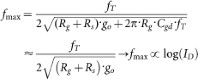
The effects of contact resistance fmax can be seen in the following equations:

where gm is transconductance, Cgd and Cgs are gate-drain and gate-to-source capacitance, respectively. go is output conductance. Rg and Rs are gate resistance and source resistance, respectively.
Power savings when operating a device at reduced speed
The relationship between power consumption (estimated only based on drain current, which is conservative) and fmax can be estimated by the following equations11:
-
Equation for calculating transconductance;

-
Equation for calculating drain current;

-
log(ID) is proportional to gm as follows;

-
Therefore the relationship between gm and RF response is as follows;


By plotting gm versus  , power consumption at lower fmax can be estimated.
References
Kim, D.-H. et al. Epidermal Electronics. Science 333, 838–843 (2011).
Kim, D.-H. et al. Materials and noncoplanar mesh designs for integrated circuits with linear elastic responses to extreme mechanical deformations. Proc. Natl Acad. Sci. USA 105, 18675–18680 (2008).
Ahn, J.-H. et al. Bendable integrated circuits on plastic substrates by use of printed ribbons of single-crystalline silicon. Appl. Phys. Lett. 90, 213501 (2007).
Forrest, S. R. The path to ubiquitous and low-cost organic electronic appliances on plastic. Nature 428, 911–918 (2004).
Gelinck, G. H. et al. Flexible active-matrix displays and shift registers based on solution-processed organic transistors. Nat. Mater. 3, 106–110 (2004).
Gleskova, H., Wagner, S., Gašparík, V. & Kováč, P. 150°C Amorphous Silicon Thin-Film Transistor Technology for Polyimide Substrates. J. Electrochem. Soc. 148, G370–G374 (2001).
Carey, P. G., Smith, P. M., Theiss, S. D. & Wickboldt, P. Polysilicon thin film transistors fabricated on low temperature plastic substrates. J. Vac. Sci. Technol. A17, 1946–1949 (1999).
Reuss, R. H. et al. Macroelectronics: Perspectives on Technology and Applications. Proc. IEEE 93, 1239–1256 (2005).
Terry, Y. et al. Algorithmic Design of CMOS LNAs and PAs for 60-GHz Radio. IEEE J. Solid-State Circuits 42, 1044–1057 (2007).
Taur, Y. & Ning, H. T. Fundamentals of Modern VLSI Devices. (Cambridge Univ. Press, New York, 1988).
Voinigescu, S. & Dickson, T. High-Frequency Integrated Circuits. (Cambridge Univ. Press, New York, available in 2013).
Menard, E., Nuzzo, R. G. & Rogers, J. A. Bendable single crystal silicon thin film transistors formed by printing on plastic substrates. Appl. Phys. Lett. 86, 093507 (2005).
Sun, Y., Choi, W. M., Jiang, H., Huang, Y. Y. & Rogers, J. A. Controlled buckling of semiconductor nanoribbons for stretchable electronics. Nat. Nano. 1, 201–207 (2006).
Zhu, Z. T., Menard, E., Hurley, K., Nuzzo, R. G. & Rogers, J. A. Spin on dopants for high-performance single-crystal silicon transistors on flexible plastic substrates. Appl. Phys. Lett. 86, 133507 (2005).
Ahn, J.-H. et al. High-speed mechanically flexible single-crystal silicon thin-film transistors on plastic substrates. IEEE Electron Device Lett. 27, 460–462 (2006).
Meitl, M. A. et al. Transfer printing by kinetic control of adhesion to an elastomeric stamp. Nat. Mater. 5, 33–38 (2006).
Kim, S. et al. Microstructured elastomeric surfaces with reversible adhesion and examples of their use in deterministic assembly by transfer printing. Proc. Natl Acad. Sci. USA 107, 17095–17100 (2010).
Li, R. et al. Axisymmetric thermo-mechanical analysis of laser-driven non-contact transfer printing. Int. J. Fract. 176, 189–194 (2012).
Bolotin, K. I. et al. Ultrahigh electron mobility in suspended graphene. Solid State Commun. 146, 351–355 (2008).
Dürkop, T., Getty, S. A., Cobas, E. & Fuhrer, M. S. Extraordinary Mobility in Semiconducting Carbon Nanotubes. Nano Lett. 4, 35–39 (2003).
Yuan, H.-C., Ma, Z., Roberts, M. M., Savage, D. E. & Lagally, M. G. High-speed strained-single-crystal-silicon thin-film transistors on flexible polymers. J. Appl. Phys. 100, 013708 (2006).
Scott, A. S. & Lagally, G. M. Elastically strain-sharing nanomembranes: flexible and transferable strained silicon and silicon–germanium alloys. J. Phys. D: Appl. Phys. 40, R75 (2007).
Thompson, S. E. et al. A 90-nm logic technology featuring strained-silicon. IEEE Trans. Electron Devices 51, 1790–1797 (2004).
Roberts, M. M. et al. Elastically relaxed free-standing strained-silicon nanomembranes. Nat. Mater. 5, 388–393 (2006).
ITRS 2011 Technology Working Group Reports - Process Integration, Devices and Structures (PIDS), http://www.itrs.net/Links/2011ITRS/Home2011.htm (2011).
Huang, M. et al. Nanomechanical Architecture of Strained Bilayer Thin Films: From Design Principles to Experimental Fabrication. Adv. Mater. 17, 2860–2864 (2005).
Houghton, D. C. Strain relaxation kinetics in Si1−xGex/Si heterostructures. J. Appl. Phys. 70, 2136–2151 (1991).
Rim, K. et al. Fabrication and mobility characteristics of ultra-thin strained Si directly on insulator (SSDOI) MOSFETs Electron Devices Meeting, 2003. IEDM ′03 Technical Digest. IEEE International. 2003.12.8–2003.12.10.
Yuan, H.-C. & Ma, Z. Microwave thin-film transistors using Si nanomembranes on flexible polymer substrate. Applied Physics Letters 89, 212105 (2006).
Sun, L. et al. Flexible electronics: 12-GHz Thin-Film Transistors on Transferrable Silicon Nanomembranes for High-Performance Flexible Electronics. Small 6, 2473 (2010).
Zhang, K., Seo, J.-H., Zhou, W. & Ma, Z. Fast flexible electronics using transferrable silicon nanomembranes. J. Phys. D: Appl. Phys. 45, 143001 (2012).
Kwak, K. S., Ullah, S. & Ullah, N. An Overview of IEEE 802.15.6 Standard. Applied Sciences in Biomedical and Communication Technologies (ISABEL), 2010 3rd International Symposium on. 2010.11.7–2010.11.10.
Chen, Y.-J. E., Lee, Y.-J. & Yu, Y.-H. Investigation of Polysilicon Thin-Film Transistor Technology for RF Applications. IEEE Trans. Microw. Theory Techn. 58, 3444–3451 (2010).
Qin, G., Yuan, H.-C., Yang, H., Zhou, W. & Ma, Z. High-performance flexible thin-film transistors fabricated using print-transferrable polycrystalline silicon membranes on a plastic substrate. Semicond. Sci. Technol. 26, 025005 (2011).
Acknowledgements
This work was supported by AFOSR MURI under grant FA9550-08-1-0337. The program manager at AFOSR is Dr. Gernot Pomrenke. Maintenance support for the SiGe molecular beam epitaxy facility was provided by DOE, Grant DE-FG02-03ER46028, as part of the SiNM synthesis and processing effort. D. M. P. acknowledges support from the NSF Graduate Research Fellowship Program.
Author information
Authors and Affiliations
Contributions
H.Z., J.-H.S., D.M.P., Y.Z, G.K.C., P.M.V., W.Z., M.G.L. and Z.M. performed research; Z.M. designed research; H.Z., J.-H.S., D.M.P., M.G.L. and Z.M. analyzed data; and H.Z., J.-H.S., D.M.P., M.G.L. and Z.M. wrote the paper.
Ethics declarations
Competing interests
The authors declare no competing financial interests.
Electronic supplementary material
Supplementary Information
Supplemental Information (SI)-Fast flexible electronics with strained silicon nanomembranes
Rights and permissions
This work is licensed under a Creative Commons Attribution-NonCommercial-NoDerivs 3.0 Unported License. To view a copy of this license, visit http://creativecommons.org/licenses/by-nc-nd/3.0/
About this article
Cite this article
Zhou, H., Seo, JH., Paskiewicz, D. et al. Fast flexible electronics with strained silicon nanomembranes. Sci Rep 3, 1291 (2013). https://doi.org/10.1038/srep01291
Received:
Accepted:
Published:
DOI: https://doi.org/10.1038/srep01291
This article is cited by
-
Si nanomebranes: Material properties and applications
Nano Research (2021)
-
Ultra-thin chips for high-performance flexible electronics
npj Flexible Electronics (2018)
-
Cracking effects in squashable and stretchable thin metal films on PDMS for flexible microsystems and electronics
Scientific Reports (2018)
-
Nanomaterials for bioelectronics and integrated medical systems
Korean Journal of Chemical Engineering (2018)
-
Strain Balanced AlGaN/GaN/AlGaN nanomembrane HEMTs
Scientific Reports (2017)
Comments
By submitting a comment you agree to abide by our Terms and Community Guidelines. If you find something abusive or that does not comply with our terms or guidelines please flag it as inappropriate.
