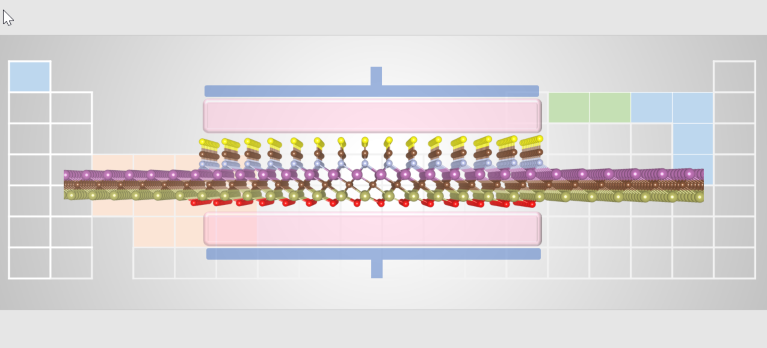
Concept of a functional-group-engineered MXene transistor. Credit: Professor Santanu Mahapatra
Transistors with low-resistive contacts can be made possible, after researchers developed a computational technique that helps identify two-dimensional MXene materials. MXene, in its simplest form, contain a layer of carbon or nitride atoms sandwiched between two layers of transition metal atoms1.
The technique has shown efficiency in detecting the right kind of materials after screening thousands of MXene materials, says a team at the Indian Institute of Science (IISc) in Bengaluru.
The simplest form of MXenes conduct electricity like metals and graphene. They come in a variety of colours and can be produced as one-nanometre thick single flakes or layers. But the possibility of tuning their electrical properties for transistor applications remained untapped.
To explore it, the scientists developed the high-throughput computational technique. They used it to screen more than 23,000 MXene materials stored in an open-access database previously developed by IISc.
The team, which included device engineers Santanu Mahapatra, Sirsha Guha and Arnab Kabiraj, assessed the MXenes’ electrical properties and potential for transistor applications. They chose the MXenes with non-magnetic metal atoms and detected 38 semiconducting ones.
The researchers say that the MXenes’ chemical structure offers low-resistive contacts with external metallic circuits that don’t require doping. They think that it may lead to a realistic solution for the sub-decananometer technology scaling for 2D material-based transistors.
In future, the approach can form a blueprint for screening and designing other 2D materials for various applications, the researchers note.
