Volume 10
-
No. 12 December 2011
It is shown that an elastic film on a viscoelastic substrate under biaxial compressive stress forms a hierarchical network of folds generated by repetitive wrinkle-to-fold transitions. The morphology of the hierarchical patterns can be controlled by modifying the geometry and boundary conditions of the film.
Letter p952; News & Views p907
IMAGE: PILNAM KIM, MANOUK ABKARIAN AND HOWARD A. STONE
COVER DESIGN: DAVID SHAND
-
No. 11 November 2011
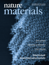
Monodisperse octapod-shaped inorganic nanocrystals suspended in suitable solvents are shown to self-assemble into chains of interlocked octapods, which in turn aggregate to form three-dimensional crystals. Such hierarchical self-assembly is supported by a simulation model of the octapods, which shows that the favourable interlocked configuration is encoded in the octapods shape.
Letter p872; News & Views p815
IMAGE: SERGIO MARRAS AND KAROL MISZTA
COVER DESIGN: DAVID SHAND
-
No. 10 October 2011
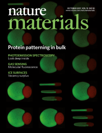
Bioactive proteins within hydrogel scaffolds used to culture cells can guide cellular activities, but the control of the location of the proteins in these three-dimensional structures has proved difficult. Using the multiphoton laser of a confocal microscope, simultaneous patterning of two growth factors, which remain bioactive after immobilization, is now shown. The technique should be applicable to the patterning of a variety of proteins.
Article p799, News & Views p727
IMAGE: KARYN HO AND RYAN G. WYLIE
COVER DESIGN: DAVID SHAND
-
No. 9 September 2011
Three-dimensional photonic devices are of interest as light emitters, detectors or waveguides. However, so far their fabrication has remained a challenge. The template-directed epitaxy of three-dimensional semiconductor structures now offers a new strategy for the realization of photonic devices, demonstrated by the realization of a three-dimensional photonic crystal light-emitting diode.
Article by Erik C. Nelson et al.
ERIK NELSON AND PAUL BRAUN
COVER DESIGN: DAVID SHAND
-
No. 8 August 2011
Plasmonic resonances are widely used for sensing applications. The plasmon resonance of a single nanoantenna structure is now used to detect changes in the dielectric properties of a nearby palladium nanoparticle exposed to hydrogen gas, enabling highly sensitive sensing in ultrasmall volumes. The approach can be easily extended to other sensing and catalysis schemes.
Article by Na Liu et al; News & Views by Roy Sambles et al.
SVEN HEIN, NA LIU AND HARALD GIESSEN
COVER DESIGN: DAVID SHAND
-
No. 7 July 2011
Nanowires have many applications across a number of disciplines. So far, their length has been largely limited to mesoscale dimensions. Through the adaption of an iterative fibre-drawing process it is now possible to fabricate millions of ordered nanowires and nanotubes of almost infinite length.
Cover image credit: UNAM-National Nanotechnology Research Center/Mehmet Bayindir
Letter by Yaman et al.
-
No. 6 June 2011
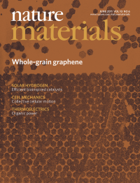
Chemical vapour deposition is a promising route for large-scale graphene growth. It is now shown that through the use of seeds high-quality, large, single-crystal domains can be grown on a patterned arrangement, and can be used to carefully study the transport across grain boundaries.
Cover image credit: Qingkai Yu and Yong P. Chen
Article Qingkai Yu et al. and News & Views by Pulickel M. Ajayan and Boris I. Yakobson
-
No. 5 May 2011
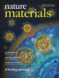
A nanocarrier - synthesized by the fusion of liposomes to spherical, nanoporous silica particles and by subsequent modification of the lipid bilayer with targeting peptides and fusogenic peptides - shows the targeted delivery and controlled release of chemically diverse multicomponent cargos within the cytosol of human liver carcinoma cells.
Cover image credit: Mona Aragon, Carlee Ashley and C. Jeffrey Brinker
News & Views by Irvine
-
No. 4 April 2011
Because nanotubes are generally prepared from their constituent elements at high temperatures, it is difficult to control their size, shape and electronic states. A bottom-up approach for the room-temperature fabrication of an assembly of infinite square-prism-shaped nanotubes with high tunability, using metal ions and organic molecules as building blocks, is now reported.
Image courtesy of Hiroshi Kitagawa.
Letter by Otsubo et al.
-
No. 3 March 2011
Transmission electron microscopy has reached unprecedented resolution and can provide structural information down to the single atomic level. It is now shown that a properly designed experimental analysis also allows the charge distribution around a single atomic dopant to be monitored, demonstrating the possibility of TEM to provide electronic as well as structural information.
Article by Meyer et al and News & Views by Urban
Focus
-
No. 2 February 2011
Metallic glasses are strong but are brittle once they yield. A novel Pd-based metallic glass now shows significantly enhanced fracture toughness. The unique combination of yield strength and toughness makes this glass comparable to the toughest as well as strongest materials known.
Article by Marios D. Demetriou et al.
-
No. 1 January 2011
The only way diamond can be polished is by pressing it against small diamond crystals, but this works well only for certain crystallographic orientations. The details of this wear mechanism have now been uncovered in simulations that suggest wear occurs via a thin amorphous layer on the diamond surface.
Cover design by David Shand.
Letter by Pastewka et al.
News & Views by Fineberg
Focus