The future of microelectronics
Vol.
406, No. 6799 (31 August 2000).
|![]() PDF
PDF![]() (209
(209![]() K)
K)![]() |
|
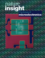 |
| Cover
illustration Set against repeated images of the world's first transistor, developed by Brattain and Bardeen in 1947, is a scanning electron microscopic view of phase-shifted 0.12-µm gates in one of today's state-of-the-art digital signal processors. (Images courtesy of Lucent Technologies' Bell Labs.) |
The remarkable success of the semiconductor
industry is well described by 'Moore's law', essentially a prescription for future
progress made back in 1965, which has held to the present day: every three years
will see a new generation of memory chips and microprocessors, in which the device
size will reduce by 33%, the chip size will increase by 50%, and the number of
components on a chip will quadruple. This has fuelled a thirst for cheaper electronic
memory and increasingly powerful microprocessors that has yet to be satisfied.
But such a trend cannot continue indefinitely; indeed, it is surprising to many that it has been sustained for as long as it has. For example, if the present miniaturization trend continues, the narrowest features on microelectronic circuitry will be only a few atoms across by the end of this decade. This collection of reviews will therefore focus on some of the most pressing technological and fundamental problems that are — or will be — faced by the semiconductor industry if it is to continue to satisfy the relentless consumer demand for speed and computational power.
Although this collection is not intended to be
comprehensive, we hope that it provides a flavour of the intellectual challenges
faced by the semiconductor industry and illustrates the multidisciplinary nature
of the endeavour. And by exploring issues of both a practical and fundamental
nature, we hope that this collection offers something to pure and applied scientists
alike.
Karl Ziemelis Physical Sciences
Editor
| The
drive to miniaturization PAUL S. PEERCY Following the introduction of silicon-based integrated circuitry over three decades ago, the integration density of such circuits has doubled every 12 to 18 months: this observation is known as Moore's law. For this historical trend to continue, significant challenges need to be overcome in several key technological areas. But for many of these challenges, there are at present no known solutions.
| 1023 | ||
| Pushing
the limits of lithography TAKASHI ITO AND SHINJI OKAZAKI The phenomenal rate of increase in the integration density of silicon chips has been sustained in large part by advances in optical lithography — the process that patterns and guides the fabrication of the component semiconductor devices and circuitry. Although the introduction of shorter-wavelength light sources and resolution-enhancement techniques should help maintain the current rate of device miniaturization for several more years, a point will be reached where optical lithography can no longer attain the required feature sizes. Several alternative lithographic techniques under development have the capability to overcome these resolution limits but, at present, no obvious successor to optical lithography has emerged.
| 1027 | ||
| Alternative
dielectrics to silicon dioxide for memory and logic devices ANGUS I. KINGON, JON-PAUL MARIA & S. K. STREIFFER The silicon-based microelectronics industry is rapidly approaching a point where device fabrication can no longer be simply scaled to progressively smaller sizes. Technological decisions must now be made that will substantially alter the directions along which silicon devices continue to develop. One such challenge is the need for higher permittivity dielectrics to replace silicon dioxide, the properties of which have hitherto been instrumental to the industry's success. Considerable efforts have already been made to develop replacement dielectrics for dynamic random-access memories. These developments serve to illustrate the magnitude of the now urgent problem of identifying alternatives to silicon dioxide for the gate dielectric in logic devices, such as the ubiquitous field-effect transistor.
| 1032 | ||
| Amplifying
quantum signals with the single-electron transistor MICHEL H. DEVORET AND ROBERT J. SCHOELKOPF Transistors have continuously reduced in size and increased in switching speed since their invention in 1947. The exponential pace of transistor evolution has led to a revolution in information acquisition, processing and communication technologies. And reigning over most digital applications is a single device structure — the field-effect transistor (FET). But as device dimensions approach the nanometre scale, quantum effects become increasingly important for device operation, and conceptually new transistor structures may need to be adopted. A notable example of such a structure is the single-electron transistor, or SET. Although it is unlikely that SETs will replace FETs in conventional electronics, they should prove useful in ultra-low-noise analog applications. Moreover, because it is not affected by the same technological limitations as the FET, the SET can approach closely the quantum limit of sensitivity. It might also be a useful read-out device for a solid-state quantum computer.
| 1039 | ||
| Ultimate
physical limits to computation SETH LLOYD Computers are physical systems: the laws of physics dictate what they can and cannot do. In particular, the speed with which a physical device can process information is limited by its energy and the amount of information that it can process is limited by the number of degrees of freedom it possesses. Here I explore the physical limits of computation as determined by the speed of light c, the quantum scale  and the gravitational constant G. As an example, I put quantitative bounds
to the computational power of an 'ultimate laptop' with a mass of one kilogram
confined to a volume of one litre.
and the gravitational constant G. As an example, I put quantitative bounds
to the computational power of an 'ultimate laptop' with a mass of one kilogram
confined to a volume of one litre.
| 1047 | ||
