
Thank you for visiting nature.com. You are using a browser version with limited support for CSS. To obtain the best experience, we recommend you use a more up to date browser (or turn off compatibility mode in Internet Explorer). In the meantime, to ensure continued support, we are displaying the site without styles and JavaScript.

Volume 7 Issue 10, October 2015

Research Highlight

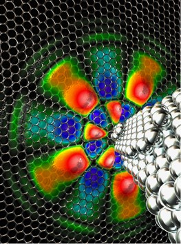
  • Recently, a research group from the Center for Nanoscale Science and Technology at the National Institute of Standards and Technology (NIST), and the Massachusetts Institute of Technology in the United States has demonstrated a new type of quantum electro-optic phenomenon, whispering-gallery mode resonators.1 The resonators are generated by a scanning tunneling microscope (STM) in proximity to graphene devices (Figure 1). On the basis of the quantum effect of electron tunneling, STM is a powerful technique to investigate the local electronic properties of both metallic and semiconducting systems with atomic resolution. Graphene, the most acclaimed material of the last decade, has enabled new horizons for STM research. The graphene surface can be directly probed by the scanning tip, whereas remaining chemically stable and clean even exposure to ambient air for days. Charged carriers in graphene can be readily tuned from holes to electrons using an external gate electrode. Furthermore, the charge carriers in graphene, often called Dirac particles, behave like electromagnetic waves, setting the stage for graphene to realize quantum electro-optic phenomena such as Veselago lensing2 and Klein tunneling.3

    • Suyong Jung
    Research Highlight Open Access

    Advertisement

Top of page ⤴

Original Article

  • Cd3As2, which is known as a topological Dirac semimetal, has been grown on mica substrates by molecular beam epitaxy with high mobility. The temperature-dependent resistance of as-grown Cd3As2 thin films showed semiconducting behavior, indicating the band gap opening as opposed to the bulk counterpart. By solid electrolyte gating, the ambipolar effect and gate-tunable quantum oscillations were clearly demonstrated. These features make the Cd3As2 thin film system a promising platform to observe various exotic phenomena and realize new electronic applications.

    • Yanwen Liu
    • Cheng Zhang
    • Faxian Xiu
    Original Article Open Access
  • A photovoltaic device based on a high-work-function metal/single-walled carbon nanotube (SWNT)/low-work-function metal hybrid junction was constructed to generate a strong built-in electric field in the SWNT for efficiently separating photogenerated electron-hole pairs. In the dark, the device behaved as a gate-dependent Schottky diode, with a high rectification ratio (Iforward/Ireverse) of >103 achieved for the device fabricated with an 1.4-nm-diameter SWNT. Under monochromatic illumination, this device exhibited an open-circuit voltage of 0.15 V and a high quantum efficiency of ~75%. It was found that the SWNT diameter had an important effect on the device characteristics.

    • Changxin Chen
    • Tiening Jin
    • Yafei Zhang
    Original Article Open Access
  • A heterogeneous palladium–silver alloy can catalyze selective methylation of aromatic amines under ambient pressure and without additives. Methylation of amines is used to manufacture chemicals used in fertilizers, fungicides, synthetic leathers and polymers. Formic acid, which is produced from biomass, is an environmentally friendly reagent for producing amines. They achieved complete conversion and high selectivities in the range 90–97% for methylation and dimethylation of various substituted aromatic amines only by formic acid as the source. The catalyst realized yields comparable to those of homogenous catalysts with acid additives for methylation with carbon dioxide and hydrogen under high pressure.

    • Ajay K Singh
    • Yoon-Ho Hwang
    • Dong-Pyo Kim
    Original Article Open Access
Top of page ⤴

Search

Quick links