Thank you for visiting nature.com. You are using a browser version with limited support for CSS. To obtain
the best experience, we recommend you use a more up to date browser (or turn off compatibility mode in
Internet Explorer). In the meantime, to ensure continued support, we are displaying the site without styles
and JavaScript.
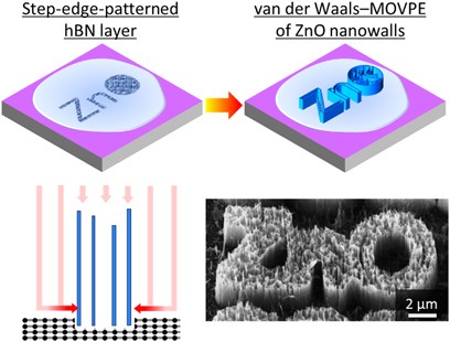
Architectured ZnO nanostructures were grown by van der Waals (vdW) heteroepitaxy on hexagonal BN (hBN) layers with artificially patterned atomic ledges. Electron microscopic and theoretical computational analyses presented non-covalent epitaxial features of domain-aligned incommensurate ZnO/hBN heterostructure. The vdW epitaxial ZnO/hBN heterostructures exhibited excellent electrical insulation of hBN, and were applied to fabricate the ultraviolet photodetector devices, as an example of functional optoelectronic device applications.
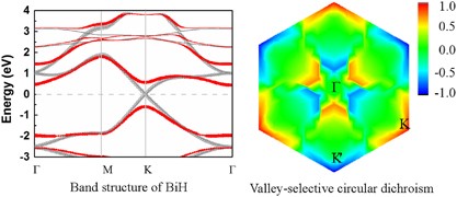
A group of 2D topological insulators BiX/SbX (X=H, F, Cl and Br) monolayers with extraordinarily large bulk gaps from 0.32 to a record value of 1.08 eV were predicated. These giant-gaps result from the strong spin-orbit interaction related to px and py orbitals of Bi/Sb atoms around the two valleys K and K′. The honeycomb structures of BiX monolayers remain stable even at a temperature of 600 K. The electric field-biased BiX/SbX monolayers become quantum valley Hall insulators, showing valley-selective circular dichroism. These features make the BiX/SbX monolayers an ideal platform to realize many exotic phenomena and fabricate new quantum devices.