Thank you for visiting nature.com. You are using a browser version with limited support for CSS. To obtain
the best experience, we recommend you use a more up to date browser (or turn off compatibility mode in
Internet Explorer). In the meantime, to ensure continued support, we are displaying the site without styles
and JavaScript.
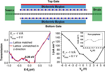
An electric field-enhanced transport gap is well established in a dual-gated field effect transistor (FET) based on the h-BN/single-layer graphene/h-BN sandwich structure, and the on/off current ratio is increased by a factor of 8.0 compared with pure single-layer graphene FET. The tunable and sizeable band gap and structural integrity render this sandwich structure a promising candidate for high-performance single-layer graphene FETs.
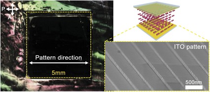
We describe a novel method for liquid crystal (LC) alignment using nano-patterns of electrically conductive indium–tin oxide (ITO) layers with high resolution (ca<20 nm) and high aspect ratio (ca 8), fabricated based on the secondary sputtering phenomenon. The ITO pattern developed in this manner can function as an electrode and alignment layer at the same time, which facilitates successful fabrication of bifunctional conductive alignment layer for LC devices.