Thank you for visiting nature.com. You are using a browser version with limited support for CSS. To obtain
the best experience, we recommend you use a more up to date browser (or turn off compatibility mode in
Internet Explorer). In the meantime, to ensure continued support, we are displaying the site without styles
and JavaScript.
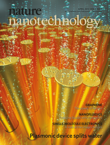
An abiding goal in solar-energy conversion is the fabrication of a small, artificial photosynthetic device that is able to carry out photocatalytic redox chemistry autonomously to create useful products such as fuel or fine chemicals. This artist's impression shows a plasmonic water-splitting device based on a gold nanorod array. On illumination with visible light all of the hydrogen is produced as a result of the reduction of water by hot electrons derived from surface plasmons.
Graphene has been chosen as one of the European Commission's billion-euro flagship projects and has cemented its central position in European research.
Without insurance the long-term sustainability of nanotechnology is questionable, but insurance companies are encumbered by their institutional memory of losses from the asbestos crisis and the absence of suitable actuarial models to measure the potential risks of nanotechnology. Here we propose a framework that supports the transfer of nanomaterial production risk to the insurance sector.
A recent book on risk in nanotechnology highlights the different forms of risk studies — analysis, perception and communication — and explores the relationships that exist between them. Chris Toumey reports.
The excitation of plasmons in nanostructured metallic electrodes generates short-lived highly energetic carriers that can be injected into the conduction band of a semiconductor and used to drive artificial photosynthesis.
By varying the distance between two electrodes bridged by a single molecule, the interaction between charges passing through the molecular junction and their mirror images in the metal contacts can be observed.
Ultrafast spin currents in iron-based heterostructures generate terahertz radiation bursts whose frequency can be tailored through structural engineering.
While the size of silicon transistors in conventional computers shrinks towards the atomic scale, the quantum states of atoms and quantum dots in silicon are being investigated for quantum information processing.
Advances in the understanding of Raman processes in graphene have made it an essential tool for studying the properties of this one-atom-thick carbon material.
Electrostatic forces drive mechanical reconfiguration of a photonic metamaterial and enable megahertz-frequency electric modulation of its optical properties.
Transport measurements in triple quantum dots reveal a bidirectional Pauli spin blockade, and that electron transport occurs through electronic states that are extended over the three dots.
Magnetic force microscopy imaging reveals that individual dislocations in antiferromagnetic NiO crystals show ferromagnetic behaviour originating from the local atomic-scale structure.
The flow of nanoscale liquids along the outer surface of solid nanowires at a scale of attolitres per second can be directly imaged with in situ transmission electron microscopy and explained through theoretical analysis.