Volume 6
-
No. 12 December 2011
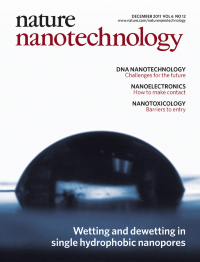
The behaviour of water in nanopores is very different from that of bulk water. For example, water can spontaneously evaporate if it is confined in a sufficiently narrow hydrophobic nanopore. Now Zuzanna Siwy and co-workers have shown that a single hydrophobic nanopore in a PET membrane can undergo reversible wetting and dewetting under the influence of an applied electric field, as predicted by molecular dynamics simulations. The nanopores are made hydrophobic by treating them with (trimethylsilyl)diazomethane. The cover is a photograph of a water droplet (which measures approximately 2 mm across) on a PET surface that has been treated in this way to make it hydrophobic.
Article p798; News & Views p759
COVER DESIGN: ALEX WING
-
No. 11 November 2011
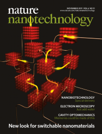
Materials that change their properties in response to external stimuli could have applications in electronics, sensing and catalysis. In the past, such switchable nanomaterials have relied on changes of shape to modify their properties, but now Bartosz Grzybowski and co-workers have shown that the electrical conductance of a film made of gold nanoparticles coated with charged ligands can be controlled by applying an electric field. This applied field sets up long-range gradients of both electrons (in the nanoparticle cores) and negative counterions (around the nanoparticles). Moreover, these gradients and the internal electric fields they create can be reconfigured to create different electronic elements. In this abstract representation, the nanoparticles are cubes, the currents between them are yellow and the conducting paths that have been switched off are copper coloured.
Article p740; News & Views p693
IMAGE: DAVID A. WALKER AND MARK SENIW
COVER DESIGN: ALEX WING
-
No. 10 October 2011
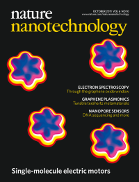
When a butyl methyl sulphide (BuSMe) molecule is absorbed on a metal surface it can rotate around the bond between the sulphur atom in the molecule and one of the metal atoms in the surface. Now Charles Sykes and co-workers have shown that electrons from a scanning tunnelling microscope (STM) can be used to drive directional motion of BuSMe molecules adsorbed on a copper surface. The direction and rate of the rotation are related to the chiralities of the molecule and the microscope tip. The BuSMe molecules shown here measure 2.5 nm across and appear hexagonal because of the symmetry of the underlying copper surface. The colours represent height (blue being the highest). This image was formed by duplicating an STM image of two BuSMe molecules.
Letter p625; News & Views p610
IMAGE: APRIL JEWELL AND HEATHER TIERNEY
COVER DESIGN: ALEX WING
Focus
-
No. 9 September 2011
Nanoscale optical antennas can concentrate light into volumes with subwavelength dimension, which is useful for applications such as solar cells, photodetectors and cancer therapy. Previously, however, it has not been possible to make absolute measurements of these enhanced electromagnetic fields in the near field. Now Edward Barnard, Ragip Pala and Mark Brongersma have developed a photodetector platform that can spectrally and spatially map the absolute values of the field near any type of nanoantenna by transducing the local electric fields into photocurrent. The image shows the theoretical enhancement of photocurrent by a metallic strip antenna (increasing from blue through white to red) as a function of wavelength (x axis) and the width of the strip (y axis).
Article p588
IMAGE: EDWARD S. BARNARD
COVER DESIGN: ALEX WING
-
No. 8 August 2011
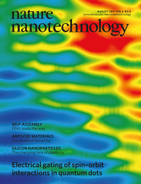
The ability to control the spins of electrons with electric fields is essential for the development of spintronic devices. Building on previous work in two-dimensional electron gases, Russell Deacon and co-workers have now shown that electric fields can be used to tune the strength of the Rashba interaction between the orbital motions and spin states of electrons in self-assembled InAs quantum dots. This false-colour image shows the differential conductance of the quantum dot as a function of applied magnetic field (horizontal axis) and gate voltage (vertical axis). The conductance reaches a maximum in the red regions and a minimum of zero in the blue regions.
Image: Russell Deacon and Yasushi Kanai
Cover design: Alex Wing
Article p511
-
No. 7 July 2011
Metamaterials are artificial materials with optical properties that are not found in naturally occurring materials, such as negative indices of refraction, and they are made by introducing nanoscale structure into conventional materials. John Rogers and co-workers now report that large areas of flexible high-quality negative-index metamaterials can be produced by 'printing' a multilayer stack consisting of alternate layers of silver and magnesium fluoride onto a substrate. The metamaterial shown in this colourized scanning electron micrograph is 430 nm thick; the image is 4.8 âμm wide.
Image credit: A. Jerez, Beckman Institute.
Letter p402; News & Views p396
-
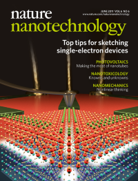
No. 6 June 2011
Devices that manipulate single electrons have applications in many areas of nanotechnology. The artist's impression on the cover shows the tip of an atomic force microscope creating a single-electron transistor at the interface between two oxide materials. Jeremy Levy and co-workers have used this approach to make a transistor in which single electrons tunnel between two nanowires through a conducting island with a diameter of just ~1.5 nm. The island (white circle at the bottom of the image), nanowires and other features are formed from a single oxide-based material that can be erased and rewritten, which is why the devices are called sketched oxide single-electron transistors.
Image credit: Guanglei Cheng.
Letter p343
-
No. 5 May 2011
Devices that manipulate single electrons have applications in many areas of nanotechnology. The artist's impression on the cover shows the tip of an atomic force microscope creating a single-electron transistor at the interface between two oxide materials. Jeremy Levy and co-workers have used this approach to make a transistor in which single electrons tunnel between two nanowires through a conducting island with a diameter of just ~1.5 nm. The island (white circle at the bottom of the image), nanowires and other features are formed from a single oxide-based material that can be erased and rewritten, which is why the devices are called sketched oxide single-electron transistors.
Image credit: Guanglei Cheng.
Letter p343
-
No. 4 April 2011
Single nuclear spins cannot be detected unless they are strongly coupled to an electron spin. Now Ren-Bao Liu and colleagues have shown that pairs of nuclear spins can be detected if they are strongly coupled to each other and only weakly coupled to an electron spin in a nitrogen vacancy in diamond. This false-colour image shows the coherence of the electron spin as a function of time (vertical axis) and angle (horizontal axis); the oscillations in the image are caused by a pair of nuclear spins that is 1.3 nm from the vacancy and act as a 'fingerprint' that can be used to identify a hidden dimer.
Image credit: Nan Zhao
Letter p242
-
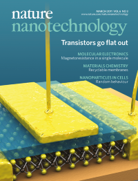
No. 3 March 2011
Improving the performance of field-effect transistors (FETs) involves reducing the length and thickness of the channel between the source and drain electrodes. Andras Kis and co-workers have made an FET in which the channel is a single layer of MoS2 that is just 0.65 nm thick and 1,500 nm long: the black spheres in this schematic (which is not to scale) are Mo atoms; the yellow spheres are S atoms. The MoS2 layer also has a bandgap, which is crucial for many applications.
Image credit: Andras Kis
Letter p147; News & Views p135
-
No. 2 February 2011
Mesoporous structures with well-ordered nanoscale channels could be used in a variety of applications, but our understanding of the growth of such structures through self-assembly is incomplete. Now Jens Michaelis, Christoph Bräuchle and co-workers have observed the self-assembly of a mesoporous silica film in real time using fluorescence polarization imaging and atomic force microscopy (AFM). This AFM image has been overlaid with white lines showing the direction of the pores as determined from the polarization images.
Image credit: Peter Schwaderer
Letter p87
-
No. 1 January 2011
Tissue engineering involves the development of functional substitutes for damaged tissues and organs. In this issue Tal Dvir, Brian Timko, Daniel Kohane and Robert Langer review the challenges involved in applying nanotechnology to tissue engineering. The foreground of this image is an artist's impression showing polymeric fibres (purple) engineered to recreate the cell microenvironment; the background is a scanning electron micrograph of an electrospun polymeric fibre mesh. The cells are shown in light blue.
Image courtesy of Bozhi Tian
Review Article p13