
Thank you for visiting nature.com. You are using a browser version with limited support for CSS. To obtain the best experience, we recommend you use a more up to date browser (or turn off compatibility mode in Internet Explorer). In the meantime, to ensure continued support, we are displaying the site without styles and JavaScript.

Volume 6 Issue 3, March 2011

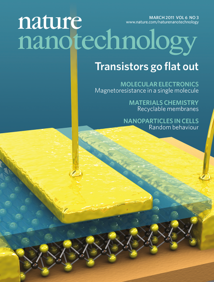
Improving the performance of field-effect transistors (FETs) involves reducing the length and thickness of the channel between the source and drain electrodes. Andras Kis and co-workers have made an FET in which the channel is a single layer of MoS2 that is just 0.65 nm thick and 1,500 nm long: the black spheres in this schematic (which is not to scale) are Mo atoms; the yellow spheres are S atoms. The MoS2 layer also has a bandgap, which is crucial for many applications.

Image credit: Andras Kis

Letter p147; News & Views p135

Research Highlights

Top of page ⤴

News & Views

  • The presence of a large bandgap means that a single layer of molybdenum disulphide can be used to make field-effect transistors with high on/off ratios and reasonably high mobilities.

    • Frank Schwierz
    News & Views
  • Recyclable membranes that are capable of separating nanoparticles of different sizes can be prepared from supramolecular assemblies that are held together by non-covalent bonds.

    • Carsten Schmuck
    News & Views
  • A statistical model based on a quantitative structure–activity relationship accurately predicts the cytotoxicity of various metal oxide nanoparticles, thus offering a way to rapidly screen nanomaterials and prioritize testing.

    • Enrico Burello
    • Andrew Worth
    News & Views
  • Statistical analysis of nanoparticle delivery shows that cells take up nanoparticles randomly and redistribute them to their daughter cells in a biased way.

    • Haruhisa Kato
    News & Views
Top of page ⤴

Letter

Top of page ⤴

Article

  • The contact resistance of a junction between graphene and palladium is shown to be strongly affected by carrier transport in graphene underneath the palladium, and is measured to be just two to three times larger than the minimum resistance achievable.

    • Fengnian Xia
    • Vasili Perebeinos
    • Phaedon Avouris
    Article
  • A single magnetic molecule between ferromagnetic contacts exhibits a 60% magnetoresistance effect and nearly metallic conduction at the same time.

    • Stefan Schmaus
    • Alexei Bagrets
    • Wulf Wulfhekel
    Article
Top of page ⤴

Corrigendum

Top of page ⤴

Search

Quick links