Thank you for visiting nature.com. You are using a browser version with limited support for CSS. To obtain
the best experience, we recommend you use a more up to date browser (or turn off compatibility mode in
Internet Explorer). In the meantime, to ensure continued support, we are displaying the site without styles
and JavaScript.
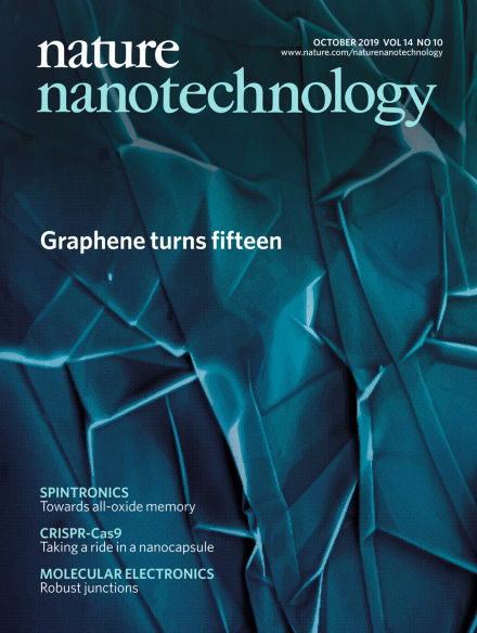
Since the first report of the isolation of atomically thin carbon films in 2004, the field of graphene and other 2D materials has expanded dramatically. Fast forward 15 years, graphene — once established as the world's thinnest, strongest and most conductive material — remains the subject of rigorous scientific scrutiny and significant industrial interest. More than a decade of fundamental research combined with the mature graphene manufacturing methodology have created a strong basis for the future commercialization of graphene. As a reminder of the old times when graphene was still prepared by repeated peeling of graphite, the cover art shows a scanning electron microscopy image of graphene flakes — small in size, big on scientific implications.
Visiting a research centre specialized in nanoscience and nanotechnology can be an inspiration for students in other disciplines, as Chris Toumey explains.
An EU-funded open call aims at building a consortium to bridge basic and applied research on graphene and related atomically thin crystals for the development of integrated circuit technologies.
Energy-efficient magnetization manipulation is a prerequisite for competitive spintronic devices. The Weyl semimetal WTe2 can act as a spin current source that enables magnetization switching of an adjacent ferromagnet at low power consumption and additionally induces chiral magnetism.
All-electrical switching of magnetization holds promise for applications in information technologies with low power consumption. Here, current-induced spin–orbit torque switches the magnetization in SrIrO3/SrRuO3 bilayer structures at 70 K in the absence of an external magnetic field.
The Weyl semimetal WTe2 possesses strong spin–orbit coupling and time-reversal-protected spin polarization in surface and bulk states. In a WTe2/permalloy heterostructure, WTe2 can act as a spin current source that enables magnetization switching at low current densities.
In situ investigation of a single nanowire/quantum dot heterojunction solar cell using a custom-designed photoelectric transmission electron microscope set-up reveals the possibility of achieving improved photovoltaic performance.
Mechanically and electronically stable graphene/molecule/graphene devices can be fabricated by combining a covalent binding of the molecules to the substrate with an optimized intermolecular π–π interaction.
Controlled delivery of neuromodulators in the brain might improve the understanding of the molecular basis of behaviour. In this letter, magnetic liposomes injected in deep brain regions release small molecules under remote magnetic stimulation, activating specific neuronal circuits in freely moving mice.
Polymer nanocapsules, assembled around a ribonucleoprotein complex of Cas9 nuclease and a single-guide RNA, enable safe and efficient gene editing in vitro and in vivo.
An imaging technique can acquire surface-enhanced Raman scattering intensity fluctuations at 800,000 frames per second, revealing the dynamics of plasmonic hotspots at the single-particle level.