
Thank you for visiting nature.com. You are using a browser version with limited support for CSS. To obtain the best experience, we recommend you use a more up to date browser (or turn off compatibility mode in Internet Explorer). In the meantime, to ensure continued support, we are displaying the site without styles and JavaScript.

Volume 20 Issue 11, November 2021

Nano-strutted tube-in-tube carbon lattice

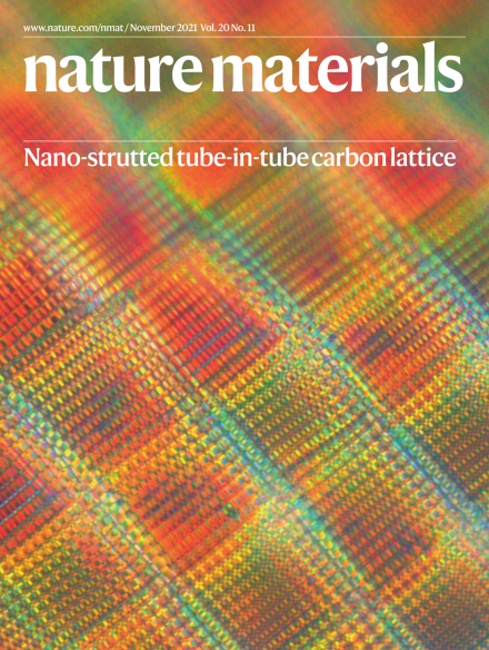
A nanoscale tube-in-tube sandwich structure is generated by a two-step templating-pyrolysis process, which strengthens the log-pile carbon architecture and slows down the decrease of stiffness with decreasing density.

See Ye et al.

Image: Jianchao Ye, Lawrence Livermore National Laboratory Cover Design: Thomas Phillips

Editorial

  • Nanoarchitecture design of materials offers great opportunities to achieve unusual properties, but requires fabrication techniques that ensure sufficient resolution and material quality.

    Editorial

    Advertisement

Top of page ⤴

News & Views

  • Nanoarchitected carbon composed of intricate tube-in-tube beams connected with nanostruts has been fabricated, achieving both ultralightweight and ultrahigh modulus.

    • Yujia Wang
    • Xiaoyan Li
    News & Views
  • A transparent suspension containing colloidal silica is used to additively manufacture three-dimensional structures and photonic devices of silica glass at the nanoscale.

    • Paolo Colombo
    • Giorgia Franchin
    News & Views
  • Centimetre-scale crack-free metal nanolattices are realized, enabling outstanding high tensile strength in low-density materials.

    • Andreas Stein
    • Nathan A. Mara
    News & Views
  • Passivation of traps via site-specific surface doping allows access to the intrinsic properties of organic semiconductors and leads to the observation of electron atmospheres in organic crystals.

    • Oana D. Jurchescu
    News & Views
  • A functional bioadhesive has been developed to possess properties such as mechanical compliance, electrical conductivity and optical transparency, and is utilized for bonding electronic devices to various organs in the body for up to several months.

    • Tsuyoshi Sekitani
    News & Views
Top of page ⤴

Perspectives

Top of page ⤴

Letters

  • Atomic-scale visualization of the superfluid velocity field, the electron-pair density and the superfluid current density in an electron-pair superfluid surrounding an Abrikosov vortex in a superconducting sample of NbSe2 is demonstrated, using superconducting-tip scanning tunnelling microscopy.

    • Xiaolong Liu
    • Yi Xue Chong
    • J. C. Séamus Davis
    Letter
Top of page ⤴

Articles

Top of page ⤴

Amendments & Corrections

Top of page ⤴

Search

Quick links