Thank you for visiting nature.com. You are using a browser version with limited support for CSS. To obtain
the best experience, we recommend you use a more up to date browser (or turn off compatibility mode in
Internet Explorer). In the meantime, to ensure continued support, we are displaying the site without styles
and JavaScript.
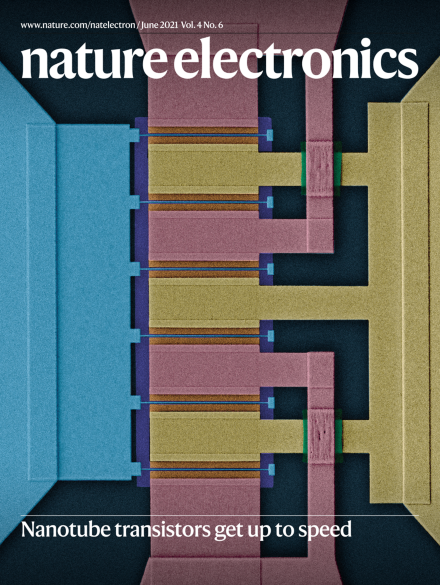
High-speed transistors that are based on arrays of aligned carbon nanotubes could potentially be scaled for operation in millimetre-wave and terahertz frequencies. The cover shows a scanning electron microscopy image of a six-finger nanotube transistor that is fabricated on a silicon wafer and can be used to build a radiofrequency amplifier.
Two-dimensional structures that are engineered to manipulate electromagnetic radiation are becoming increasingly practical and could be of use in bioelectronics and communications.
This Review examines the development of metasurfaces for bioelectronic interfaces, exploring how they can be used to control electromagnetic fields in the vicinity of the human body and their potential application in current and emerging healthcare technologies.
Domain wall devices based on perpendicular magnetic tunnel junctions with a hybrid free layer design can offer electrical read and write, and fast domain wall motion driven via spin–orbit torque.
Transistors based on arrays of aligned carbon nanotubes can exhibit cutoff frequencies of up to 540 GHz, and could be further scaled for operation at millimetre-wave and terahertz frequencies.
Boron arsenide and boron phosphide cooling substrates can be integrated with other materials, including the wide-bandgap semiconductor gallium nitride, creating structures that exhibit high thermal boundary conductances and high-electron-mobility transistors that exhibit low hot-spot temperatures.
Electrically tunable metamaterial-inspired devices in the microwave range can be created by using resonators that are integrated with organic electrochemical transistors and are entirely fabricated via inkjet-printed onto polyimide substrates.
A tactile sensing system that can learn to identify different types of surface can be created using sensors that mimic the fast and slow responses of mechanoreceptors found in human skin.
A microstrip patch antenna array and a single high-electron-mobility transistor, which are created with inkjet printing, can be used for backscatter communication at millimetre-wave frequencies, providing a bit rate of two gigabits per second and with a front-end energy consumption of only 0.17 pJ per bit.