Thank you for visiting nature.com. You are using a browser version with limited support for CSS. To obtain
the best experience, we recommend you use a more up to date browser (or turn off compatibility mode in
Internet Explorer). In the meantime, to ensure continued support, we are displaying the site without styles
and JavaScript.
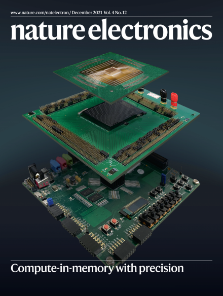
A compute-in-memory macro that is based on complementary metal–oxide–semiconductor (CMOS) technology and resistive random-access memory can be used for precise and efficient neural network implementation. The photograph on the cover shows the compute-in-memory chip (top), interconnect breakout boards (middle) and the field-programmable gate array (FPGA) control board (bottom).
Technology breakthroughs at the 2021 IEEE International Electron Devices Meeting, which is once again being held as an in-person event in San Francisco.
Han Wang and H.-S. Philip Wong of the Taiwan Semiconductor Manufacturing Company (TSMC) tell Nature Electronics about the company’s research efforts into two-dimensional materials.
A monolithic three-dimensional integrated system based on CMOS logic, compute-in-memory and associative memory can be used to efficiently implement one-shot learning.
Monolayer transition metal dichalcogenide transistors can be fabricated on 300 mm wafers using an approach that is compatible with back-end-of-line process temperatures.
Inorganic molecular crystal films of antimony trioxide can be grown on 4-inch wafers via a thermal evaporation process and used as a top-gate oxide in two-dimensional molybdenum disulfide transistors.
This Review examines the scaling prospects of quantum computing systems based on silicon spin technology and how the different layers of such a computer could benefit from using complementary metal–oxide–semiconductor (CMOS) technology.
An on-chip device that is based on a Josephson junction coupled to a fabricated superconducting resonator can provide a source of coherent microwave radiation for potential use in scaled quantum circuits.
Measurements of inkjet-printed thin-film devices made from titanium carbide MXene (metal), molybdenum disulfide (semiconductor) and few-layer graphene (semimetal) clarify the charge transport mechanisms of the devices and highlight the role of inter-flake and intra-flake processes.
Inorganic molecular crystal films of antimony trioxide can be fabricated using thermal evaporation deposition and used as a van der Waals dielectric in molybdenum disulfide field-effect transistors.
A vertical transistor and resistive memory can be integrated on a single vertical III–V semiconductor nanowire on silicon, creating a compact cell capable of Boolean logic operations.
Advanced complementary metal–oxide–semiconductor technology and resistive random-access memory can be used to create high-bit-precision compute-in-memory macros for low latency and efficient edge computing.