Volume 3
-
No. 12 December 2020
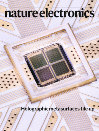
Holographic metasurfaces tile upUsing arrays of complementary metal–oxide–semiconductor (CMOS)-based chip tiles, programmable metasurfaces can be created that are capable of holographic projections at terahertz frequencies. The photograph on the cover shows a metasurface that is made from a 2 × 2 array of tiles and contains 576 meta-elements, each of which is individually reconfigurable.
See Venkatesh et al.
-
No. 11 November 2020
Fluoride interfaces give perovskites the green lightUsing mixed-dimensional perovskites that are deposited on a polymeric hole-transport layer coated with a thin layer of lithium fluoride, green light-emitting diodes (LEDs) can be created with external quantum efficiencies of up to 19.1%. The illustration on the cover highlights the crystal structure of the perovskite LEDs.
See Zhao et al.
-
No. 10 October 2020
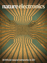
Artificial neural networks in 2DMultilayers of the two-dimensional material hexagonal boron nitride (h-BN) can be employed as the resistive switching material in high-density memristive crossbar arrays, creating devices that can be used to model an artificial neural network for image recognition. The cover shows an optical microscopy image of a 10 × 10 memristor crossbar array, which has a vertical metal/h-BN/metal structure.
See Chen et al.
-
No. 9 September 2020
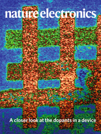
A closer look at the dopants in a deviceAtomically thin n-type and p-type dopant layers in silicon devices can be non-destructively imaged using broadband electrostatic force microscopy. The cover shows an electrostatic force microscopy image of patterned stripes (around 500 nm wide) of phosphorus dopant atoms, where the vertical stripes are buried 4 nm beneath the surface of the silicon substrate and the horizontal stripes at 9 nm.
See Gramse et al.
-
No. 8 August 2020
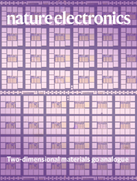
Two-dimensional materials go analogueOperational amplifiers can be fabricated from two-dimensional molybdenum disulfide field-effect transistors and used to create analogue feedback circuits such as inverting amplifiers, integrators, log amplifiers and transimpedance amplifiers. The cover shows an optical microscopy image of a chip containing these operational amplifiers (each with a footprint of around 0.04 mm2), as well as test transistors.
See Polyushkin et al.
-
No. 7 2 July 2020
Flexible chips hardwired for machine learningA flexible processor chip that has hardwired parameters for machine learning and contains around 1,000 logic gates can be built using a commercial 0.8-μm metal-oxide thin-film transistor technology. The schematic illustration on the cover highlights the flexible nature of the chips, which can be used in smart applications such as odour recognition.
See Ozer et al. and News & Views by Liu et al.
-
No. 6 June 2020
In-memory computing finds a new dimensionUsing 760,000 phase-change memory devices, an in-memory hyperdimensional computing system can be created that can perform machine learning tasks such language classification. Hyperdimensional computing takes inspiration from the brain and uses the mathematical properties of hyperdimensional spaces comprised of high-dimensional binary vectors known as hypervectors. The schematic illustration on the cover highlights these hypervectors (represented as cylinders) and the quasi-orthogonality of large hypervectors; the elements of the hypervectors are encoded using different atomic arrangements of small volumes of phase-change material (represented here with different ball-and-stick structures).
See Karunaratne et al.
-
No. 5 May 2020
Metal oxide gas sensors extend their rangeAn impedance measurement technique that is based on dielectric excitation at specific frequencies can improve the performance of semiconducting metal oxide gas sensors, providing a linear sensing signal over a wide range of gas concentrations. The cover shows a photograph of an integrated circuit impedance analyser (front) and three gas-sensing chips that can be used in the measurements.
See Potyrailo et al. and News & Views by Lee.
-
No. 4 April 2020
Memristors in 3DEight layers of memristors can be monolithically integrated on a chip to create a three-dimensional circuit capable of implementing a convolutional neural network. The cover shows a false-colour scanning electron microscopy image of part of the memristor array.
See Lin et al.
-
No. 3 March 2020
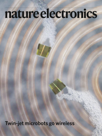
Twin-jet microbots go wirelessWireless power can be used to control the motion of flexible microbots that are composed of two tube-shaped catalytic micro-engines supported on a flat polymeric structure and have integrated coils to allow wireless energy transfer via inductive coupling. The cover shows an optical image of two of these microbots swimming in an aqueous solution above the coil used to transfer energy, and trailed by oxygen microbubbles that are used by the catalytic engines to provide propulsion.
See Article by Bandari et al. and News & Views by Xu et al.
-
No. 2 1 February 2020
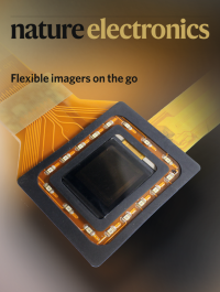
Flexible imagers on the goA thin and flexible image sensor, which combines polycrystalline silicon thin-film transistor readout circuits and organic photodiodes with high sensitivity in the near-infrared region, can be used to capture images of fingerprints and veins, and to map pulse waves. The cover shows a photograph of the wearable imager, which is set up to image a vein by attaching it directly to the skin.
See Yokota et al.
-
No. 1 January 2020
Air-gap gates feel the pressureSensitive pressure sensors, created by integrating a microstructured air-gap gate with two-dimensional semiconductor transistors, can be used to perform static pressure mapping, real-time human pulse wave measurements, sound wave detection and remote pressure monitoring. The cover shows a photograph of a 5 × 5 sensor array being used to weigh a red bean, a soybean and a grain of rice.
See Huang et al.