Thank you for visiting nature.com. You are using a browser version with limited support for CSS. To obtain
the best experience, we recommend you use a more up to date browser (or turn off compatibility mode in
Internet Explorer). In the meantime, to ensure continued support, we are displaying the site without styles
and JavaScript.
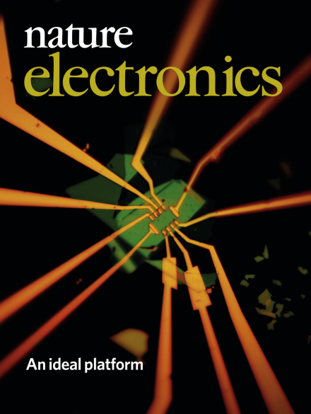
A device platform that uses transferred contacts made from a hexagonal boron nitride layer with embedded metal can create two-dimensional transistors with near-ideal device characteristics. The cover shows an optical microscopy image of a field-effect transistor made from bilayer tungsten diselenide built using the platform.
Research in both academia and industry is required to develop new and innovative technologies — though the differing goals of the two arenas can cause conflict.
A flexible phased array that has an areal mass density of only 0.1 g cm–2 could help deliver a new era of lightweight, portable and reconfigurable communication systems.
The topological Hall effect is observed at above room temperature in a bilayer heterostructure composed of thulium iron garnet and platinum, suggesting the formation of skyrmions in a magnetic insulator through the interfacial Dzyaloshinskii–Moriya interaction.
Bilayer WSe2 field-effect transistors with near ideal device characteristics can be created using transferred via contacts made from metal-embedded hexagonal boron nitride.
By combining a CMOS-based integrated circuit with flexible and collapsible radiating structures, a scalable phased array architecture can be fabricated that has an areal mass density of only 0.1 g cm−2.