
Abstract
Opening a sizable band gap without degrading its high carrier mobility is as vital for silicene as for graphene to its application as a high-performance field effect transistor (FET). Our density functional theory calculations predict that a band gap is opened in silicene by single-side adsorption of alkali atom as a result of sublattice or bond symmetry breaking. The band gap size is controllable by changing the adsorption coverage, with an impressive maximum band gap up to 0.50 eV. The ab initio quantum transport simulation of a bottom-gated FET based on a sodium-covered silicene reveals a transport gap, which is consistent with the band gap and the resulting on/off current ratio is up to 108. Therefore, a way is paved for silicene as the channel of a high-performance FET.
Introduction
Owing to its extremely high carrier mobility, graphene has attracted enormous attention since its discovery in 20041. However, pure graphene is not suitable for effective field effect transistor (FET) operating at room temperature due to its zero band gap. Opening a sizable band gap without degrading the electronic properties is critical for the application of graphene in nanoelectronics and is probably one of the most important and tantalizing research topics of the graphene community. Any successor to silicon metal-oxide-semiconductor FET (MOSFET) that is used in complementary MOS-like logic must have a sizeable band gap of 0.4 eV or more and an on-off current ratio between 104 and 107 2. Unfortunately, the opened band gap without degrading the electronic properties in graphene (via a vertical electric field, molecular surface adsorption, or hexagonal boron nitride (h-BN) as a substrate) is usually smaller than 0.34 eV3,4,5,6,7,8 and the observed on-off current ratio at room temperature is no more than 1009. Silicene, graphene analogue for silicon, is predicted to be a zero band gap semiconductor with a Dirac cone as observed in graphene10,11. The synthesis of silicene on the Ag surface12,13,14,15,16,17 or zirconium diboride thin film18 has already been reported in several experiments. Recently, the linear band dispersion near the Fermi level has been observed in a silicene sample on Ag(111) surface by angle-resolved photoemission spectroscopy (ARPES), unambiguously verifying the existence of silicene12. With its massless Dirac Fermions character, extremely high carrier mobility is expected in silicene as in graphene. Therefore, silicene is a promising material for high-speed switching devices. Apparently, pure silicene cannot directly be used for effective FETs either because of the same cause as graphene19.
Although covalent functionalization20,21,22 or epitaxial growth in the form of nanoribbon15,16 can open a sizable band gap in silicene, the electronic properties are destructed and the carrier mobility is inevitably decreased to a large extent, as happened in graphene23,24. Therefore, opening a sizable and tunable band gap of silicene without degrading the electronic properties is equally highly desired for high-performance silicene FET devices. It is proposed that a vertical electric field can open a tunable band gap in silicene without degrading the electronic properties19. However, the maximum opened band gap by the experimentally accessible electric field is just 0.13 eV. Moreover, a single-gated device is desirable from the device point of view25. Very recently, it is reported that silicene that epitaxial grown on Ag surface or zirconium diboride thin film can open a band gap of about 0.6 or 0.3 eV, respectively12,18. However, Ag is an metal substrate, which is undesired in a FET device and the calculated dispersion relation near the band gap for silicene on zirconium diboride thin film is very flat, which will lead to a rather large carrier effective mass and greatly decrease the carrier mobility. Besides, the size of the band gap of silicene opened by the interaction with substrate is difficult to tune.
In this Article, based on the density functional theory (DFT) calculations we propose that the band gap of silicene can be opened without degrading the electronic properties by surface adsorption of alkali metal (AM). The band gap is tunable by controlling the coverage of AM. Most intriguingly, the maximum band gap is up to 0.50 eV by adsorption of AM atoms, which meets the band gap requirement of high-performance FETs. Subsequently, a bottom-gated FET device based on a sodium-covered silicene monolayer is simulated by the ab initio transport calculations. A sizable transport gap and a high on/off current ratio (~ 108) are available in this device, suggestive of the great potential of silicene as the channel of a high-performance FET.
Results
The supercell model consists of an m × m primitive silicene cell (m = 1, , 2, 3 and 4) and an AM atom (AM = Li, Na, K, Rb and Cs) on the top. The AM-covered silicene is denoted as AMSin, where n is the number of the silicon atom per supercell. We define the coverage N of the AM on silicene as the ratio of the number between the AM and Si atoms per supercell and one has N = 1/n. The in-plane lattice constant of silicene is taken from that of previous works, a = b = 3.866 Å10,26,27. Along the z-direction perpendicular to the silicene plane, the lattice constant of 30 Å is used.
Geometry and stability
Of all the examined adsorption sites, the AM atoms favor sitting above the hexagonal ring center of silicene and have the highest sixfold coordination (Fig. 1). Such a sixfold coordination configuration of the AM atom has been reported to be favorable in a AM-covered graphene28. A metastable state, in which the AM atoms all sit above the bottom Si atom, is available (Supplementary Fig. S1). The energy differences between these two states increase from 0.06 to 0.21 eV with the decreasing coverage, which are larger than the room temperature (~ 0.026 eV) and thus ensure the thermodynamically stability and reliable operation if the AM-covered silicene is fabricated as the FET channel.

Structures of the Na-covered m × m silicene supercell.
(a–e) The adsorption coverage is N = 3.1%, 5.6%, 12.5%, 16.7% and 50.0%, respectively, for m = 4, 3, 2,  and 1. The rhombi plotted in black line represent the supercells at different coverages. (f) Top and side views of an Na-covered silicene supercell over the h-BN sheet with N = 12.5%. d0: the silicene buckling; d1: the distance between Na and the top-surface silicene; d2: the distance between h-BN and the bottom-surface of silicene.
As shown in Supplementary Fig. S2, the silicene buckling (d0) increases from 0.46 to 0.49 ~ 0.77 Å after the AM adsorption, weakly dependent on the AM species and the coverage. On the contary, the distance of the AM atom to the silicene top-surface (d1) singnificantly ranges from 1.3 to 2.8 Å with the increasing atomic radius of AM, but nearly independent of the coverage N.
We define the adsorption energy of the AM atom on silicene as

where ESi, EAM and ESi+AM are the relaxed energy for silicene, the isolated AM atom and the combined system, respectively. As shown in Fig. 2a, the Ea values are positive with magnitudes of 0.57 ~ 2.92 eV per AM atom, showing that the AM one-side adsorption on silicene layer is always strongly or moderately exothermic. Ea tends to reduce with the increasing N. One cause is that the electrostatic attraction between the AM atom and silicene is reduced with the increasing N, as a result of the reduced charge transfer Q from the AM cation and silicene (Fig. 2b). Another cause is the repulsion between the AM cations and silicene increases with the increasing N. We notice that although the transferred Q from Li to silicene is apparently smaller than those from other AM atoms, Ea of Li on silicene is comparable with those of other AM atoms on silicene. This suggests an evident ‘covalent component’ of Li-Si interaction besides the ionic contribution29.

(a) Adsorption energy, (b) Mulliken charge transferred from the adatom to silicene, (c) band gap and (d) effective mass of electrons of the AM-covered silicene as a function of the coverage N.
Lines connecting symbols are guides to the eye.
Electronic structure
Given the same coverage, silicene covered by different AM species share similar electronic structures. We select Na-covered silicene as a representative and show its electronic structure at different coverages in Fig. 3. Even at the smallest coverage of N = 3.1%, a small direct band gap of 0.04 eV is opened between the π and π* states while the Dirac cone shape is almost preserved (Fig. 3a). Due to the heavy electron doping, the Fermi level (Ef) is elevated by 0.50 eV with respect to the valence band maximum (VBM). The band gap at the Dirac point is increased monotonically to 0.08, 0.17, 0.30 and 0.45 eV at N = 5.6, 12.5, 16.7 and 50%, respectively (Fig. 3b–3e). Notably, both of the two original Dirac points Ks and  in silicene are folded to the
  point of the reduced first Brillouin zone (BZ) at N = 5.6% (
 supercell) and 16.7% (3×3 supercell), as shown in Fig. 3b and 3d, respectively. The opened maximum band gap has already met the requirement of 0.4 eV for practical FETs operation. At N = 12.5 and 50%, there is a band across Ef around the Γ point, which mainly originates from the broaden outmost 3s valence orbital of the adsorbed Na atoms (The inset of Fig. 3e).

Band structures of the Na-covered silicene at different coverages.
The Dirac point in (b) and (d) is folded to the Γ point due to the reduction of the first Brillouin zone. The red dashed-line in (c) stands for the band structure of the Na-covered silicene with an h-BN buffer layer. Inset of (e): Orbital of the conduction band bottom at the Γ point. The Fermi level is set to zero.
Fig. 2c shows the band gap change with the coverage N of the five kinds of the AM-covered silicene. Given a coverage N, the band gaps induced by different AM species adsorption are similar except for the LiSi9 and LiSi6 monolayers, the latter of which has an extraordinary large band gap of 0.46 eV, compared with a value of about 0.2 eV for other AM-covered silicene at this coverage. The band gaps of all the five kinds of AM-covered silicene monolayers increase generally with the increasing coverage, with values ranging from 0.04 to 0.50 eV.
It has been established that a vertical electric filed can induce a band gap in silicene because it breaks the sublattice symmetry in silicene19. The AM adsorption leads to a charge transfer between AM and silicene, which builds a perpendicular electric field in silicene. This perpendicular electric field breaks the sublattice symmetry and thus opens a band gap in silicene. The asymmetry between the two sublattices increases with the increasing coverage and the band gap is correspondingly increased. We should notice a similar phenomenon and band gap opening mechanism in bilayer graphene. Both experiments4,8,25 and theoretical calculations5,30 reveal that a band gap can be opened in bilayer graphene via single-side adsorption of metal atoms or acceptor/donor molecules because a vertical electric field is built in bilayer graphene due to a charge transfer occurs between the adsorbate and bilayer graphene and it breaks the inversion symmetry of bilayer graphene. The size of the band gap can be controlled by changing the adsorption concentration. Besides the breaking of sublattice symmetry, we point out that the breaking of the bond symmetry also contributes to the band gap opening in the AM-covered silicene. Let us recall its single layer graphene counterpart. When adsorbed on single layer graphene, the Li atoms are also located above the hexagon center of single layer graphene (notated as LiCn), just like the case happened in silicene. If and only if in some certain coverages (n = 3x, x is an arbitrary integer) and the corresponding supercell take forms like  , 3×3, etc. (The lattice constant is their integral multiple), the bond symmetry is broken, resulting in a Kekulé ordering. Finally, a band gap is created in the LiC3x monolayer though the sublattice symmetry of single layer graphene is well preserved31.
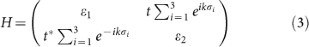
In an AMSin monolayer, when n = 3x, the second band gap opening mechanism also works. It is convenient to interpret this mechanism using the tight-binding model with the Hamiltonian

where  and ci are the fermionic creation and annihilation operators on site i,
  the on-site energy and tij the hopping amplitudes. Following this model, we can divide the effects of AM-adsorption into two parts:
-
1
Breaking of sublattice symmetry. The on-site energies εi are equal in the pure silicene. Due to the charge transfer between AM and silicene, a perpendicular electric field is built in silicene. Because there is buckling in silicene, the Coulomb fields felt by the top and bottom sublattices are different, resulting to a split of εi. We notate the on-site energy of the two sublattices as ε1 and ε2, respectively. The eigen function can be approximately expressed as a linear combination of the normalized pz orbitals of Si atoms. We consider the most simple case of n = 2 of the AMSin monolayer and the Hamiltonian is given by
where the vectors σi connect the two sublattices of silicene (Fig. 4c). In the Dirac points (
 ), the opened band gap can be written as
Only if n ≠ 3x, the band gap always can be expressed as the function of the on-site energy εi. The
 discrepancy between the two sublattices is also responsible for the band gap opening of silicene under an external vertical electric field19. Apparently, the AM adsorption on the one side of silicene is equivalent to application of a vertical electric field Ez(x, y) with periodic distribution on the silicene plane.
 -
2
Breaking of bond symmetry. Apart from the diagonal terms, there are off-diagonal terms in the Hamiltonian that affect the electronic structure. When n = 3x, there is a Kekulé modulation of the hopping amplitudes tij. In pure silicene, tij is a uniform value ( = t). As shown in Fig. 4a and 4b, the potential of bonds in the hexagon with the AM atoms is quite different from those without them. As a result, the bond symmetry is disturbed and the nearest-neighbor hopping parameter is split into two different values t1 and t2. Take the AMSi6 monolayer as an example (Fig. 4c). Considering their distance respected to the AM atom, we define the on-site energies of the top and bottom Si atoms as ε1 and ε2 respectively. Since the Dirac points of silicene are folded to the Γ point of the supercell, the eigenstates and eigenvectors can be simplified as:

where ai and bi are the coefficients of the normalized pz orbitals of the top and bottom Si atoms respectively in the linear combinations of the wave function (see Fig. 4c for the labeling of the atom sites). The resulting band gap Δ = |t1 − t2|, which is independent of ε1 and ε2. Therefore, the band gap opening at the Dirac point for the AMSi3x monolayer is completely attributed to breaking of the bond symmetry.

 ), the opened band gap can be written as
 discrepancy between the two sublattices is also responsible for the band gap opening of silicene under an external vertical electric field
Back to Fig. 3c, the band gaps of the LiSi6 and LiSi18 monolayers are found apparently larger than those of other AM-covered monolayers at the same coverage. This difference can also be attributed to the stronger bond imbalance by Li adsorption. Apart from the ionic interaction between the AM atoms and silicene, the AM atoms have a dative covalent contribution, which adds extra imbalance to the bonds. The covalent contribution is the most significant for Li and decreases from Li to Cs29. As a result, the bond symmetry is broken the most and the magnitude of |t1 − t2| is the maximized by Li adsorption. Comparing Fig. 4a with 4b, we can see that the potential discrepancy of the LiSi6 monolayer between the bonds in a hexagon with and without the AM atoms is greater than that of the CsSi6 monolayer. What we want to emphasize here is that the Kekulé distortion happens only if n = 3x. For instance, no band gap has been experimentally observed in Na-covered graphene sample (NaC8) grown on SiC substrate32.

Kekulé structures of AM-covered silicene.
(a–b) Electrostatic potential distributions in Li and Cs-covered silicene with N = 16.7%. The rhombi plotted in black line represent the supercells. (c) Schemetic model of the AMSi6 supercell. t1 and t2 are hopping parameters. Top and bottom silicene sublattices are colored yellow and blue, respectively. The numbers are labeling of the atom sites. (d) The k-space of the AMSi6 supercell. The Brillouin zones of the pure silicene and the AMSi6 monolayer are colored purple and green respectively. The K and K' Dirac points of silicene can reach each other via  ,
,  (the unit vectors of the reciprocal lattice of the AMSi6 monolayer) or their linear combination.
We can also interpret the “three” dependence of the band gap creation in silicene in the k-space. The AM atoms serve as two-dimensional periodic potential and certain distribution pattern of the AM atoms imposes various periodic boundary conditions into the system. In our case of the AMSi3x monolayer, the AM atoms expand the lattice period and shrink the period in the corresponding Brillouin zone (BZ). As shown in Fig. 4d, the reduced BZ of the AMSi6 monolayer is colored green and the purple one indicates that of silicene. Both the two inequivalent Dirac points of silicene Ks and  are mapped on the Γ point by the reciprocal unit vector
  or
or  in the reduced BZ (An extra π/6 rotation with respect to the original BZ of silicene is also included for the AMSi6 monolayer). There is interaction between Ks and
  and thus the intervalley hopping matrix element is normally nonzero, which opens a band gap in silicene.
Effective masses of electrons (me) of the AM-covered silicene are slightly anisotropic, with a discrepancy less than 5%. The anisotropic propagation of charge carriers is related to their chiral nature. An similar anisotropic behavior of the Dirac fermions under periodic potential in graphene has already been reported by Louie et al33. The me averaged over the different directions is provided in Fig. 3d. The me values generally increase with the coverage except Li, with values ranging from 0.02 to 0.20 m0 (m0 is the free electron mass). The values of me are more dispersed at N = 5.6 and 16.7% than at N = 3.1, 12.5 and 50.0% because the band structures near the Dirac point at the former two coverages are dominated by the AM-sensitive breaking of bond symmetry while those at the latter three coverages originate from the AM-insensitive breaking of sublattice symmetry. In light of the fact that suspended bilayer graphene has an effective mass of me = 0.03 m0 and carrier mobility of μ = 2×105 cm2/V•s34, the carrier mobility μ in AM-covered silicene is estimated in the range of 2×10⁵ ~ 106 cm2/V•s, assuming that its scattering time τ is similar to that of suspended graphene. Since the carrier mobility of bilayer graphene is not significantly degraded by Al and molecule single-side adorption8,25,35, the scattering time τ in silicene is probably not significantly decreased by the AM adsorption. We have also calculated the effective mass of holes (mh) and found the average mh is 1% ~ 9% less than the average me and the asymmetry between electrons and holes becomes more obvious with the increasing coverage.
Transport property
To assess the transport performance of the AM-covered silicene, we further simulate an FET out of the Na-covered silicene with N = 50%. As shown in Fig. 5, the central region of the simulated FET is a NaSi2 monolayer with a length of 113.8 Å. The electrodes are composed of semi-infinite silicene. The dielectric region, with a thickness of 7 Å, consists of a SiO2 substrate and h-BN buffer layers to preserve the high carrier mobility of silicene19. Since the h-BN and SiO2 share similar dielectric constant (ε), we use a homogenous ε = 3.9 to the dielectric region in the transport calculation. A bottom gate is placed below the dielectric region.

Schematic model of the FET based on the Na-covered silicene.
The channel is 113.8 Å long and the electrodes are composed of semi-infinite silicene.
When Vg = 0 V, the transport gap is located below Ef and about 0.7 eV in size with the SZ basis set (Fig. 6a), a value about 1.5 times the band gap of 0.45 eV obtained with the DNP basis set. The SZ basis set that used in the device simulation may be inefficient in describing some systems and usually overestimates the transport gap19. Application of a larger SZP basis set results to an improved transport gap of 0.40 eV (Supplementary Fig. S5). Within the bias window, there is a broad transmission peak, which is responsible for the on-state current of 236 μA/μm. As Vg decreases to −18 V, Ef shifts downward and becomes closer to the transport gap (See right insets of Fig. 6a). Correspondingly, the peak in the transmission window becomes narrower and the current decreases to 18.0 μA/μm. When Vg = −30 V, Ef is located in the opened gap of the Dirac cone and the transmission probability nearly vanishes within the transmission window. As a result, an effective off-state with a tiny current of 5.45 × 10⁻⁷ μA/μm is achieved.

Device performance of the Na-covered (N = 50%) silicene FET.
The bias voltage is set to 0.1 V. (a) Transmission spectra with Vg = 0, −18 and −30 V, respectively. The vertical dashed-line indicates the bias window. The details in the bias window are provided in the left insets. The right insets are sketches illustrating the relative positions of Ef and the gap manipulated by Vg. (b) Transmission eigenstates (at E = Ef and k-point = (0, 1/3)) of the on-state (Vg = 0 V) and off-state (Vg = −30 V). The isovalue is 0.2 a.u. (c) Transfer characteristic in linear (left axis) and logarithmic scales (right axis).
Further support for the successful switch capability is provided by the transmission eigenstate at Ef and k-point = (0, 1/3) compared between the on- and off-state, as shown in Fig. 6b. The transmission eigenvalue in the on-state is 0.70; correspondingly, the incoming wave function is slightly scattered and most of the incoming wave reaches the other lead. By contrast, the transmission eigenvalue in the off-state is merely 0.01; correspondingly, the incoming wave function is almost completely scattered and unable to reach the other lead.
Fig. 6c shows the transfer characteristics of the NaSi2 monolayer FET, typical of n type doping. The on/off current ratio in the Na-covered silicene FET is as high as 4 × 10⁸, which meets the requirement for high-speed logic applications. Such an on/off current ratio is impressive when compared with graphene, where the observed on/off current ratio without degrading the electronic properties in graphene is no more than 100 at room temperature and 2000 at 20 K3,4,5,6,7,8,9. Very recently, the measured on-off current ratio is greatly improved to 10000 at room temperature in graphene tunneling FET36. However, the on-state current, which is one important figure of merit of an FET and determines the device operation speed, is greatly depressed in graphene tunneling FET due to its tunneling feature36. The calculated subthreshold swing from Fig. 6c is S = 140 mV/dec and the terminal transconductance is gm = 12.6 μS/μm, ensuring a quick current response to the variation in Vg value.
Discussion
The h-BN buffer layer is shown to prevent silicene from undesired bonding with the SiO2 substrate, keeping the high carrier mobility in silicene19. We estimate the effect of the h-BN buffer layer on the electronic structure of a freestanding NaSi8 monolayer. The addition of the h-BN sheet seldom disturbs the geometry of the freestanding Na-covered silicene since the relatively weak interaction associated with a large distance of d2 = 3.6 Å (Fig. 1f). As indicated by the redline in Fig. 3c, the band structure in the vicinity of the Dirac point is marginally perturbed by the h-BN buffer layer. Far away from the Dirac point, there are some slight shifts of the energy bands near the Γ point, which are of little influence upon the transport performance. The h-BN layers induce slightly more asymmetry to the sublattices of the Na-covered silicene, involving a tiny band gap increment of 0.024 eV. On the other hand, it slightly slows down the slope of the bands near the Dirac points, leading to a slight increase of me from 4.6 × 10⁻² to 5.5 × 10⁻² m0.
We have carried out a calculation including the spin-orbit coupling (SOC) effects in the NaSi8 monolayer. The energy differences between the most stable and metastable states are nearly unchanged (increased by 0.03%). The SOC effects is predicted to cause a semimetal to semiconductor transition in pure silicene with a direct gap of ~ 15 meV in the Dirac point and tends to be larger with heavier buckling37,38. As shown in Supplementary Fig. S3, the band structures of a NaSi8 monolayer with and without the inclusion of the SOC effects are nearly the same. The band gap increases by only 1.2 meV after the inclusion of the SOC effects.
Many-body effects may significantly enlarge the band gap in semiconductors, especially in the low dimensional systems39. We also test many-body effects on the opened band gap in AM-covered silicene. Supplementary Fig. S4 shows the band structures of the NaSi2 monolayer with and without the inclusion of the many-body effects. The π* state around the Dirac points shifts upward and the band gap increases slightly from 0.34 to 0.38 eV upon the inclusion of the many-body effects. The slight increase in the band gap is attributed to the fact that the AM-covered silicene is a metal in fact and the opened gap in the Dirac cone is 0.5 ~ 0.7 eV lower than Ef. When Ef is shifted to the band gap region by the gate (off-state), the increasing magnitude of the band gap upon the inclusion of the many-body effects should be much larger. In the device simulation, the unconsidered many-body effects may cancel the artificial increment error of the transport gap by using the smaller SZ basis set19.
We also investigate the transport properties of the FET composing of a KSi2 or LiSi2 monolayer channel (Supplementary Fig. S6). When the SZ basis set is used, the transport gaps in the KSi2 and LiSi2 monolayer FET are calculated to be 0.7 and 0.6 eV, respectively, which are comparable with that in the NaSi2 monolayer FET. The calculated on/off current ratio of the KSi2 monolayer FET is also up to 6×10⁶, suggestive of great potential of a KSi2 monolayer in a high-performance FET.
In summary, our ab initio calculations demonstrate that AM surface adsorption is able to create a sizable band gap (> 0.4 eV) in silicene without degrading its extremely high mobility. Different from the band gap oscillating with the coverage in single layer graphene, the band gap opened in AM-covered silicene is dual-protected by the breaking of sublattice and bond symmetry and generally increases with the coverage. The high on/off ratio of 108 obtained in the simulated AM-covered silicene FET suggests potential advantage of the AM-covered silicene for low-power consumption and high-speed logic devices. We anticipate experimental realization of the AM surface adsorption on silicene and outstanding performance in AM-covered silicene FETs.
Methods
First, we perform DFT calculations within the generalized gradient approximation (GGA) to the Perdew-Wang (PW91) exchange-correlation functional40. The geometry optimizations and electronic structure calculations are performed with the all-electron double numerical atomic orbital plus polarization (DNP) basis set41, as implemented in the Dmol3 package42. A DFT-D semi-empirical correction is applied with the PW91 functional to account for the dispersion interaction; the dipole correction is used to eliminate the artificial dipole moments interaction between the periodic images along the z-direction. The Monkhorst-Pack k-point mesh43 is sampled with a separation of about 0.01 Å−1 in the Brillouin zone. The geometry optimization is carried out until the maximum force on each atom is less than 10−3 eV/Å. In order to include the SOC and many-body effects of AM adsorption, we perform some further tests (For details, see Supplementary method). In a further step, the transport properties of the gated two-probe model is established by the DFT coupled with the nonequilibrium Green's function (NEGF) method, as implemented in the ATK 11.8 package44,45. We employ the single-zeta (SZ) basis set during the device simulation and a test with single-zeta plus polarization (SZP) basis set is also carried out for comparison. The Monkhorst-Pack k-point meshes for the central region and electrodes are sampled with 1×50×1 and 1×50×50 separately. The temperature is set to 300 K. Following the Landauer-Büttiker formalism46, the current I is obtained by

where T (E, Vg, Vb) is the transmission probability at a given gate voltage Vg and bias voltage Vb, f(E) is the Fermi-Dirac distribution function and μL/μR is the electrochemical potentials of the left/right electrode (μR − μL = eVb ). The electrostatic responses of Vb and Vg are calculated by solving the Poisson equation self-consistently. The Neumann condition is used on the boundaries of the direction vertical to the silicene plane. On the surfaces connecting the electrodes and the central region, we employ Dirichlet boundary condition to ensure the charge neutrality in the source and the drain region.
References
Novoselov, K. S. et al. Electric field effect in atomically thin carbon films. Science 306, 666–669 (2004).
Schwierz, F. Graphene transistors. Nat. Nanotech. 5, 487–496 (2010).
Quhe, R. G. et al. Tunable and sizable band gap of single-layer graphene sandwiched between hexagonal boron nitride. NPG Asia Mater. 4, e6 (2012).
Yavari, F. et al. Tunable bandgap in graphene by the controlled adsorption of water molecules. Small 6, 2535–2538 (2010).
Tian, X. Q., Xu, J. B. & Wang, X. M. Band gap opening of bilayer graphene by F4-TCNQ molecular doping and externally applied electric field. J. Phys. Chem. B 114, 11377–11381 (2010).
Castro, E. V. et al. Biased bilayer graphene: Semiconductor with a gap tunable by the electric field effect. Phys. Rev. Lett. 99, 216802 (2007).
Zhang, W. J. et al. Opening an electrical band gap of bilayer graphene with molecular doping. ACS Nano 5, 7517–7524 (2011).
Park, J. et al. Single-gate bandgap opening of bilayer graphene by dual molecular doping. Adv. Mater. 24, 407–411 (2012).
Xia, F. N., Farmer, D. B., Lin, Y.-M. & Avouris, P. Graphene field-effect transistors with high on/off current ratio and large transport band gap at room temperature. Nano Lett. 10, 715–718 (2010).
Cahangirov, S., Topsakal, M., Aktürk, E., Şahin, H. & Ciraci, S. Two- and one-dimensional honeycomb structures of silicon and germanium. Phys. Rev. Lett. 102, 236804 (2009).
Guzmán-Verri, G. G. & Lew Yan Voon, L. C. Electronic structure of silicon-based nanostructures. Phys. Rev. B 76, 075131 (2007).
Vogt, P. et al. Silicene: Compelling experimental evidence for graphenelike two-dimensional silicon. Phys. Rev. Lett. 108, 155501 (2012).
Lin, C. L. et al. Structure of silicene grown on Ag(111). Applied Physics Express 5, 3 (2012).
Jamgotchian, H. et al. Growth of silicene layers on Ag(111): Unexpected effect of the substrate temperature. J. Phys. Condens. Mat. 24, 7 (2012).
Le Lay, G. et al. Physics and chemistry of silicene nano-ribbons. Appl. Surf. Sci. 256, 524–529 (2009).
De Padova, P. et al. Evidence of graphene-like electronic signature in silicene nanoribbons. Appl. Phys. Lett. 96, 261905 (2010).
Feng, B. J. et al. Evidence of silicene in honeycomb structures of silicon on Ag(111). Nano Lett. 12, 3507–3511 (2012).
Fleurence, A. et al. Experimental evidence for epitaxial silicene on diboride thin films. Phys. Rev. Lett. 108, 245501 (2012).
Ni, Z. Y. et al. Tunable bandgap in silicene and germanene. Nano Lett. 12, 113–118 (2012).
Gao, N., Zheng, W. T. & Jiang, Q. Density functional theory calculations for two-dimensional silicene with halogen functionalization. Phys. Chem. Chem. Phys. 14, 257–261 (2012).
Osborn, T. H., Farajian, A. A., Pupysheva, O. V., Aga, R. S. & Lew Yan Voon, L. C. Ab initio simulations of silicene hydrogenation. Chem. Phys. Lett. 511, 101–105 (2011).
Houssa, M. et al. Electronic properties of hydrogenated silicene and germanene. Appl. Phys. Lett. 98, 223107 (2011).
Elias, D. C. et al. Control of graphene's properties by reversible hydrogenation: Evidence for graphane. Science 323, 610–613 (2009).
Jaiswal, M. et al. Controlled hydrogenation of graphene sheets and nanoribbons. ACS Nano 5, 888–896 (2011).
Szafranek, B. N., Schall, D., Otto, M., Neumaier, D. & Kurz, H. High on/off ratios in bilayer graphene field effect transistors realized by surface dopants. Nano Lett. 11, 2640–2643 (2011).
Pan, L. et al. First-principles study of monolayer and bilayer honeycomb structures of group-IV elements and their binary compounds. Phys. Lett. A 375, 614–619 (2010).
Sahin, H. et al. Monolayer honeycomb structures of group-IV elements and III–V binary compounds: First-principles calculations. Phys. Rev. B 80, 155453 (2009).
Chan, K. T., Neaton, J. B. & Cohen, M. L. First-principles study of metal adatom adsorption on graphene. Phys. Rev. B 77, 235430 (2008).
Clotet, A., Ricart, J. M., Rubio, J. & Illas, F. Nature of bonding of alkali metals to Si(111). Phys. Rev. B 51, 1581–1592 (1995).
Yang, J. W., Lee, G., Kim, J. S. & Kim, K. S. Gap opening of graphene by dual FeCl3-acceptor and K-donor doping. J. Phys. Chem. Lett. 2, 2577–2581 (2011).
Farjam, M. & Rafii-Tabar, H. Energy gap opening in submonolayer lithium on graphene: Local density functional and tight-binding calculations. Phys. Rev. B 79, 045417 (2009).
Hwang, C. G. et al. Stability of graphene band structures against an external periodic perturbation: Na on graphene. Phys. Rev. B 79, 115439 (2009).
Park, C.-H., Yang, L., Son, Y.-W., Cohen, M. L. & Louie, S. G. Anisotropic behaviours of massless Dirac fermions in graphene under periodic potentials. Nat. Phys. 4, 213–217 (2008).
Bolotin, K. I. et al. Ultrahigh electron mobility in suspended graphene. Solid State Commun 146, 351–355 (2008).
Miyazaki, H., Tsukagoshi, K., Kanda, A., Otani, M. & Okada, S. Influence of disorder on conductance in bilayer graphene under perpendicular electric field. Nano Lett. 10, 3888–3892 (2010).
Britnell, L. et al. Field-effect tunneling transistor based on vertical graphene heterostructures. Science 335, 947–950 (2012).
Liu, C.-C., Feng, W. X. & Yao, Y. G. Quantum spin hall effect in silicene and two-dimensional germanium. Phys. Rev. Lett. 107, 076802 (2011).
Liu, C.-C., Jiang, H. & Yao, Y. G. Low-energy effective Hamiltonian involving spin-orbit coupling in silicene and two-dimensional germanium and tin. Phys. Rev. B 84, 195430 (2011).
Wirtz, L., Marini, A. & Rubio, A. Excitons in boron nitride nanotubes: Dimensionality effects. Phys. Rev. Lett. 96, 4 (2006).
Perdew, J. P. et al. Atoms, molecules, solids and surfaces: Applications of the generalized gradient approximation for exchange and correlation. Phys. Rev. B 46, 6671–6687 (1992).
Delley, B. An all-electron numerical-method for solving the local density functional for polyatomic-molecules. J. Chem. Phys. 92, 508–517 (1990).
Delley, B. From molecules to solids with the DMol3 approach. J. Chem. Phys. 113, 7756–7764 (2000).
Monkhorst, H. J. & Pack, J. D. Special points for brillouin-zone integrations. Phys. Rev. B 13, 5188–5192 (1976).
Brandbyge, M., Mozos, J. L., Ordejon, P., Taylor, J. & Stokbro, K. Density-functional method for nonequilibrium electron transport. Phys. Rev. B 65, 17 (2002).
José, M. S. et al. The SIESTA method for ab initio order-N materials simulation. J. Phys. Condense. Mat. 14, 2745 (2002).
Datta, S. Electronic Transport in Mesoscopic Systems, (Cambridge University Press, Cambridge, England, 1995).
Acknowledgements
This work was supported by the NSFC (Grant Nos. 10774003 and 11274016), National 973 Projects (Nos. 2007CB936200 and 2013CB932604, MOST of China), Fundamental Research Funds for the Central Universities, National Foundation for Fostering Talents of Basic Science (No. J1030310/No.J1103205) and Program for New Century Excellent Talents in University of MOE of China.
Author information
Authors and Affiliations
Contributions
The idea was conceived by J. L. The DFT electronic band calculation (Dmol3 part) was performed by R. Q., Y. W. and Z. N. and the device simulation was performed by R. Q., J. Z., H. L., C. X. The DFT calculation involving the SOC effects was tested by Q. L. The GW correction was performed by R. F. The data analyses were performed by J. L., Z. G., D. Y. and R. Q. This manuscript was written by R. Q., Q. L., R. F. and J. L. All authors contributed to the preparation of this manuscript.
Ethics declarations
Competing interests
The authors declare no competing financial interests.
Electronic supplementary material
Supplementary Information
Tunable and sizable band gap in silicene by surface adsorption
Rights and permissions
This work is licensed under a Creative Commons Attribution-NonCommercial-ShareALike 3.0 Unported License. To view a copy of this license, visit http://creativecommons.org/licenses/by-nc-sa/3.0/
About this article
Cite this article
Quhe, R., Fei, R., Liu, Q. et al. Tunable and sizable band gap in silicene by surface adsorption. Sci Rep 2, 853 (2012). https://doi.org/10.1038/srep00853
Received:
Accepted:
Published:
DOI: https://doi.org/10.1038/srep00853
This article is cited by
-
First designing of a silicene-based optical MOSFET with outstanding performance
Scientific Reports (2023)
-
Density-functional-theory simulations of the water and ice adhesion on silicene quantum dots
Scientific Reports (2022)
-
A DFT investigation on the mechanical and structural properties of silicene nanosheets under doping of transition metals
Applied Physics A (2022)
-
Tensile strain effects on electronic and optical properties of functionalized diamondene-like Si4
Journal of Materials Science (2021)
-
DFT study of structural, elastic, electronic and dielectric properties of blue phosphorus nanotubes
Scientific Reports (2019)
Comments
By submitting a comment you agree to abide by our Terms and Community Guidelines. If you find something abusive or that does not comply with our terms or guidelines please flag it as inappropriate.
