
Abstract
Atomically precise donor-based quantum devices are a promising candidate for solid-state quantum computing and analog quantum simulations. However, critical challenges in atomically precise fabrication have meant systematic, atomic scale control of the tunneling rates and tunnel coupling has not been demonstrated. Here using a room temperature grown locking layer and precise control over the entire fabrication process, we reduce unintentional dopant movement while achieving high quality epitaxy in scanning tunnelling microscope (STM)-patterned devices. Using the Si(100)2 × 1 surface reconstruction as an atomically-precise ruler to characterize the tunnel gap in precision-patterned single electron transistors, we demonstrate the exponential scaling of the tunneling resistance on the tunnel gap as it is varied from 7 dimer rows to 16 dimer rows. We demonstrate the capability to reproducibly pattern devices with atomic precision and a donor-based fabrication process where atomic scale changes in the patterned tunnel gap result in the expected changes in the tunneling rates.
Introduction
Atomically precise silicon-phosphorus (Si:P) quantum systems are actively being pursued to realize universal quantum computation1 and analog quantum simulation2. Atomically precise control of tunneling rates is critical to tunnel-coupled quantum dots and spin-selective tunneling for initialization and read-out in quantum computation3,4,5, and also essential in tuning correlated states in Fermi–Hubbard simulators2. Although scanning tunneling microscope (STM)-patterned tunnel junctions lack the degree of tunability of top-gate defined tunnel barriers in conventional semiconductor heterostructures6, it was shown by Pok7 and Pascher et al.8 that engineering the dimensions of the STM-patterned nanogaps can affect the tunnel barriers and the tunnel rates in STM-patterned devices: even a ~1 nm difference in the tunnel gap separation can drastically change the tunnel barrier and transport properties in atomically precise Si:P devices9. Although the exponential dependence of the resistance on the tunnel gap at the atomic scale is a well established physical phenomenon, critical challenges in fabrication have meant a systematic demonstration of the exponential dependence of the resistance on the tunnel gap separation has not been demonstrated in STM patterned devices. Here using a room temperature grown locking layer and precise control over the fabrication process, we demonstrate the expected control of the tunnel coupling in response to atomic-scale changes in STM-patterned single electron transistors (SETs). In this study, we define “atomic-scale control of tunneling” as achieving the predicted response in the tunneling resistance relative to a given atomic-scale change in the tunneling gap. (For example, if the dimension of a tunnel gap is 11 dimer rows, and the gap is changed by 1 dimer row, there is an expected one order of magnitude change in tunneling resistance.) We mention here that reliable device metrology is possible at two stages, measuring the STM lithographic pattern dimensions on an atomically ordered surface and low-temperature transport measurements of the resulting device. Using the naturally occurring surface lattice of the Si(100)2 × 1 surface reconstruction as an atomically precise ruler, we measure the tunnel junction gap separations based on the number of lattice counts in the surface reconstruction and demonstrate exponential scaling of the tunneling resistance where the gap is varied from 7 dimer rows to 16 dimer rows. Varying the tunnel gap separation by only ~5 dimer rows, we demonstrate a transition in SET operation from a linear conductance regime to a strong tunnel coupling regime to a weak tunnel coupling regime. We characterize the tunnel resistance asymmetry in a pair of nominally identical tunnel gaps and show a fourfold difference in the measured resistances that corresponds to half a dimer row difference in the effective tunnel gap—the intrinsic limit of hydrogen-lithography precision on Si(100)2 × 1 surfaces.
In this study, we overcome previous challenges by uniquely combining hydrogen lithography that generates atomically abrupt device patterns10,11 with recent progress in low-temperature epitaxial overgrowth using a locking-layer technique12,13,14 and silicide electrical contact formation15 to substantially reduce unintentional dopant movement. These advances have allowed us to demonstrate the exponential scaling of the tunneling resistance on the tunnel gap separation in a systematic and reproducible manner. We suppress unintentional dopant movement at the atomic scale using an optimized, room temperature grown locking layer, which not only locks the dopant position within lithographically defined regions during encapsulation, but also improves reproducibility since the critical first few layers are always grown at room temperature12. Furthermore, our recent development of a high-yield, low-temperature method for forming ohmic contact to burried atomic devices enables robust electrical characteriation of STM-patterned devices with minimum thermal impact on dopant confinement15. With improved capabilities to define and maintain atomically abrupt dopant confinement in silicon, we fabricated a series of STM-patterned Si:P SETs, where we systematically vary the tunnel junction gap separation, and have used them to demonstrate and explore atomic-scale control of the tunnel coupling. Instead of geometrically simpler single tunnel junctions, we chose SETs in this study because observation of the Coulomb blockade signature is a direct indication that conductance is through the STM-patterned tunnel junctions. We chose SET lead widths and island size to be large enough that we are in the metallic regime and avoid the complications introduced by quantization and confinement in smaller lead widths. Additionally, SETs are well-understood devices that are ideal for developing and validating atomic-scale control of device designs and fabrication methods. They enable characterization of capacitive coupling between the various gates and device elements, the two junctions that make up an SET are fabricated in a nearly identical process and can be individually characterized, electron addition/charging energies can be measured and compared to design values, and current flowing through the SET island shows a strong exponential dependence on the junction dimensions at the atomic scale. Furthermore, SETs are exemplary structures because they are fundamental components in a number of quantum devices: they can function as DC charge sensors and are used in spin to charge conversion, qubit initialization, charge noise characterization, radio-frequency (RF)-SET reflectometry, and charge pumps.
Results
Atomically precise patterning of tunnel gaps
We define the tunnel gaps with atomically abrupt edges using ultra-clean hydrogen lithography while utilizing the surface lattice of the Si(100)2 × 1 surface reconstruction to quantify the tunnel gap separations with atomic-scale accuracy. The Si(100)2 × 1 surface reconstruction features dimer rows of pitch 0.77 nm that can serve as a natural “atomic ruler” allowing us to define the critical dimensions with atomic precision. Figure 1 shows atomically precise STM lithography for three SET charge sensors fabricated with nominally identical source/island and drain/island tunneling gaps. In these devices we targeted an 11 dimer row tunnel gap for the source/island/drain tunnel coupling for all three devices. In this set of devices our fabrication control resulted in a mean gap of 11.0 dimer rows with a standard deviation of the mean of 0.2 dimer rows (1 sigma) (see Table 1).

The bright areas are STM patterns where the hydrogen resist has been removed, exposing the chemically reactive dangling bonds. a–c High-resolution STM images of the lithography patterns of donor clusters and single electron transistor (SET) charge sensors. We name the devices in panels a–c as Device A, Device B, and Device C in Table 1.
Controlled variation of the tunnel gap in donor-based SETs
Figure 2a shows e-beam patterned electrical contacts overlaid on a composite of STM images from an SET hydrogen-lithography pattern. Patterning of a device begins with the central region where atomic precision is required. An atomic resolution STM image is taken after patterning the central region to verify dimensions. Subsequently, the interconnect leads and contact pads are patterned and local STM images are taken after patterning each component section to verify the lithographic quality. As a part of our standard fabrication protocol, we do not take STM images of the entire completed device pattern to avoid potential atomic/molecular contamination, tip damage, additional vacuum exposure, and tip-surface interactions during lengthy large area STM imaging. Figure 2b shows an STM image of the atomically precise central region of a typical SET device after hydrogen lithography, but before phosphine dosing. P dopants only incorporate into the bright regions where the STM tip has removed H atoms from the hydrogen-terminated surface and exposed chemically reactive Si-dangling bonds (Fig. 2c). The planar source and drain, island (quantum dot), and gates are saturation-dosed resulting in degenerate dopant densities over three orders of magnitude beyond the Mott metal-insulator transition16. The island is capacitively coupled to the two in-plane gates through an effective capacitance CG and to the source (drain) electrodes through tunnel barriers represented by a tunneling resistance RS (RD) and a capacitance CS (CD), where each resistance is coupled in parallel with its respective capacitance (Fig. 2d). The gate voltages applied to both gates tune the local electrochemical potential of the island and modulate the source–drain current flowing through the central island. Single electrons tunnel sequentially through each barriers due to the electron addition energy (charging effect) on the island17 (Fig. 2e).
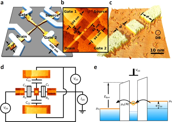
a Electrical contacts (sketched in white) overlaid on top of an STM-patterned SET device. b STM image of the central device region of a typical SET device acquired immediately following hydrogen lithography. The central device region shows a central island that is tunnel coupled with source and drain leads and capacitively coupled to two in-plane gates. Gate 2 is patterned with a deliberate shift towards the source electrode to allow tuning the tunnel coupling symmetry. A high-resolution STM image at the center region is overlaid on a large-scale lower-resolution STM image. c Atomic resolution STM image of an SET pattern where the tunnel gaps are defined with atomic precision. The imaged rows running from upper left to lower right are 2 × 1 surface reconstruction dimer rows on the Si(100) surface. The junction gap separation, d, and junction width, w, are marked in the image. The circle marks the image of a single dangling bond. The STM image is taken at −2 V sample bias and 0.1 nA setpoint current. d An equivalent circuit diagram for the SET, where tunnel junctions are treated as a tunneling resistance and capacitance connected in parallel and the combined coupling of the two gates to the SET island is treated as a capacitor. Gate voltage VGS is applied to both gates in parallel with respect to the grounded source. The drain–source bias VDS is applied to the drain contact lead with respect to the grounded source. e The energy diagram of an SET, where μS and μD are the chemical potentials of the source and drain leads respectively; μIS(N) is the chemical potential of the island that is occupied with N excess electrons. EBarr is 7.
Figure 3 shows a series of STM images acquired following hydrogen lithography with the dimer rows of the surface reconstruction clearly visible. Although not all device drain/source electrodes are aligned to the [110] lattice direction, we observe improved edge uniformity by orienting the device in the [110] lattice direction and aligning the geometries of the critical device region (island and tunnel junctions) with the surface lattice of the reconstruction. For SET-G and SET-I whose tunnel gaps are in the [100] direction, we have corrected for the 45° angle relative to the [110] direction when counting the number of dimer rows in their junction gaps. While attempting to keep lead width and island size identical, we systematically increase the number of dimer row counts within the tunnel junction gap starting from a continuous wire with zero gaps up to SET tunnel gap separations of ~16.2 dimer rows, covering a large range of SET device operation characteristics. Because isolated single dangling bonds do not allow dopants to incorporate, we disregard them in quantifying the device geometry. The critical dimensions after STM-imaging correction are summarized in Table 2 for all devices in this study (see Methods for details). In addition, our regular use of high-resolution STM imaging over the STM-patterned device region allows us to identify atomic-scale defects in the device region, such as step-edges18 and buried charge defects19, which can potentially affect device performance.

a Wire, named Wire-A; b–i single electron transistor (SET) devices, named SET-B to SET-I, corresponding to the panel labels. The drain/source electrodes are oriented in the [110] lattice direction for all cases except for SET-G and SET-I whose drain/source electrodes are oriented in the [100] lattice direction (\(45^ \circ\) to the [110] direction). Different STM tips/tip conditions are used for the STM images under imaging conditions: −2 V sample bias and 0.1 or 0.05 nA setpoint current.
Exponential scaling of tunneling for atomic-scale changes
In Fig. 4a, the current–voltage (I–V) characteristics of Wire-A exhibit Ohmic behavior with a 4-point resistance of 96.8 kΩ. Considering the actual STM-patterned wire geometry (approximately \(57 \pm 4\) squares between the e-beam-patterned voltage contact probes, see Fig. 2a), this corresponds to a sheet resistance of 1.70 ± 0.15 kΩ in the STM-patterned electrodes, in excellent agreement with previous results on metallically doped Si:P delta layers20. Given the ultrahigh carrier density and small Thomas Fermi screening length16 in this saturation-doped Si:P system and the relatively large island size21 of the SETs, we treat the energy spectra in the islands and source and drain leads as continuous (\(\Delta E \ll k_{\mathrm{B}}T\), where \(\Delta E\) is the energy level separation in the island and source and drain reservoirs) and adopt a metallic description of SET transport17. The tunneling rates, \(\Gamma _{\mathrm{{S,D}}}\), and the tunneling resistances, \(R_{\mathrm{{S,D}}} = \hbar /\left( {2\pi e^2\left| A \right|^2D_{\mathrm{i}}D_{\mathrm{f}}} \right)\), across the source and drain tunnel barriers can be described using Fermi’s golden rule22, where A is the tunneling matrix element, \(D_{\mathrm{{i,f}}}\) represents the initial and final density of states, \(\hbar\) is the reduced Plank’s constant, and e is the charge of an electron.

a Four-point \(I_{\mathrm{{DS}}}-V_{\mathrm{{DS}}}\) measurement of the wire device named Wire-A and the single electron transistor (SET) device named SET-B while keeping the gates grounded. Inset: Representative two-point current–voltage (I–V) characteristics (\(3.5\,{\mathrm{k}}{{\Omega }}\)) of a device contact pad. b Differential conductance at zero drain–source bias (\(G_0\)) of the set of SET devices that are measured at T = 4 K. For SET-B to SET-G, \(G_0\) is measured using 0.1 mV alternating current (AC) excitation at 11 Hz. For SET-H and SET-I, \(G_0\) is numerically estimated from the measured direct current (DC) Coulomb diamonds. From top to bottom: SET-B (red) to SET-I (dark blue). The difference in the oscillation period in gate voltage is due to the variations in gate designs that alter the gate capacitance. c The measured total tunneling resistance values \(R_{\mathrm{S}} + R_{\mathrm{D}}\) as a function of the lithographically defined tunnel gap separations. The Wentzel–Kramers–Brillouin (WKB)-fitting is based on the tunneling resistance values from SET-C to SET-I, where the lateral electrical seam width of the electrodes and the mean barrier height are taken as free fitting parameters. d, e The measured differential conductance \({\mathrm{d}}I_{\mathrm{{DS}}}/{\mathrm{d}}V_{\mathrm{{DS}}}\) (on a color linear scale) Coulomb diamonds of SET-C and SET-F, respectively, at T = 4 K.
In the interest of clarity, we define our use of the terms tunnel coupling and tunneling rates. In the context of the work presented here, Eq. (1) relates the tunneling rates to the tunneling resistance values where the tunneling matrix elements, A, represent the tunnel couplings for our system. However, it should be noted that the term “tunnel coupling” is also widely used in the context of quantum dots, where the tunnel coupling is a measure of level broadening of the energy eigenstates on the quantum dots and can lead to a loss of electron localization on the dot in the strong tunnel coupling regime. The term is also used in analog quantum simulation where the tunneling coefficient t in the Hubbard Hamiltonian denotes the hopping energy or tunnel coupling strength between adjacent sites.
In the following, we show that the total tunneling resistance \(R_{\mathrm{S}} + R_{\mathrm{D}}\) of an SET can be extracted by measuring, at zero drain–source direct current (DC)-bias, the peak amplitudes of the differential conductance Coulomb oscillations, as shown in Fig. 4b (see Supplementary Note 1 for typical I–V characteristics of the gates and source/drain leads of STM-patterned SETs). At \(V_{\mathrm{{DS}}} = 0\,{\mathrm{V}}\), the differential conductance Coulomb blockade oscillations reach peaks at \(V_{\mathrm{{GS}}} = V_{\mathrm{{GS}}}^{\mathrm{{peak}}} = \left( {N + \frac{1}{2}} \right)\frac{e}{{C_{\mathrm{G}}}}\), where \(N\) is an integer and \(\left( {N + \frac{1}{2}} \right)e\) represents the effective gating charge when the island Fermi level \(\mu _{\mathrm{{IS}}}(N)\) aligns with \(\mu _{\mathrm{S}}\) and \(\mu _{\mathrm{D}}\). At low temperatures and in the metallic regime, \(\Delta E \ll k_{\mathrm{B}}T \ll E_{\mathrm{C}}\), where \(E_{\mathrm{C}} = e^2/C_{\mathrm{\Sigma }}\) is the charging energy, and \(C_\Sigma = C_{\mathrm{S}} + C_{\mathrm{D}} + C_{\mathrm{G}}\) is the total capacitance (see Supplementary Table 1), and assuming energy independent tunnel rates and density of states in a linear response regime, Beenakker and co-workers23,24 have shown that the peak amplitude of the zero-bias differential conductance oscillations in an SET reduces to the following temperature-independent expression for arbitrary RS and RD values,
where GS and GD are conductances through the source and the drain tunnel barriers, \(\rho\) is the density of state in the metallic island, and the density of states in the leads is embedded in the tunneling rates.
In Fig. 4b we observe Coulomb blockade oscillations in all SETs except SET-B. The small gap separation (~\(7.4\) dimer rows \(\approx 5.7\,{\mathrm{nm}}\)) in SET-B is comparable to twice the Bohr radius, \(r\sim 2.5\,{\mathrm{nm}}\), of an isolated P atom in bulk Si25, indicating significant wave function overlap within the gap regions between the island and the source/drain reservoir. Given that SET-B does not exhibit single electron tunneling behavior (Coulomb oscillations), we estimate the resistance at the junction gaps in this device using 4-point I–V measurement. As shown in Fig. 4a, SET-B has a linear I–V behavior with the 4-point resistance of \(136.7\,{\mathrm{k}}{\Omega}\). Subtracting the resistance contribution from the source/drain leads (~74 squares) using the estimated sheet resistance (~\(1.7\,{\mathrm{k}}{{\Omega }}\)) from Wire-A, we obtain a junction resistance value of \(\sim 5.5 \pm 4.5\,{\mathrm{k}}{{\Omega }}\) per junction in SET-B, which does indeed fall below the resistance quantum (\(\sim {\!}26\,{\mathrm{k}}{{\Omega }}\)), and explains the absence of Coulomb blockade behavior. In SET-B (Fig. 3b), the impact on electrical transport properties that results from having two contacts straddle a single atomic step edge is negligible given the small vertical offset (1 monatomic layer = 0.138 nm) compared with the expected electrical density distribution in the same direction (~2 nm for an ideal, saturation-doped Si:P monolayer)26,27. We emphasize that, due to the absence of the Coulomb blockade effect, the estimated resistance at the junctions in SET-B is an ohmic resistance, which should not be confused with the tunneling resistance.
For the rest of the SETs, we extract the total tunneling resistance, \(R_{\mathrm{S}} + R_{\mathrm{D}}\), from the Coulomb oscillation peak heights following Eq. (1). Figure 4c summarizes the measured junction resistance values (after sheet resistance correction from the source and drain leads) as a function of the averaged gap separations. The tunneling resistance follows a clear exponential relationship with the gap separations. It is notable that a change of only nine dimer rows gives rise to over four orders of magnitude change in the junction resistance. Increasing the gap separation over a small range (from ~7 dimer rows in the gap to ~12) dramatically changes the SET operation from a linear conductance regime (no sign of Coulomb oscillations at ~7 dimer rows separation in SET-B) to a strong tunnel coupling regime (at ~9.5 dimer rows separation in SET-C) to a weak tunnel coupling regime (at ~12 dimer rows separation in SET-F). The relatively strong tunnel coupling in SET-C (see Fig. 4d) blurs the charge quantization on the island and introduces finite conductance within the Coulomb diamonds through higher order tunneling processes (co-tunneling)28. In the weak tunnel coupling regime in SET-F (see Fig. 4e), the Coulomb blockade diamonds become very well established. Tuning the tunnel coupling between strong and weak coupling regimes in atomic devices is an essential capability: e.g. for simulating non-local coupling effects in frustrated systems29.
It has been found essential for capacitance modeling (see Supplementary Table 1) to add a lateral electrical seam30 and a vertical electrical thickness26 to the STM-patterned hydrogen-lithography geometry (Fig. 3) to account for the Bohr radius and yield the actual “electrical geometry” of the device. We fit the total tunneling resistance (\(R_{\mathrm{S}} + R_{\mathrm{D}}\)) from SET-B to SET-H as a function of the tunnel gap separation by simulating a single tunnel junction’s tunneling resistance (multiplied by two to account for the presence of two junctions) using a generalized formula for the tunnel effect based on the Wentzel–Kramers–Brillouin (WKB) approximation31 (for detailed WKB formulation, see Supplementary Note 2: Modeling the Tunnel Barriers Using the WKB Method). Due to the linear dependence of the WKB tunneling resistance on the tunnel junction cross-sectional area, we ignore the small variations in the STM-patterned junction width, \(w\), (see column 3 in Table 2) and adopt an averaged value of \(w = 12\,{\mathrm{nm}}\) in the WKB simulation. We account for the “electrical geometry” of the devices by assuming an electrical thickness of \(z = 2\,{\mathrm{nm}}\)26, while treating the lateral electrical seam width, \(s\), and the mean barrier height, \(E_{\mathrm{{barr}}}\), as fitting parameters. We obtain \(100 \pm 50\,{\mathrm{meV}}\) as the best-fit barrier height (uncertainty represents two σ), which is in good agreement with the theoretically predicted range of Fermi levels below the Si conduction band edge in highly \(\delta\)-doped Si:P systems, ~80 to ~130 meV, from tight-binding26 and density functional theory25 calculations. A similar barrier height value (~80 meV) has also been experimentally determined in a Fowler–Nordheim tunneling regime by Fuhrer’s group using a similar STM-patterned Si:P device8. We obtain \(3.1 \pm 0.4\,{\mathrm{nm}}\) as the best-fit seam width (uncertainty represents two σ), which is in good agreement with the Bohr radius of isolated single phosphorus donors in bulk silicon (\(r\sim 2.5\,{\mathrm{nm}}\))25. Using the best-fit seam width from the WKB simulation, we also find good agreement between the experimental and simulated capacitance values from the SETs (see Supplementary Note 3: Comparison between the Measured and Simulated Capacitances in STM-patterned SET Devices).
Figure 4c is a key result of this study, clearly demonstrating an exponential scaling of tunneling resistance consistent with atomic scale changes in the tunneling gap. The devices shown in Fig. 3 were fabricated in series from two different ultrahigh vacuum (UHV) STM (UHV-STM) systems with similar but non-identical hardware platforms using the same nominal methods and processes.
Atomic-scale asymmetry in precision-patterned SET tunnel gaps
Having demonstrated atom scale control of the tunneling resistance, we now take an additional step to characterize the junction resistance difference in a pair of nominally identical tunnel junctions in SET-G, where both the tunnel gaps have irregular edges and the tunnel gap separations are less well-defined when compared with the tunnel gaps in the other SETs, representing a lower bound of controllability among the SET devices in this study. We present the measured Coulomb diamonds and finite bias Coulomb oscillations in Fig. 5a and b. In Fig. 5b, the Coulomb oscillation peaks are asymmetric across the gate voltage. For positive drain–source bias, at the leading edge of the Coulomb oscillation peak of \(N \leftrightarrow N + 1\) transition, the island spends most of the time unoccupied (\(N\)). So, the total tunneling rate is limited by tunneling from the source to the island, and thus the total tunneling resistance is dominated by \(R_{\mathrm{S}}\). The other three cases are analogous. Figure 5c takes \(V_{\mathrm{{DS}}}\, > \, 0\) for instance and shows a numerical simulation (at \(T = 0\,{\mathrm{K}}\)) of \(I_{\mathrm{{DS}}}\,{\mathrm{{vs}}}.\,V_{\mathrm{{GS}}}\) at different drain–source bias. The dashed and dotted lines in Fig. 5c illustrate the asymptotic slopes at the leading and trailing edges of the Coulomb oscillation peaks at \(V_{\mathrm{{DS}}} = 0.8E_{\mathrm{C}}/e\), which also represent the tunneling current through the rate-limiting source and drain tunnel junctions, respectively, while ignoring the other junction in series. At \(T = 0\,{\mathrm{K}}\), the source and drain junction resistances can be derived from the right derivative at the leading edge, where \(V_{\mathrm{{GS}}} = V_{\mathrm{{GS}}}^{\mathrm{L}} = \left( {N + \frac{1}{2}} \right)\frac{e}{{C_{\mathrm{G}}}} - \frac{{C_{\mathrm{D}}}}{{C_{\mathrm{G}}}}V_{\mathrm{{DS}}}\), and from the left derivative at the trailing edge, where \(V_{\mathrm{{GS}}} = V_{\mathrm{{GS}}}^{\mathrm{T}} = \left( {N + \frac{1}{2}} \right)\frac{e}{{C_{\mathrm{G}}}} + \frac{{(C_{\mathrm{S}} + C_{\mathrm{G}})}}{{C_{\mathrm{G}}}}V_{\mathrm{{DS}}}\), of a Coulomb oscillation peak in \(I_{\mathrm{{DS}}}\). This is shown in Eq. (2) (for mathematical derivations, see Supplementary Note 4: Quantifying Individual Junction Resistances in a Metallic SET), again, taking positive drain–source biases for example,

a The DC-measured Coulomb diamonds, where the drain–source current \(I_{\mathrm{{DS}}}\) is plotted as the absolute values for clarity. b The measured Coulomb blockade oscillations at selected drain–source biases. c Simulated Coulomb blockade oscillations at positive drain–source bias, assuming asymmetric junction resistances \(R_{\mathrm{S}} = 4R_{\mathrm{D}} = 2\,{\mathrm{M}}\Omega\). At \(V_{\mathrm{{DS}}} = 0.8E_{\mathrm{C}}/e\), the dotted and dashed lines plot the simulated tunneling current through the rate-limiting source and drain tunnel junctions at the leading and trailing edges of the Coulomb oscillation peaks, respectively, while ignoring the other junction in series. d The extracted junction resistances from Coulomb oscillation peaks along the gate voltage axis. The horizontal and vertical uncertainties at the data points are calculated by averaging the oscillation peak positions and the tunneling resistances at different drain–source biases.
See Supplementary Table 1 for the gate and total capacitances, \(C_{\mathrm{G}}\) and \(C_\Sigma\). To estimate the drain and source tunneling resistances from the Coulomb oscillation peaks that are measured at finite temperatures (Fig. 5b), we approximate the asymptotic slopes at the leading and trailing edges by fitting the leading and trailing slopes of the measured Coulomb oscillation peaks and average over a range of \(V_{\mathrm{{DS}}}\) bias (see Fig. 5d). We find a factor of approximately four difference in the source and drain tunneling resistances. Possible contributions to this resistance difference include atomic-scale imperfections in the hydrogen lithography of tunnel gaps, the randomness in the dopant incorporation sites within the patterned regions, and unintentional, albeit greatly suppressed, dopant movement at the atomic-scale during encapsulation overgrowth. Field enhancement near any pointed apex due to atomic-scale edge non-uniformity/roughness in the dopant distribution profile can also be an important effect that influences the tunnel current in the Coulomb blockade transport regime, as has been previously suggested by Pascher et al.8. Other factors that can affect the tunnel barrier and therefore cause tunnel resistance variability include changes to the local potential landscape due to buried charge defects near the device region in either the substrate or the overgrowth layer. From the exponential dependence in Fig. 4c, a factor of four corresponds to an uncertainty in the gap separation of only about half of a dimer row pitch distance, which represents the ultimate spatial resolution (a single atomic site on the Si(100)2 × 1 reconstruction surface) and the intrinsic precision limit for the atomically precise hydrogen lithography.
Discussion
The results presented here are of interest where critical device dimensions and pattern fidelity or tunnel coupling play a direct role in device performance. Complex devices such as arrays of quantum dots for analog quantum simulation have stringent requirements with respect to site-to-site tunnel coupling. While the details of the tunneling characteristics are different than an SET in the metallic regime, the fabrication methods described here are applicable to fabrication of single or few atom quantum dots and should aid in achieving a higher degree of reproducibility in those devices32.
In summary, we have demonstrated the ability to reproducibly pattern devices with atomic precision, and that improved locking-layer methods coupled with meticulous control over the entire donor-based device fabrication process resulted in STM patterned devices with predictable tunneling properties. By using the natural surface reconstruction lattice as an atomic ruler, we systematically varied the tunneling gap separations from 7 dimer rows to 16 dimer rows and demonstrated exponential scaling of tunneling resistance consistent with atomic-scale changes in the tunneling gap. We emphasize that, critical fabrication steps, such as a defect- and contaminant-free silicon substrate and hydrogen-resist formation, atomically abrupt and ultra-clean hydrogen lithography, with dopant incorporation, epitaxial overgrowth, and electrical contact formation that suppress dopant movement at the atomic scale, are all necessary to realize devices with atomic precision. This study represents an important step towards fabricating key components needed for high-fidelity silicon quantum circuitry that demands unprecedented precision and reproducibility.
Methods
STM-patterned donor-based device fabrication
The Si:P SETs are fabricated on a hydrogen-terminated Si(100)2 × 1 substrate (\(3 \times 10^{15}\, {\mathrm{cm}}^{ - 3}\) boron doped) in an UHV environment with a base pressure below \(4 \times 10^{ - 9}\,{\mathrm{{Pa}}}\) (\(3 \times 10^{ - 11}\,{\mathrm{Torr}}\)). Detailed sample preparation, UHV sample cleaning, hydrogen-resist formation, and STM tip fabrication and cleaning procedures have been published elsewhere11,18,33. A low 1 × 10⁻¹¹ Torr UHV environment and contamination-free hydrogen-terminated Si surfaces and STM tips are critical to achieving high-stability imaging and hydrogen-lithography operation. The device geometry is defined by selectively removing hydrogen-resist atoms using an STM tip in the low-bias (3–5 V) and high-current (15–50 nA) regime where the small tip-sample separation allows for a spatially focused tunneling electron beam under the atomic-scale tip apex, creating hydrogen lithographic patterns with atomically abrupt edges. For complete hydrogen desorption within the patterned regions, the typical tip scan velocity and scan-line spacing are 100 nm sec−1 and 0.5 nm line−1 respectively. We then saturation-dose the patterned device regions with PH3 followed by a rapid thermal anneal at 350 °C for 1 min to incorporate the P dopant atoms into the Si surface lattice sites while preserving the hydrogen resist to confine dopants within the patterned regions. The device is then epitaxially encapsulated with intrinsic Si by using an optimized locking-layer process to suppress dopant movement at the atomic scale during epitaxial overgrowth12,14. The sample is then removed from the UHV system and Ohmic-contacted with e-beam-defined palladium silicide contacts15.
Low-temperature transport measurements
Low-temperature transport measurements are performed using either a closed-cycle cryostat at a base temperature of 4 K or a dilution refrigerator at a base temperature of ~10 mK. For SET-B to SET-G, the zero-DC bias differential conductance (\({G}_{0}\)) are measured using 0.1 mV AC excitation at 11 Hz. For SET-H and SET-I, \(G_0\) is numerically estimated from the measured DC Coulomb diamonds. We calibrate the zero drain–source bias level by mapping out complete Coulomb diamonds, where the intersections of the Coulomb diamonds represent the true zero-bias condition across the source–drain leads. We extract the zero-bias conductance curves (as shown in Fig. 4) from the measured Coulomb diamond diagrams. Since the effect of gate voltage compensation on the SET island’s chemical potential is insignificant under our measurement conditions at 4 K, we did not compensate \(V_{\mathrm{{GS}}}\) when measuring or calculating \({\mathrm{{d}}}{I}_{\mathrm{{DS}}}/{\mathrm{{d}}}{V}_{{\mathrm{{DS}}}}\) at the zero drain–source bias for extracting the tunnel resistance values. The gate leakage currents are on the order of ~10 pA or less within the gating range used in this study.
Characterization of STM lithographic pattern dimensions
We estimate the critical dimensions of the STM-patterned tunnel junctions in an SET from the STM topography images in Fig. 3, where the gap distance, \(d\), is the average across the full junction width, \(w,\) using both junctions. The junction width is the average over the island and the first 15 nm of the source and drain leads near the island. The hydrogen lithography and STM imaging are carried out using different tips and/or under different tip conditions. To eliminate the STM image-broadening due to the convolution between the wave functions of the tip apex and Si-dangling bonds and extract the boundary of the hydrogen-depassivated surface lattice sites, we estimate the image-broadening, \(\Delta b\), from the difference between the imaged single dangling bond size, \(b\), (full-width at half-maximum) and the size of a single dangling bond lattice site, \(b_0\), where we have assumed \(b_0\) equals half a dimer row pitch (see Fig. 2c). The image-broadening, \(\Delta b = b - b_0\), is then used to correct the critical dimensions that are read out from the half-maximum height positions in the STM topography images.
Theoretical modeling of SETs
The theoretical analysis of the transport through SETs is based on an equivalent circuit model (see Fig. 2d) under a constant interaction approximation. The analytical expressions regarding the equilibrium drain–source conductance are derived using the standard Orthodox theory under a two-state approximation21,34.
Data availability
All relevant data are available upon request from the authors.
References
Hill, C. D. et al. A surface code quantum computer in silicon. Sci. Adv. 1, e1500707 (2015).
Dusko, A., Delgado, A., Saraiva, A. & Koiller, B. Adequacy of Si:P chains as Fermi–Hubbard simulators. npj Quant. Inf. 4, https://doi.org/10.1038/s41534-017-0051-1 (2018).
Koiller, B., Hu, X. & Das Sarma, S. Exchange in silicon-based quantum computer architecture. Phys. Rev. Lett. 88, 027903 (2002).
Wang, Y. et al. Highly tunable exchange in donor qubits in silicon. npj Quant. Inf. 2, https://doi.org/10.1038/npjqi.2016.8 (2016).
Broome, M. A. et al. High-fidelity single-shot singlet-triplet readout of precision-placed donors in silicon. Phys. Rev. Lett. 119, 046802 (2017).
Hanson, R., Kouwenhoven, L. P., Petta, J. R., Tarucha, S. & Vandersypen, L. M. K. Spins in few-electron quantum dots. Rev. Mod. Phys. 79, 1217–1265 (2007).
Pok, W. Atomically Abrupt, Highly-Doped, Coplanar Nanogaps in Silicon. Ph.D. thesis, University of New South Wales (2011).
Pascher, N., Hennel, S., Mueller, S. & Fuhrer, A. Tunnel barrier design in donor nanostructures defined by hydrogen-resist lithography. N. J. Phys. 18, https://doi.org/10.1088/1367-2630/18/8/083001 (2016).
Watson, T. F. et al. Transport in asymmetrically coupled donor-based silicon triple quantum dots. Nano Lett. 14, 1830–1835 (2014).
Shen, T. C. et al. Atomic-scale desorption through electronic and vibrational excitation mechanisms. Science 268, 1590 (1995).
Wyrick, J. et al. Atom-by-atom construction of a cyclic artificial molecule in silicon. Nano Lett. 18, 7502–7508 (2018).
Wang, X. et al. Quantifying atom-scale dopant movement and electrical activation in Si:P monolayers. Nanoscale 10, 4488–4499 (2018).
Hagmann, J. A. et al. High resolution thickness measurements of ultrathin Si:P monolayers using weak localization. Appl. Phys. Lett. 112, 043102 (2018).
Keizer, J. G., Koelling, S., Koenraad, P. M. & Simmons, M. Y. Suppressing segregation in highly phosphorus doped silicon monolayers. ACS Nano 9, 12537–12541 (2015).
Schmucker, S. W. et al. Low-resistance, high-yield electrical contacts to atom scale Si:P devices using palladium silicide. Phys. Rev. Appl. 11, 034071 (2019).
Weber, B. et al. Ohm’s law survives to the atomic scale. Science 335, 64 (2012).
Grabert, H. & Devoret, M. H. eds. Single charge tunneling: Coulomb blockade phenomena in nanostructures (Springer, 1992).
Wang, X., Namboodiri, P., Li, K., Deng, X. & Silver, R. Spatially resolved scanning tunneling spectroscopy of single-layer steps on Si(100) surfaces. Phys. Rev. B 94, 125306 (2016).
Brown, G. W. et al. Imaging charged defects on clean Si(100)-(2×1) with scanning tunneling microscopy. J. Appl. Phys. 92, 820–824 (2002).
Goh, K. E. J., Oberbeck, L., Simmons, M. Y., Hamilton, A. R. & Butcher, M. J. Influence of doping density on electronic transport in degenerate Si:P delta-doped layers. Phys. Rev. B 73, 035401 (2006).
Likharev, K. K. Single-electron devices and their applications. Proc. IEEE 87, 606–632 (1999).
Wasshuber, C. About Single-Electron Devices and Circuits (Technische Univ, Wien, 1997).
Beenakker, C. W. J. Theory of Coulomb-blockade oscillations in the conductance of a quantum dot. Phys. Rev. B 44, 1646–1656 (1991).
Van Houten, H., Beenakker, C. W. J. & Staring, A. A. M. In Single Charge Tunneling: Coulomb Blockade Phenomena in Nanostructures (eds. Grabert, H. & Devoret, M. H.) 167–216 (Springer US, 1992).
Qian, G., Chang, Y.-C. & Tucker, J. R. Theoretical study of phosphorous delta-doped silicon for quantum computing. Phys. Rev. B 71, 045309 (2005).
Carter, D. J., Warschkow, O., Marks, N. A. & McKenzie, D. R. Electronic structure models of phosphorus δ-doped silicon. Phys. Rev. B 79, https://doi.org/10.1103/PhysRevB.79.033204 (2009).
Reusch, T. C. G. et al. Morphology and electrical conduction of Si:P δ-doped layers on vicinal Si(001). J. Appl. Phys. 104, 066104 (2008).
Lee, W. C. T., Scappucci, G., Thompson, D. L. & Simmons, M. Y. Development of a tunable donor quantum dot in silicon. Appl. Phys. Lett. 96, 043116 (2010).
Barthelemy, P. & Vandersypen, L. M. K. Quantum dot systems: a versatile platform for quantum simulations. Ann. Phys. 525, 808–826 (2013).
Weber, B., Mahapatra, S., Watson, T. F. & Simmons, M. Y. Engineering independent electrostatic control of atomic-scale (∼4 nm) silicon double quantum dots. Nano Lett. 12, 4001–4006 (2012).
Simmons, J. G. Generalized formula for the electric tunnel effect between similar electrodes separated by a thin insulating film. J. Appl. Phys. 34, 1793–1803 (1963).
Wyrick, J. et al. Atom-by-atom fabrication of single and few dopant quantum devices. Adv. Funct. Mater. 29, 1903475 (2019).
Deng, X. et al. Silicon epitaxy on H-terminated Si (100) surfaces at 250 °C. Appl. Surf. Sci. 378, 301–307 (2016).
Inokawa, H. & Takahashi, Y. A compact analytical model for asymmetric single-electron tunneling transistors. IEEE Trans. Electron Dev. 50, 455–461 (2003).
Acknowledgements
This work was sponsored by the Innovations in Measurement Science (IMS) program at NIST: Atom-based Devices: single atom transistors to solid-state quantum computing. This work is also funded in part by the Department of Energy Advanced Manufacturing Office Award Number DE‐EE0008311. We thank Neil Zimmerman, Josh Pomeroy, Garnett Bryant, Daniel Walkup, and John Kramar for valuable comments and discussions. This work was performed in part at the Center for Nanoscale Science and Technology NanoFab at NIST.
Author information
Authors and Affiliations
Contributions
X.W. and J.W. conceived of the experiment under the guidance of R.M.S. In situ device fabrication was performed by X.W. and J.W. Ex situ sample preparation and electrical contact fabrication was carried out by P.N., S.W.S, M.D.S. Jr, J.W., and X.W. Low-temperature transport measurement was carried out by R.V.K., A.M., and, X.W. Data analysis and calculations were carried out by X.W., J.W., and R.M.S. The manuscript was prepared by X.W., J.W., and R.M.S. with input from all the authors.
Corresponding author
Ethics declarations
Competing interests
The authors declare no competing interests.
Additional information
Publisher’s note Springer Nature remains neutral with regard to jurisdictional claims in published maps and institutional affiliations.
Supplementary information
Rights and permissions
Open Access This article is licensed under a Creative Commons Attribution 4.0 International License, which permits use, sharing, adaptation, distribution and reproduction in any medium or format, as long as you give appropriate credit to the original author(s) and the source, provide a link to the Creative Commons license, and indicate if changes were made. The images or other third party material in this article are included in the article’s Creative Commons license, unless indicated otherwise in a credit line to the material. If material is not included in the article’s Creative Commons license and your intended use is not permitted by statutory regulation or exceeds the permitted use, you will need to obtain permission directly from the copyright holder. To view a copy of this license, visit http://creativecommons.org/licenses/by/4.0/.
About this article

Cite this article
Wang, X., Wyrick, J., Kashid, R. et al. Atomic-scale control of tunneling in donor-based devices. Commun Phys 3, 82 (2020). https://doi.org/10.1038/s42005-020-0343-1
Received:
Accepted:
Published:
DOI: https://doi.org/10.1038/s42005-020-0343-1
This article is cited by
-
Experimental realization of an extended Fermi-Hubbard model using a 2D lattice of dopant-based quantum dots
Nature Communications (2022)
-
Periodic corner holes on the Si(111)-7×7 surface can trap silver atoms
Nature Communications (2022)
Comments
By submitting a comment you agree to abide by our Terms and Community Guidelines. If you find something abusive or that does not comply with our terms or guidelines please flag it as inappropriate.
