Abstract
This work presents the simulated and measured performance of single- and double-layer frequency selective surface filters for operation at sub-THz frequencies (250 GHz center frequency). They were composed of concentric square loops with a split as a unit cell resonator on top of a low dielectric permittivity, low thickness material (RT5880). Both a single layer filter and a cascaded two layer filter with varied distances were investigated. The simulated bandwidth for the cascaded filter was 27 GHz and 16 GHz and 9 GHz bandwidth measured with a THz-TDS and microwave system.
Introduction
The terahertz band (0.1–10 THz) and especially the sub-THz (0.1–0.3 THz) band are new unallocated radio bands offering new possibilities for future sixth generation (6G) communications, sensing, imaging and joint communication-sensing1,2,3,4,5. Applications in telecommunication, imaging and spectroscopy benefit from the increased bandwidth, small wavelength and high penetrability of non-ionizing radiation3,6,7,8,9. In localization, sensing and imaging applications, the millimeter (mmWave) technologies offer greater accuracy, which promotes the emergence of new applications5,10,11,12,13,14.
For many transceivers it is critical to have good signal-to-noise (SNR) and signal-to-interference-plus-noise ratios (SINR) which can be improved in the THz band with a Frequency Selective Surface (FSS) instead of using a common circuit filter. A FSS filter consists of periodically arranged conductive surfaces having a variety of specific geometries on top of the dielectric surface15. Compared to a common circuit type filter, a FSS filter benefits from lower costs, lower electrical losses and it is more compact in size which allows cheaper and easier prototyping16,17.
FSS technology has been exploited for different applications, such as controllable “smart” surfaces, miniaturized cavity resonators, wave-guide structures, angular-independent surfaces, absorbers, biomedical devices, terahertz switches, fluid-tunable frequency-agile materials, phase modulation, the design of antenna radomes, dichroic surfaces for reflectors and sub-reflectors of large aperture antennas, diplexers, beam splitters and many other applications18,19,20,21,22,23,24,25,26,27,28.
For many applications, the bandwidth of the filter is important and, in the FSS, bandwidth depends on the unit cell and substrate material29. The cascade layers of the FSS have been proposed to be used to increase the operation bandwidth because they lead to a flatter, wider and more stable insertion loss30,31. Misalignment of the cascaded layers has been investigated and found to lead to decreased performance (transmittance and bandwidth)31. The overall frequency response of the FSS layer filter, such as its bandwidth, transfer function and its dependence on the incidence wave angle and polarization, are determined by the grating (inter-element) spacing besides the unit cell parameters30.
The FSS layer typically has grating lobes which are the result of electromagnetic diffraction and spacing between unit cells18. Having a suitable spacing between the unit cells can increase the bandwidth and provide a stable resonance frequency for the filter with respect to the incident angle variations18.
Telecommunication needs Split Ring Resonator (SRR) filters with very wide bandwidths, which cannot easily be met at present. This raises the need to investigate one and two FSS layer bandwidth capability and insertion loss parameters at a particular Sub-THz frequency band (220 GHz to 330 GHz) for the upcoming 6G telecommunication systems.
Previously, a double metamaterial layer resonator with semiconductor (GaAs) material has been studied by tuning the distances of the layers, for THz-TDS with an operation frequency of 0.35 THz32. Also, a similar study has been conducted on a double layer cross frequency selective surface (FSS) unit cell using only metal material (aluminum), fabricated by femtosecond laser machining, for an operating frequency of 0.55 THz33.
In this work, we present a cascaded FSS bandpass filter using low permittivity thin Printed Circuit Board (PCB) operating at 250 GHz. Simulations and design for a single and a double layer FSS using square loop shaped Split Ring Resonators (SRR) are described and analyzed in “Design and simulation of sub-THz bandpass filter” section. In “Experimental results” section, experimental achievements using two different free space measurement methods are presented and discussed. Comparison of the simulations and measurement results are discussed in “Comparison between the simulation and experiments” section. In “Conclusion” section conclusion to this study is offered.
Design and simulation of sub-THz bandpass filter
The firsts step to design the FSS filter was to choose the geometry of the unit cell and the substrate material. Also, an equivalent circuit model of the FSS using lumped elements (L, C, and R) was designed to analyze the frequency resonance of the filter34. Finally, the unit cell matrix (or array) was designed as an FSS layer. A cascaded FSS filter was then formed by placing a second FSS filter on top of the first one with a spacing of 1.5λ.
Circuit model of single unit cell
For this study, a square loop shape SRR was considered with regard to its bandwidth potential and the fact that it has previously been investigated using both analytical expression and a circuit model35,36.
The SRR with an opposing split in the loop was designed for a 250 GHz center frequency on a PCB (RT5880, εr = 2.2)37 using a full wave simulator (CST)38. The schematic of the SRR is shown in Fig. 1a and parameters for the unit cell are listed in Table 1. An equivalent circuit model of the SRR for Transverse Electro Magnetic waves (TEM) mode with respective symbols for capacitance C, inductance L and gap in the ring Cgap where index 1 represents the outer ring and index 2 the inner ring is shown in Fig. 1b. Between the rings there is mutual magnetic coupling M which happens due the metal also acts as a coil and its magnetic field couples between the coils. Simulated magnetic and electric fields are in Fig. 1c,d. The H-field was coupled in the y-direction and E-field in the x-direction when the plane wave passed through the SRR in the z-direction.
(a) Schematic of the single SRR (values are presented in the Table 1), (b) equivalent circuit model of the SRR for TEM mode, (c) Simulated magnetic field was coupled in the y-direction and (d) Simulated electric field was coupled in the x-direction.
Modeling of two cascaded unit cells
Two-unit cells were placed at a distance of 900 µm from each other and their simulated electric and magnetic field amplitudes are presented in Fig. 2. A plane wave traveled through the layers as in the single layer case and E- and H-fields are presented in Fig. 2a,b. Having a cascaded structure did not alter the fields’ coupling directions, it only changed the field strengths; E-field (from 8.8 × 10⁵ to 1.6 × 10⁶ V/m) and H-field (1357 to1589 A/m).
Simulated S-parameters, insertion loss (S21) and reflection coefficient (S21) for Transverse Electric wave (TE) and Transverse Magnetic wave (TM) modes for the broad band 230–280 GHz for single and two-layer with three spacings were investigated and results are shown in Fig. 3. For TE mode, a single unit cell performed with a lower than − 10 dB reflection coefficient (S11) from 237 to 265 GHz and with insertion losses (S21) approximately 0.1 dB. The two-layer FSS, showed a − 10 dB reflection coefficient with insertion losses around 0.12 dB at 242 GHz to 272 GHz. There was a second resonance presented with 1.267 mm and 1.367 mm distances at frequencies 265 GHz and 278 GHz, respectively. Cascading the unit cells mutual coupling impacted the S11 scattering parameter. On increasing the spacing between layers, the bandwidth of the SRR filter decreased, and vice versa. As seen in Fig. 3b, the S11 with a spacing of 1.267 mm showed more mutual coupling than at 1.367 mm spacing and the bandwidth was wider. For TM mode, the frequency has been shifted to 272 GHz showing around − 20 dB reflection losses at all but the 1.367-layer distance, S11 was − 50 dB and insertions losses for all cases were near 0 dB. Furthermore, the impact of the second layer on the simulated phase is seen in Fig. 4 and it shows some phase deviation between one and two-layer SRR filters at both modes.
Parameters regarding the FSS bandwidth, S parameters, reflection coefficient, insertion loss, phase and distance for the TE mode are shown in Table 2. Changing the spacing between two layers can impact operation parameters including bandwidth (BW) and insertion loss and phase difference. For example, by increasing the spacing the bandwidth became wider, 27 GHz, but insertion loss was increased as well. On the other hand, reducing spacing (1267 mm, optimized structure), the bandwidth decreased to 18 GHz, but insertion loss reduced. By decreasing the spacing between the layers even further, the BW decreased to 15 GHz with no visible changes in the insertion loss.
Full array modeling analysis
The full array was modelled with 32 × 30 elements on a planar lattice with an inter element distance of λ/2 and a TE mode planewave illuminating the filter from the rear side. An electric probe was placed in front of the FSS to measure the electric field strength after it had passed through the FSS. The periodic lattice caused phenomena e.g., surface wave, surface impedance and mutual impedance, besides the resonant phenomena. Interelement spacing could control unwanted grating lobes, which had the potential to degrade the performance. Inter element distances were simulated for three distances and results are shown in Fig. 5. Decreasing the distance, the bandwidth was decreased, and vice versa.
Experimental results
In this section, the FSS filter was fabricated, and its electrical performance was measured using two different methods, THz time-domain spectroscopy (THz-TDS) and microwave systems. THz-TDS was used to measure transmittance and time delay and the microwave system was used to measure the S-parameters.
Fabrication of FSS filter layer
The FSS filter was fabricated using low permittivity material (RT5880, ε = 2.2) and a photolithography method and its picture is shown in Fig. 6. The fabricated FSS layer was composed of 960-unit cells, Fig. 6, (a) left side and the picture of a square loop SRR, right side Fig. 6b. The close up image shows some additional erosion which came from the lithography method, as expected.
Measurement using THz time-domain spectroscopy
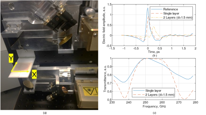
A TeraPulse system (TeraPulse 4000, Teraview UK)39, Fig. 7a, was used to measure the FSS filter’s impact on time-delay and transmittance and the results are shown in Fig. 7b,c. The single layer FSS filter was placed between two mirrors and the thickness of the FSS created a time-delay (around 0.1 picosecond) and reduced the amplitude to 0.9 compared to the reference signal amplitude (12.5). With a second layer, the time-delay increased to 0.5 ps and reduced the transmittance amplitude to 0.43. It was observed that each layer reduced the transmitted wave amplitude by around 30%. The bandwidth was measured to be ~ 12 GHz with one layer and ~ 16 GHz with two layers at 95% transmittance level.
Measurement set up using microwave system
A microwave measurement system consisting of a PNA (operation frequency 67 GHz) and a pair of VDI extenders (Tx and Rx with operation frequency from 220 to 330 GHz) was used to measure the S-parameters, as shown in Fig. 8a. The Tx was connected to a rectangular waveguide (WR3.4) and a standard horn antenna (TE mode) was connected to the Rx. The FSS filter was located in the middle of the beam and the measured S-parameters are shown in Fig. 8b. The results show insertion losses with and without smoothing, solid and dashed line. Measured insertion losses for both cases at 250 GHz were ~ 3 dB. Bandwith for a single layer was ~ 7 GHz and for a double layer it was 9 GHz.
Comparison between the simulation and experiments
The FSS simulation, THz-TDS, and microwave measurements normalized results are presented in Fig. 9. Simulations were done using a Floquet mode simulation which used either a TE or TM planewave as a propagating wave, the THz-TDS use the focused pulse propagating in free space and the microwave system a wave guide and a horn antenna (both TE mode antennas).
For a single layer, the simulation bandwidth was around 20 GHz, 10 GHz for THz-TDS and 7 GHz for the microwave system. For two layers, the simulation bandwidth was around 27 GHz, 16 GHz for THz-TDS and 9 GHz for the microwave system. Simulation for the single layer case showed a wider bandwidth compared to the THz-TDS and microwave system. In the microwave results, grating lobes are clearly visible in the single- and double-layer cases. Despite the differences in the simulations and measurements, they all conclude the same thing, a cascaded FSS filter on a PCB does work in both simulations and measurements in the Sub-THz frequency band.
Conclusion
This work presented an FSS filter consisting of SRR’s on PCB (RT5880) for a 250 GHz center frequency. The FSS layer was designed with a full wave simulation for TE mode and it was predicted to have 27 GHz bandwidth when two FSS layers were at a distance of 1.367 mm from each other. It was noted that changing the layers’ distance impacted on the bandwidth. On increasing the spacing the bandwidth was decreased and vice versa. This allows another way to control the bandwidth as only the distance of the layers needs to be changed. Also, the inter element spacing impacted on the bandwidth; having too large a spacing caused the bandwidth to decrease. Additionally, phase was impacted by a second layer as well. At 250 GHz a 27 degree shift from a single layer level was observed.
The filter was fabricated on RT5880 using a lithography method and the resulting filter had 32 × 30 unit cells on an area ~ 3 × 3 cm2. The cascaded filter was measured with THz-TDS and a microwave system and the measured bandwidth was 16 GHz and 9 GHz, respectively. Additionally, in the THz-TDS measurements a time delay and signal transmission was analyzed. The time delay was 0.1 ps and 0.5 ps and transmission 0.9 and 0.43 for single and double layer, respectively. Variations between the results have been considered to come from different wave shapes, beam widths and different measurement system geometries. Cascaded filters could be one of the potential solutions to increase the filter bandwidth in the future.
Data availability
The data that support the findings of this study are available from the corresponding author, A. G, upon reasonable request.
References
Matinmikko-Blue, M., Yrjölä, S. & Ahokangas, P. Moving from 5G in verticals to sustainable 6G: Business, regulatory and technical research prospects. In Cognitive Radio-Oriented Wireless Networks (eds Caso, G. et al.) 176–191 (Springer International Publishing, 2021). https://doi.org/10.1007/978-3-030-73423-7_13.
Zhang, Z. et al. 6G wireless networks: Vision, requirements, architecture, and key technologies. IEEE Veh. Technol. Mag. 14, 28–41 (2019).
Rappaport, T. S. et al. Wireless communications and applications above 100 GHz: Opportunities and challenges for 6G and beyond. IEEE Access 7, 78729–78757 (2019).
Wild, T., Braun, V. & Viswanathan, H. Joint design of communication and sensing for beyond 5G and 6G systems. IEEE Access 9, 30845–30857 (2021).
Božanić, M. & Sinha, S. 6G networks: Fusion of communications, sensing, imaging, localization and other verticals. In Mobile Communication Networks: 5G and a Vision of 6G (eds Božanić, M. & Sinha, S.) 305–335 (Springer International Publishing, 2021).
Chen, Z. et al. A survey on terahertz communications. China Commun. 16, 1–35 (2019).
T. Kürner, D. Mittleman, and T. Nagatsuma, Eds., THz Communications: Paving the Way Towards Wireless Tbps. Springer International Publishing, (2021). https://doi.org/10.1007/978-3-030-73738-2.
Mittleman, D. M. Twenty years of terahertz imaging [Invited]. Opt. Express 26, 9417–9431 (2018).
Uusitalo, M. A. et al. Hexa-X The European 6G flagship project. in 2021 Joint European Conference on Networks and Communications 6G Summit (EuCNC/6G Summit) 580–585 (2021). https://doi.org/10.1109/EuCNC/6GSummit51104.2021.9482430.
Jackson, J. B. et al. A survey of terahertz applications in cultural heritage conservation science. IEEE Trans. Terahertz Sci. Technol. 1, 220–231 (2011).
Ghavidel, A. et al. A sensing demonstration of a sub THz radio link incorporating a lens antenna. Prog. Electromagn. Res. Lett. 99, 119–126 (2021).
Beruete, M. & Jáuregui-López, I. Terahertz sensing based on metasurfaces. Adv. Opt. Mater. 8, 1900721 (2020).
Hillger, P., Grzyb, J., Jain, R. & Pfeiffer, U. R. Terahertz imaging and sensing applications with silicon-based technologies. IEEE Trans. Terahertz Sci. Technol. 9, 1–19 (2019).
Kokkonen, M., Juttula, H., Mäkynen, A., Myllymäki, S. & Jantunen, H. The effect of drop shape, sensing volume and raindrop size statistics to the scattered field on 300 GHz. IEEE Access 9, 101381–101389 (2021).
Panwar, R. & Lee, J. R. Progress in frequency selective surface-based smart electromagnetic structures: A critical review. Aerosp. Sci. Technol. 66, 216–234 (2017).
Quevedo-Teruel, O. et al. Roadmap on metasurfaces. J. Opt. U. K. 21, 073002 (2019).
Bukhari, S. S., Vardaxoglou, J. & Whittow, W. A metasurfaces review: Definitions and applications. Appl. Sci. Switz. 9, 2727 (2019).
Wang, D. S., Qu, S.-W. & Chan, C. H. Frequency selective surfaces. In Handbook of Antenna Technologies (eds Chen, Z. N. et al.) 471–525 (Springer Singapore, 2016). https://doi.org/10.1007/978-981-4560-44-3_23.
Holloway, C. L. et al. An overview of the theory and applications of metasurfaces: The two-dimensional equivalents of metamaterials. IEEE Antennas Propag. Mag. https://doi.org/10.1109/MAP.2012.6230714 (2012).
Landy, N. I., Sajuyigbe, S., Mock, J. J., Smith, D. R. & Padilla, W. J. Perfect metamaterial absorber. Phys. Rev. Lett. 100, 207402 (2008).
Lee, S.-W. Scattering by dielectric-loaded screen. IEEE Trans. Antennas Propag. 19, 656–665 (1971).
Yuan, Y. et al. Independent phase modulation for quadruplex polarization channels enabled by chirality-assisted geometric-phase metasurfaces. Nat. Commun. 11, 4186 (2020).
Zhang, K. et al. Polarization-engineered noninterleaved metasurface for integer and fractional orbital angular momentum multiplexing. Laser Photonics Rev. 15, 2000351 (2021).
Yuan, Y. et al. Complementary transmissive ultra-thin meta-deflectors for broadband polarization-independent refractions in the microwave region. Photonics Res. 7, 80–88 (2019).
Mahmoodi, M., VanZant, L. & Donnell, K. M. An aperture efficiency approach for optimization of FSS-based sensor resolution. IEEE Trans. Instrum. Meas. 69, 7837–7845 (2020).
Myllymäki, S. & Kokkonen, M. 240 GHz meta-surface band pass filter and lens integration in 6G telecommunication systems. Microw. Opt. Technol. Lett. 63, 2013–2017 (2021).
Munk, B. A. Frequency Selective Surfaces: Theory and Design (Wiley-Interscience, 2000).
Kehn, M. N. M., Rajo-Iglesias, E. & Quevedo-Teruel, O. Parametric study of dispersion and filtering capabilities of SRR-type FSS loaded rectangular waveguides. in 2007 IEEE Antennas and Propagation Society International Symposium 2365–2368 (2007). https://doi.org/10.1109/APS.2007.4396007.
Yang, F., & Rahmat-Samii, Y. (Eds.). Surface Electromagnetics: With Applications in Antenna, Microwave, and Optical Engineering. Cambridge: (Cambridge University Press, 2019). https://doi.org/10.1017/9781108470261
Sarabandi, K. & Behdad, N. A frequency selective surface with miniaturized elements. IEEE Trans. Antennas Propag. 55, 1239–1245 (2007).
Ri-Hui, X. & Jiu-Sheng, L. Double-layer frequency selective surface for terahertz bandpass filter. J. Infrared Millim. Terahertz Waves 39, 1039–1046 (2018).
Reiten, M. T. et al. Resonance tuning behavior in closely spaced inhomogeneous bilayer metamaterials. Appl. Phys. Lett. 98, 131105 (2011).
Gao, T. et al. Resonant coupling effects in a double-layer THz bandpass filter. Appl. Sci. 10, 5030 (2020).
Rahmat-Samii, Y. & Mosallaei, H. Electromagnetic band-gap structures: classification, characterization, and applications. in 2001 Eleventh International Conference on Antennas and Propagation, (IEE Conference Publication No. 480) vol. 2 560–564 (2001).
Saha, C. & Siddiqui, J. Y. A comparative analyis for split ring resonators of different geometrical shapes. in 2011 IEEE Applied Electromagnetics Conference (AEMC) 1–4 (2011). https://doi.org/10.1109/AEMC.2011.6256871.
Anwar, R. S., Mao, L. & Ning, H. Frequency selective surfaces: A review. Appl. Sci. 8, 1689 (2018).
RT/duroid® 5880 Laminates—Rogers Corporation. https://rogerscorp.com/advanced-electronics-solutions/rt-duroid-laminates/rt-duroid-5880-laminates
CST Studio Suite 3D EM simulation and analysis software. https://www.3ds.com/products-services/simulia/products/cst-studio-suite/
World Leading Terahertz Solutions. TeraView https://teraview.com/
Acknowledgements
This work has been funded partly by Microelectronics Research Unit, University of Oulu and partly by Academy of Finland 6Gensis flagship (Grant No. 318927).
Author information
Authors and Affiliations
Contributions
Idea A.G., simulations A.G. and M.K., measurements A.G. and S.M., writing, reviewing, editing, polishing and approving the final version all authors.
Corresponding author
Ethics declarations
Competing interests
The authors declare no competing interests.
Additional information
Publisher's note
Springer Nature remains neutral with regard to jurisdictional claims in published maps and institutional affiliations.
Rights and permissions
Open Access This article is licensed under a Creative Commons Attribution 4.0 International License, which permits use, sharing, adaptation, distribution and reproduction in any medium or format, as long as you give appropriate credit to the original author(s) and the source, provide a link to the Creative Commons licence, and indicate if changes were made. The images or other third party material in this article are included in the article's Creative Commons licence, unless indicated otherwise in a credit line to the material. If material is not included in the article's Creative Commons licence and your intended use is not permitted by statutory regulation or exceeds the permitted use, you will need to obtain permission directly from the copyright holder. To view a copy of this licence, visit http://creativecommons.org/licenses/by/4.0/.
About this article
Cite this article
Ghavidel, A., Kokkonen, M. & Myllymäki, S. A double layer FSS filter for sub-THz applications. Sci Rep 11, 19773 (2021). https://doi.org/10.1038/s41598-021-99256-2
Received:
Accepted:
Published:
DOI: https://doi.org/10.1038/s41598-021-99256-2
This article is cited by
Comments
By submitting a comment you agree to abide by our Terms and Community Guidelines. If you find something abusive or that does not comply with our terms or guidelines please flag it as inappropriate.


