
Abstract
Biological research and diagnostic applications normally require analysis of trace analytes in biofluids. Although considerable advancements have been made in developing precise molecular assays, the trade-off between sensitivity and ability to resist non-specific adsorption remains a challenge. Here, we describe the implementation of a testing platform based on a molecular-electromechanical system (MolEMS) immobilized on graphene field-effect transistors. A MolEMS is a self-assembled DNA nanostructure, containing a stiff tetrahedral base and a flexible single-stranded DNA cantilever. Electromechanical actuation of the cantilever modulates sensing events close to the transistor channel, improving signal-transduction efficiency, while the stiff base prevents non-specific adsorption of background molecules present in biofluids. A MolEMS realizes unamplified detection of proteins, ions, small molecules and nucleic acids within minutes and has a limit of detection of several copies in 100 μl of testing solution, offering an assay methodology with wide-ranging applications. In this protocol, we provide step-by-step procedures for MolEMS design and assemblage, sensor manufacture and operation of a MolEMS in several applications. We also describe adaptations to construct a portable detection platform. It takes ~18 h to construct the device and ~4 min to finish the testing from sample addition to result.
Introduction
Detection of trace analytes or biomarkers in complex biofluids (down to 1–10 copies in 100 μl) is of great importance in fields such as biological research, precision medicine and early-stage diagnosis1,2,3,4. Until now, diverse sensing technologies have been studied; these include spectroscopy5,6, magnetic resonance imaging7,8, chromatography9,10, ion mobility spectrometry11,12, immunoassay13,14,15,16, PCR17,18, electrochemiluminescence19,20, surface-enhanced Raman spectroscopy21,22, surface plasmon resonance (SPR)23,24, and electrochemical sensors4,25, which have been developed for research and commercial applications. Although these technologies have achieved great progress, they suffer from insufficient sensitivity when detecting trace analytes in unamplified samples. To enhance the signal, analyte enrichment or amplification such as amplification of low amounts of nucleic acid by PCR is usually required26,27, which necessitates complicated preparation and increases testing time. More importantly, there is a trade-off between sensitivity and antifouling capability of preventing non-specific adsorption28. Non-specific adsorption of proteins, nucleic acids or other background molecules in biofluids may increase background noise, block receptor active sites and compromise the sensitivity of the assay. In addition, these technologies require costly instruments, usage of labels and well-trained operators and are not portable. These limitations are difficult to mitigate, partially because of a lack of strategy for actively manipulating sensing operations at the molecular level. In contrast, bio-recognition and specific response with remarkable precision happen in living systems. These sensing behaviors are dependent on precisely regulated molecular mechanisms such as protein synthesis29, metabolism30 and transmembrane signaling31, providing an alternative way to design artificial sensing systems operating in biofluids and overcome the aforementioned limitations.
Microelectromechanical systems (MEMSs) and nanoelectromechanical systems (NEMSs) integrate electrical and mechanical components at the microscale and nanoscale dimensions, respectively, to convert mechanical, chemical, biological or other sensing responses to electrical signals. From 196732, researchers started to combine the MEMS/NEMS technology with field-effect transistors (FETs). Recent studies show that by integration with FETs, sensitive MEMS/NEMS biosensors can be achieved because of efficient signal transduction resulting from external perturbation and the inherent capability of signal amplification of FETs33,34,35,36,37. Nevertheless, the precision is still far below that of living systems. Smaller dimensions of the sensing component mean higher sensitivity because a smaller sensing component undergoes a larger change in physical properties when subjected to external perturbations. Without designing and manipulating the systems at the molecular level, the limit of detection (LoD) of MEMSs/NEMSs and FETs rarely reaches 10−17 M (~600 copies in 100 μl) in buffer or diluted biofluid28,33,34,35,38,39,40,41,42,43,44. The sensitivity is lower in complex and high-ionic-strength biofluids, meaning these systems do not meet the requirements for precise detection and diagnosis.
In this protocol, we describe a testing platform based on a molecular-electromechanical system (MolEMS) that is manufactured and actuated with molecular-scale precision, permitting detection of trace analytes in complex biofluids. By using a graphene FET (g-FET) equipped with a MolEMS, unamplified detection of thrombin, Hg2+, ATP and severe acute respiratory syndrome coronavirus 2 (SARS-CoV-2) nucleic acids has been achieved with an LoD of several copies/molecules in 100-μl buffer, serum or nasopharyngeal swab samples45. The applicability to different kinds of analytes holds promise in wide-ranging applications such as rapid pathogen screening, disease diagnosis, health monitoring and food and environmental safety.
Development of the protocol
FET biosensor
An FET is an elementary unit in solid-state electronics. It typically consists of a semiconductor channel with electrodes at either end referred to as the ‘drain’ and the ‘source’. A gate electrode is placed in very close proximity to the channel through a dielectric layer. By applying a potential across the dielectric layer, an electric field modulates the conductivity of the semiconductor and controls the current flowing through the channel. Because of their inherent capability of signal amplification, FETs have emerged as candidates for sensitive bio-detection, with advantages such as fast response, label-free detection, easy integration of multiple devices for high throughput, user friendliness and suitability for point-of-care testing46.
An FET biosensor is usually configured as a liquid-gated FET (Fig. 1), where desired probes are functionalized on the surface of the channel. When exposed to an aqueous environment, an electrical double layer formed at the interface between the electrolyte solution and the channel serves as the dielectric layer47. Once charged biomolecules bind to the probes, a change in surface potential is induced, thereby altering the charge dispersal of the underlying semiconductor material. This results in a change in conductance of the FET channel, transducing the biochemical signal to electrical signal in a real-time, specific and label-free manner39,41,48,49,50,51,52,53,54.

Probes are functionalized on the semiconducting channel. Recognition of analyte by probes induces a change in conductivity of the channel. The probe could be an antibody, single-stranded DNA (ssDNA; or aptamer), enzyme, CRISPR–Cas, etc. The analytes include proteins, nucleic acids, ions, organics and pathogens.
Challenges
Given the complexity of biological samples, sensitive detection of trace analytes in biofluids requires a carefully designed sensing interface. In particular, the sensing interface of the FET must have the ability to (i) recognize the analytes with high efficiency, (ii) resist non-specific adsorption, and (iii) overcome the Debye length limitation in high-ionic-strength biofluids. In biological detection, the Debye length may limit detection because analyte recognition events beyond this length from the FET surface are shielded by ions in solution55. Although successful efforts toward developing FET sensors that fulfil these individual features have been reported4,35,56, it is difficult to simultaneously satisfy the above requirements with the existing FET sensors. To solve this problem, the key challenge is to successfully manipulate sensing processes to achieve all the aforementioned capabilities.
DNA nanostructures in bio-detection
Single-stranded DNA (ssDNA) aptamer probes have received considerable attention because of their high specificity, affinity, stability, synthetic availability and batch-to-batch uniformity57. Thus, ssDNA probes targeting a wide range of analytes have been extensively used in FET biosensors33,58,59,60. Furthermore, the intrinsic lock-and-key assembly mechanisms61,62 and the mass commercial synthesis of nucleic acid have led to rapid progress in DNA nanotechnology over recent decades63,64. DNA sequence can be designed to construct desired conformation structures, allowing the development of different sensing mechanisms for various scenarios65,66. In particular, nucleic acid sequence can be manipulated to construct numerous DNA nanostructures with a designed configuration and dimensions via a one-step self-assemblage mechanism. DNA nanostructures serving as probe carriers enable precise spatial arrangement of biomolecules with a theoretic resolution of a single nucleotide, permitting manipulation of sensing events with molecular precision67. The high programmability of 2D and 3D DNA nanostructures has leveraged many artificial biological systems such as molecular machines68, molecular reactors69 and molecular carriers70. These DNA nanostructure-constructed systems help to not only understand fundamental mechanisms of biological processes but also manufacture functional systems including biosensors with higher precision.
From a MEMS/NEMS to a MolEMS
MEMSs/NEMSs, the miniaturized functional systems integrating electrical and mechanical components at micrometer or nanometer scale, function as an interface between microelectronic or nanoelectronic components and the environment. The micrometer- and nanometer-length scales are particularly relevant to biological materials because these scales are comparable to the size of cells, diffusion lengths of molecules and electrostatic screening lengths of ion-conducting fluids. Hence, the applications of MEMS and NEMS in bio-detection have expanded over the past decades, evolving from MEMS-based methods such as quartz crystal microbalance sensors, microfluidic sensor chips and cantilevers to NEMS-based methods such as nano-resonators71,72,73,74,75,76,77,78. By integration with FETs, MEMSs/NEMSs can be used as sensitive biosensors, because FETs combine efficient transducers with signal amplifiers in which a small parameter alteration induces a pronounced change in channel current. It has been demonstrated that the miniaturized feature size of MEMSs/NEMSs significantly improves sensing performance while reducing cost, volume, weight and power consumption79,80,81. In considering this point, further decreasing the feature size is highly desired.
Inspired by highly precise structure and versatile functions offered by DNA nanostructures, we describe a recently developed electromechanical system, named ‘MolEMS’, which reduces the feature size down to the molecular scale and resolves many of the challenges of FETs to allow for rapid detection of trace analytes in biofluids45. The MolEMS is a self-assembled DNA nanostructure containing a stiff tetrahedral double-stranded DNA (dsDNA) base and a flexible ssDNA cantilever with a probe on the tip (Fig. 2a). The base is immobilized on the channel of a liquid-gated g-FET. A severe charge screening effect exists in high-ionic-strength solutions, such as serum or blood, leading to low sensitivity of direct detection of analytes in the physiological environment. Upon electromechanical actuation by applying a negative gate voltage (Vg) on the g-FET (Fig. 2b), the cantilever can be electromechanically actuated downward, modulating sensing events close to the graphene channel. Thus, the MolEMS g-FET overcomes the Debye length limitation (Fig. 2e), permitting efficient signal transduction. Meanwhile, the high-density stiff tetrahedral bases functionalized on the channel (Fig. 2c,d) serve as a built-in antifouling layer, preventing non-specific adsorption to graphene. By manipulating the sensing operation at a molecular scale not achieved by other traditional FET sensors, the detection of trace analytes can be realized in complex biofluids such as serum and could be expanded to blood, urine and saliva.

a, Sensor components of a MolEMS that resemble a cantilever system including a rigid tetrahedral double-stranded DNA (dsDNA) base and a flexible ssDNA probe. b, Configuration of a MolEMS g-FET. The MolEMS is immobilized on the channel surface of a liquid-gated g-FET, with an Ag/AgCl electrode serving as the gate electrode. c, Optical microscope image of the graphene channel. Scale bar, 100 μm. d, Atomic force microscopy image of the MolEMS immobilized on the graphene surface. The image was obtained in 1× Tris-magnesium sulfate (1× TM) buffer. The color bar indicates the height. Scale bar, 100 nm. The measured size is consistent with the theoretical dimensions of the MolEMS. e, The working principle of the MolEMS. At a negative gate voltage (Vg), analytes recognized by the ssDNA probes (i) are actuated to the graphene surface within the Debye length (ii), while the rigid tetrahedral dsDNA bases functionalized on the graphene surface function as an antifouling layer to resist non-specific adsorption of background molecules in biofluids (iii). Panels c and d adapted from ref. 45, Springer Nature Ltd.
Comparison with other methods
Because they are affected by orders-of-magnitude higher amounts of background biomolecules or inefficient signal transduction, mainstream clinical assay approaches such as ELISA and other immunoassay approaches might be incapable of achieving an LoD of ~10−13 M82,83,84,85,86,87,88, which is required for trace analyte detection in some biological research and diagnostic applications. To overcome this challenge, analyte enrichment or amplification strategies have been used. For example, gold or magnetic nanoparticles are used to pre-concentrate analytes so that the signal can be enhanced89,90,91. Nucleic acids need be amplified by PCR17,18, loop-mediated isothermal amplification92,93,94 or recombinase polymerase amplification95,96 before measurement. However, these strategies inevitably complicate the sensing process and are time consuming. Although rapid testing methodologies based on colorimetric assays97,98, electrochemical assays4,25,99, SPR23,24 and CRISPR100,101,102 have been extensively investigated, unfortunately, the LoD rarely reaches 10−17 M in bulk buffer or diluted biofluids28,33,34,35,38,39,40,41,42,43,44 (Table 1). Although techniques using nanometer-sized transducers have been developed to monitor one or a few molecules, these methods require exquisite micro- and nano-fabrication to obtain nano-scaled recognition cross-sections3,103, which limits the scale of their application.
As an alternative, the FET sensor emerges as a candidate for trace analyte detection because of the inherent signal amplification and rapid response. Nevertheless, detecting analytes in physiological conditions by FETs is hindered by the small Debye length and non-specific adsorption of biomolecules. Researchers have developed several strategies to address the Debye length issue. By crumpling the conducting channel or reducing receptor size, the binding events have been brought to the immediate vicinity of the channel surface51,104,105. Although these approaches have been proven to enhance signal transduction, they do not achieve universal, active and precise controlling of sensing operations. To overcome non-specific adsorption, strategies such as directly coating the surface with antifouling chemicals or porous membranes have been developed28,106. These strategies complicate either the sensing interface design or testing procedure. In considering the Debye length in physiological conditions, coating of the antifouling layer inevitably places the sensing events further beyond the Debye length55, which hinders signal transduction of FETs. Therefore, the trade-off between the above-mentioned limitations so far has not been successfully addressed.
In contrast, the electrostatic actuation of a MolEMS on FETs precisely manipulates the sensing process at the molecular scale and overcomes the Debye length limitation, while the in-built antifouling capability simultaneously resists non-specific adsorption, enabling unamplified detection of trace analytes in biofluids. For example, nucleic acid testing by PCR needs time-consuming purification and amplification processes, and the LoD is typically ~200–1,000 copies ml−1 (~0.3 × 10⁻¹⁸–1.7 × 10⁻¹⁸ M) even after amplification by more than 106-fold92,107,108,109. MolEMS g-FETs directly detect nucleic acids in biofluids with an LoD of ~10–20 copies ml−1. This sensitivity remains even after 15 days of continuous exposure to undiluted serum.
Advantages and applications
A MolEMS is a miniaturized electromechanical system that can be used to manipulate sensing processes with molecular precision. By coupling a MolEMS on the FET surface, efficient signal transduction enables direct detection of trace analytes in complex biofluids without analyte enrichment or amplification, which is difficult to achieve by conventional testing technologies. The label-free and one-step electric readout of a MolEMS g-FET significantly improves the testing efficiency. In addition, an FET is amenable to miniaturization, which improves its portability and allows point-of-care testing applications. Multiple sensing units can be integrated on a single testing module so that various analytes can be simultaneously tested110, allowing multiple testing scenarios to be achieved with reduced cost. Moreover, the automation of FET-based testing provides the merit of easy operation, removing the requirement for skilled personnel.
Importantly, by replacing the cantilever with target ssDNA probes, MolEMSs have been applied to assay different analytes including ions, small molecules, proteins and nucleic acids45. In this protocol, we demonstrate electromechanical detection of thrombin, ATP, Hg2+ and nucleic acids (cDNA and RNA). In a clinical application, MolEMS g-FETs are used for the first time for detection of SARS-CoV-2 RNA in unamplified samples within 4 min, promising on-site and point-of-care pathogen testing outside of laboratories, such as in airports, clinics and even at home. This technology has the potential to be a comprehensive assay platform in wide-ranging applications such as rapid pathogen screening, disease diagnoses, health monitoring, environmental safety and others.
Limitations
Although the effectiveness and universality of MolEMS-based analyte testing have been proven in the laboratory in both buffer and serum, for real-world use, further optimization of the design of the signal amplifier and operating conditions is required. In particular, the device-to-device deviation in output performance of MolEMS g-FETs affects the results of analyte testing. The difference in transconductance leads to variation in electrical response, thereby hindering the application of this system in precise analyte quantification. Such deviations possibly come from MolEMS synthesis, g-FET device fabrication or MolEMS functionalization on g-FETs. To mitigate these deviations, standardization of these technical processes needs to be established at industrial scale to enable practical applications of MolEMSs in clinical assays or pathogen screening.
The MolEMS technique described in this protocol focuses on analyte detection. Applications beyond this area have not been explored. For example, the MolEMS technique could help to build other artificial electromechanical devices and functional systems for chemical and biological applications111 with higher precision and more functionalities than conventional technologies. Future efforts in this area could not only validate the universality of the MolEMS technique but also greatly expand its applications.
Experimental design
MolEMS design
To achieve sensitive analyte detection in biofluids, the design of the MolEMS structure is of great importance. Inspired by the working principle of conventional MEMS or NEMS, the cantilever-based structure is a good candidate for precision control of the sensing process on FETs. A high-density base with a stiff structure can serve as a network antifouling layer on the FET, while the flexible cantilever can be actuated downward by external excitations to overcome the Debye length limit. DNA nanostructures with different shapes and dimensions have been reported112; among them, tetrahedral DNA nanostructures (TDNs) are a type of 3D nucleic acid framework with a simple design, easy synthesis, ordered structure and remarkable stiffness113, where ssDNA probes for analyte recognition can be easily extended from vertexes of the TDN structure. Currently, TDNs have been used in electrochemical sensors to obtain controlled probe distance, allowing efficient analyte recognition56. Nevertheless, the sensing process is significantly dependent on the conformation change of the probe upon analyte recognition, and the sensitivity is still insufficient for unamplified detection of trace analyte.
In this protocol, we take advantage of the combined configuration of the MolEMS with both a rigid base and a flexible ssDNA probe. Because DNA is negatively charged, the probe moves upward or downward, functioning as a cantilever when a gate voltage is applied. To make the ssDNA probe move freely, a 5-thymine nucleotide spacer is inserted between the top vertex and the ssDNA probe. To immobilize the MolEMS on graphene, the three bottom vertexes of the tetrahedral DNA are terminated with amino groups. When immobilized on the graphene channel, the nanometer-scale tetrahedral DNA base separates the adjacent pendent ssDNA probes that are prone to entangle with each other. Meanwhile, the tetrahedral DNA base prevents non-specific adsorption of the DNA probe to the channel.
The dimensions of the tetrahedral DNA base and cantilever are of great importance for efficient electrostatic actuation and high-performance analyte detection. The criteria for optimal structure design (Fig. 3a) are as follows: (i) no entanglement occurs between two adjacent probes, and no probe adsorbs onto the channel surface; (ii) electrostatic actuation can drive ssDNA probes downward, within the Debye length, to the channel surface. To ensure that these criteria are met, different dimension ratios of cantilever and tetrahedral DNA base should be designed through adjusting the size of the tetrahedral base or inserting spacers with different lengths. We designed MolEMSs with different structure dimensions of 17bp-5T (17 base pairs for the tetrahedral edges, 5 thymine nucleotides for the cantilever spacer), 17bp-15T, 37bp-5T and 5T (Fig. 3b). Compared with ssDNA probes, the MolEMS improves the activity of pendent DNA probes and offers freedom for conformation change in the DNA probes when interacting with analytes, thus enabling high-efficiency signal transduction. The optimal dimension ratio between the ssDNA cantilever and tetrahedral DNA base is ~1:1 based on electrical measurements so that all the aforementioned criteria are satisfied (Fig. 3c; Supplementary Fig. 1). The underlying reason is that when the tetrahedral DNA base is much larger than the cantilever, the distance of analyte recognition from the channel surface increases beyond the Debye length. On the contrary, if the cantilever is much larger than the tetrahedral DNA base, inactivation of the probes will be expected because of the increased possibility of entanglement of the adjacent probes. Both scenarios decrease the efficiency of signal transduction.

a, Criteria for structure design of the MolEMS on a graphene surface, including no entanglement between adjacent probes and no adsorption of probes to the graphene because of the size of the rigid TDN. Probes can approach the graphene surface within the Debye length under electrostatic actuation. b, Different MolEMS structures: 5T, 17bp-5T, 17bp-15T and 37bp-5T. c, Dirac point shift of MolEMS g-FET sensors with different structures upon exposure to different concentrations of thrombin. 17bp-5T has a greater shift compared with the other MolEMS structures, indicating that similar feature sizes of the ssDNA cantilever and the tetrahedralDNA base are beneficial for achieving high sensitivity. Error bars show the standard deviation of three measurements. Panels b and c reproduced from ref. 45, Springer Nature Ltd.
The key to engineering the desired DNA nanostructures is to design distinct subsequences (or domains) in each ssDNA strand that are complementary to domains in other ssDNA strands, so that the collective hybridization of these strands produces complex DNA-based architectures. The ssDNA probes or aptamers are designed to recognize the analyte and are extended from the double-strand tetrahedral DNA base, which is formed by hybridization of the complementary regions of the ssDNAs. Possible sequence complementarity between ssDNA and the tetrahedral DNA base should be carefully checked and avoided.
MolEMS assemblage
The MolEMS is self-assembled through thermal annealing by mixing four ssDNAs with designed sequences (Fig. 4). The mixture is heated to a denaturing temperature to dissociate internal structures of the ssDNAs and is then cooled to obtain the designed structure with the minimum energy via hybridization between the four ssDNAs. The hybridization regions are highlighted in the same color. To guarantee the yield of the MolEMS assemblage, the four synthesized ssDNA sequences need to be quantified through UV-visible spectrophotometry and should be mixed in equal molar amounts. The assembly buffer composition and thermal annealing protocol are important for guaranteeing the yield114. To facilitate DNA hybridization, the pH value of the buffer should be adjusted to 7.5–8.5, and the buffer should contain divalent (Mg2+) or monovalent (Na+ or K+) cations. The thermal annealing protocol should be optimized for each specific structure design. The successful assemblage of the MolEMS should be verified by agarose-gel electrophoresis, because different structures migrate at different distances when subjected to the same electric field. Thereby, possible alternative structures can be excluded. The MolEMS assemblage can also be investigated through fluorescence resonance energy transfer (FRET) analysis by modifying donor and acceptor fluorophores, whereby significant fluorescence quenching can be observed after assemblage.

Four ssDNAs are quantified and mixed in equal molar quantity in 1× TM and self-assemble into the MolEMS via thermal annealing. The sequences of the four ssDNAs highlighted in the same color hybridize, forming a tetrahedral DNA base. The probe extending from one vertex of the base is for analyte recognition. The assemblage of the MolEMS for different analytes is verified by agarose-gel electrophoresis and FRET. The three 17bp-5T lanes from left to right are the patterns of the MolEMS functionalized for detecting thrombin (TRB), SARS-CoV-2 in vitrol transcribed RNA and SARS-CoV-2 cDNA. The observed single bands, as well as appreciable fluorescence quenching for Cy3 in FRET analysis, confirm the successful assemblage of the MolEMS and the absence of additional structures. FRET characterization adapted from ref. 45. Cy3, cyanine3; Cy5, cyanine5.
Preparation of the MolEMS g-FET device
Transistor-based biochemical sensors usually have a liquid-gated configuration with a source electrode, a drain electrode and an Ag/AgCl reference electrode. The fabrication of the transistor device consists of the following steps: electrode fabrication (source and drain), graphene synthesis, transferring and patterning and MolEMS functionalization (Fig. 5).

The process includes electrode fabrication, graphene transfer and patterning, MolEMS functionalization, wire bonding and analyte testing.
The source and drain electrodes in this protocol are fabricated on the basis of a bilayer lift-off protocol115 on a silicon wafer with 300-nm thermal silicon oxide (SiO2/Si) through two photolithography steps: (i) electrode patterning, and (ii) metal evaporation. The bilayer lift-off strategy is used to improve the wet etching and lift-off efficiency, benefiting from the produced undercut after development. Source and drain electrodes are made of 5-nm chromium (adhesive layer) and 45-nm gold. The length of the conducting channel is designed as 30 µm.
The application of MolEMS g-FET sensors at scale requires a high-quality large area of graphene. There are diverse routes for monolayer graphene synthesis, including mechanical exfoliation116, chemical vapor deposition117 and organic synthesis118. Because of the low efficiency and small size of graphene flake yielded by mechanical exfoliation, graphene in this protocol is synthesized via chemical vapor deposition in a tube furnace. Copper foil is the substrate used for graphene growth. When a carbon source like CH4 is introduced, the copper serves as the catalyst to break the C–H bonds, and carbon atoms are subsequently deposited on the copper surface. H2 is introduced to the tube furnace throughout the process, which provides a reductive environment to avoid possible oxidization of the copper foil. In the synthesis, the thermal annealing protocol of the copper foil and the gas flow rates are vital for high-quality graphene growth. As such, these factors should be optimized for individual graphene growth systems. Finally, optical microscopy, Raman spectroscopy and transmission electron microscopy are used to evaluate the quality of the graphene samples (Supplementary Fig. 2).
High-quality transferring of graphene from copper foil to the desired substrates and patterning yield the final transistor device. Several graphene transfer methods have been reported. Compared with copper wet etching approaches that are typically time consuming119, the graphene film in this protocol is directly exfoliated from the copper foil via an electrochemical bubbling method120. After that, the graphene is transferred onto the pre-fabricated SiO2/Si substrate to connect the source and drain electrodes. Finally, the graphene is patterned to define a channel region with width and length of 60 μm and 30 μm, respectively, by using standard photolithography techniques. The process includes (i) patterning photoresist on graphene and (ii) etching the redundant graphene to define the channel region by oxygen plasma.
The functionalization of the MolEMS on graphene is based on N-hydroxysuccinimide (NHS) chemistry33. The graphene is first immobilized with the linker molecule 1-pyrenebutanoic acid, succinimidyl ester (PASE), which contains a pyrene group and a carboxyl group activated with NHS ester. The pyrene group is non-covalently adsorbed on graphene via π–π stacking, while the NHS ester can react with the amino groups at the bottom vertexes of the tetrahedral DNA. Second, as the bottom vertexes are modified with amino groups, the MolEMS is immobilized on the graphene by tethering to PASE. An atomic force microscopy (AFM) image of MolEMS-functionalized graphene shows individual pyramids, with a height of ~5 nm and a lateral distance larger than 7 nm (Fig. 3d), proving the effectiveness of the functionalization strategy. In addition, the individual steps involved in the functionalization can also be characterized by an X-ray photoelectron spectrometer (Supplementary Fig. 3). To generate FET biosensors with different sensing materials, the terminal groups on a MolEMS can be easily modified to accommodate the chemistry used for surface functionalization.
Finally, to connect the device with the electrical analyzer, the MolEMS g-FET is immobilized on a printed circuit board (PCB) and wire bonded. A polydimethylsiloxane (PDMS) well is placed above the sensing region to hold the testing buffer.
Electrical characterization
Detection of analytes by a MolEMS relies on label-free monitoring of the electrical doping change to graphene upon analyte recognition. In a liquid-gated g-FET, the drain-source current (Ids) flowing through the channel can be modulated by Vg, which is applied through the formed electrical double layer. The relation between Ids and Vg can be described by Ids = W/Lcμ(Vg ‒ Vch)121, where W and L are the channel width and length, respectively; c is the total gate capacitance per unit channel area; μ is the carrier mobility; and Vch is the potential of the graphene channel. In the FET measurement, there are two ways to evaluate such an electrical doping: a transport curve or time-resolved current measurements. To measure the transport curve, a fixed source-drain voltage (Vds) is applied, and the current flowing through the graphene channel (Ids) is recorded when sweeping Vg in a certain range. The Ids-Vg curves of the MolEMS g-FET before and after sample incubation are measured. The shift in Dirac point (VDirac), the Vg where Ids reaches its minimum, denoted as ΔVDirac is used as the potential response to monitor analytes. Alternatively, the change in Ids (ΔIds) can be measured in real-time upon addition of samples at a favorable Vg. As such, real-time ΔIds, which is associated with binding kinetics of probe-analyte interactions, can be measured. Although these two signals are different, they are highly correlated and governed by the aforementioned electrical model. The increase or decrease in these two responses depends on the charge type and quantity of analyte in solution. Because device-to-device deviation of output performance is a factor that may affect sensing performance characterization, normalized response (i.e., the change in Ids response (ΔIds) versus initial Ids,0 (∆Ids/Ids,0)) is generally used to mitigate the effects of the deviation. To further improve the response uniformity of the MolEMS g-FET, the device-to-device deviation analysis induced by MolEMS synthesis, g-FET device fabrication and MolEMS functionalization on g-FET, respectively, could be investigated so that a systematic approach to reducing the deviation can be established.
Electromechanical testing by a MolEMS
The electromechanical sensing is achieved by the electrostatic actuation of the cantilever toward the channel surface, overcoming the Debye length limit and enhancing the signal transduction (Fig. 6a). Although there exist multiple chemical and physical ways to actuate biomolecules, these strategies usually require a stimulus-responsive label and extra bulk excitation instruments. Because DNA is negatively charged, its actuation by the electric field used in this protocol is compatible with a transistor device, which is easy to operate in a highly miniaturized system.

a, Principle of the electromechanical testing. The electrostatic actuation of the MolEMS drives recognized analytes within the Debye length. b, Characterization of electrostatic actuation. A fluorescent dye is conjugated at the tip of the ssDNA cantilever, which is actuated by an electric field (E). Fluorescence quenching is observed when a negative Vg is applied. Scale bars, 30 μm. c and d, Real-time ΔIds measurement upon addition of thrombin at Vg = ‒0.5 V, 0 V and 0.5 V, respectively. Figure adapted from ref. 45, Springer Nature Ltd.
Fluorescent labeling has been extensively used to observe the actuation process or track the motion of biomolecules122,123. This method is adopted in this protocol to examine the electrostatic actuation of the cantilever in a direct and intuitive manner. A fluorescent dye, cyanine3 (Cy3), is conjugated at the tip of the cantilever. Because graphene has proven to be an efficient quencher of fluorescence124, the Cy3-labeled MolEMS is immobilized on graphene that is transferred onto a transparent quartz substrate with a prefabricated electrode. A PDMS well is placed on the graphene region to hold the buffer. To realize the electrostatic actuation, the inserted Ag/AgCl electrode and the source electrode are connected to a power supply to apply voltage. The fluorescence intensity is dependent on the applied voltage (Vg; Extended Data Fig. 1). At −1.1 V, a negative Vg induces significant fluorescence quenching compared with that at Vg = 0 V (Fig. 6b).
The electrostatic actuation of the cantilever toward graphene increases the doping effect by recognized analytes, enhancing the electrical response in the channel. To characterize the effect of electrostatic actuation, the ∆Ids response is recorded upon addition of the analyte at a different Vg. Because the transconductance differs with respect to the applied Vg, the actuation Vg should be carefully selected on the basis of the transport curve of the MolEMS g-FET so that the transconductance at the selected Vg has optimal output performance. Measurements demonstrate that the ∆Ids response is enhanced at a negative Vg compared with that at Vg = 0 V (Fig. 6c), whereas it is considerably weakened at a positive Vg (Fig. 6d).
Long-term stability of a MolEMS in biofluids
In practice, most biosensors do not achieve high sensitivity in biofluids, especially in full serum, because non-specific binding of nucleic acids, proteins and other background biomolecules crowds the sensing interfaces, blocks the active sites and generates background noise, decreasing the long-term stability of the biosensors. We evaluated the antifouling capability and long-term stability of the MolEMS g-FET before and after serum incubation. The results suggest that no appreciable ΔVDirac is observed in the presence of serum, whereas significant ΔVDirac is observed for bare g-FET (Fig. 7a and Supplementary Fig. 4). The AFM images of the surface morphology of a MolEMS-modified and unmodified graphene after serum incubation also illustrate the antifouling capability of MolEMS (Extended Data Fig. 2). We evaluated the sensing performance of MolEMS g-FET in serum by measuring the ∆Ids/Ids,0 response upon addition of thrombin. A MolEMS g-FET yields a comparable response to thrombin at 5 × 10⁻¹⁹ M in full serum to that in buffer solution. In contrast, negligible signal is obtained for g-FET with ssDNA probes (thrombin-binding aptamer–functionalized 5T aptamer) at the same concentration of thrombin. The sensitivity of a MolEMS g-FET remains even after exposure to full serum for 15 days, demonstrating long-term stability (Fig. 7b).

a, ΔVDirac response of the bare g-FET and MolEMS g-FET when exposed to full serum. The sharp contrast in ΔVDirac response demonstrates the antifouling capability of the MolEMS g-FET. b, ∆Ids/Ids,0 versus t curve of g-FETs with a TBA-functionalized MolEMS in full serum (black) upon the sequential addition of thrombin at different concentrations in 1× TRB buffer (red) or serum (blue). The green curve measurements are obtained in full serum by a g-FET with a TBA-functionalized 5T aptamer (Apta-FET). The purple curve corresponds to a g-FET with a TBA-functionalized MolEMS after 15 days of incubation in full serum. Time scale bars, 20 min. Error bars in a show the standard deviation of three measurements. Panel b reproduced from ref. 45, Springer Nature Ltd.
Universality
Because FET-based sensing is highly dependent on the electrical doping from recognized analytes, universality needs to be validated by implementing a MolEMS to detect various analytes of different charge types and quantities. A MolEMS can be customized for testing different analytes by replacing the cantilever with desired ssDNA probes recognizing different targets. This protocol demonstrates ultrasensitive detection of ions (Hg2+; probe: oligodeoxyribonucleotide aptamer) (Fig. 8a), proteins (thrombin; probe: thrombin-binding aptamer) (Fig. 6c), small molecules (ATP; probe: DH25.42 aptamer) (Fig. 8b,c) and nucleic acids (ssDNA-T; T: target) (Fig. 8d and Supplementary Table 1), with high reproducibility and specificity (Fig. 8e and Extended Data Fig. 3). In addition, laboratory-generated SARS-CoV-2 cDNA and SARS-CoV-2 in vitro transcribed (IVT) RNA are also tested by using the MolEMS technique (Fig. 8f and Extended Data Fig. 4). All these results show that MolEMS maintains sensitivity for all analytes in buffer or serum, verifying the universality of the technique.

a, ΔIds/Ids,0 versus time curve upon addition of Hg2+ in 1× TM buffer at different concentrations. b and c, ΔIds/Ids,0 versus time curve upon addition of ATP in full serum (b) or 1× AM buffer (c) at different concentrations. d, ΔIds/Ids,0 versus time curve upon addition of ssDNA-T in full serum. e, |ΔIds/Ids,0| response as a function of analyte concentration and fitting experimental data. f, |ΔIds/Ids,0| response as a function of SARS-CoV-2 cDNA and SARS-CoV-2 IVT RNA concentration. Inset: |ΔIds/Ids,0| responses upon addition of SARS-CoV-2 cDNA or IVT RNA at 0.1 copy μl−1 and SARS-CoV IVT RNA, Middle East respiratory syndrome coronavirus (MERS-CoV) IVT RNA or human cDNA at 0.5 copy μl−1. Error bars show the standard deviation of three measurements. Figure adapted from ref. 45, Springer Nature Ltd.
Electrical response analysis
∆Ids and ∆VDirac are two main responses yielded by a liquid-gated g-FET sensor and are used to characterize the sensing performance of MolEMS g-FET. Because of the complexity of buffers or biofluids, non-specific interactions between background molecules and the g-FET may introduce false signals. Thus, the electrical response should be analyzed on the basis of the noise level of the FET-based electrical measurement. In this protocol, a cutoff response that equals three times the noise level in blank testing is used to evaluate the measured response. There are two key parameters in analyte detection: response time and LoD. The ΔIds/Ids,0 versus time curve enables direct observation of the real-time binding kinetics between probe and analyte. As such, the time when the measured signal surpasses the threshold response level is taken as the response time.
In this protocol, the threshold response level is defined as three times the largest response to negative control samples. LoD, defined as the lowest quantity or concentration of a component that can be reliably detected with a given analytical method, is the key index representing the detection capability. The typical way to calculate the LoD is based on the standard deviation of the response (Sy) of the curve and the slope of the calibration curve (S) at levels approximating the LoD according to the formula: LoD = 3.3(Sy/S)125. However, the LoD obtained from this approach is usually beyond the physical detection limit when considering the sample volume. Thus, this protocol computes the LoD as the concentration providing a response equal to the above threshold response level. After fitting the experimental data to the binding kinetics model, the LoD is obtained from the intercept of the response level and fitting curve.
Portable testing system
Because the MolEMS technique can detect trace analyte in biofluids without sample amplification, the integration of a MolEMS on a miniaturized and portable testing system could profoundly advance the application in many scenarios (e.g., on-site and point-of-care disease diagnostics, pathogen screening and environmental monitoring). The MolEMS prototype includes three modules: MolEMS g-FET testing module, signal-transduction module and signal-processing module. The testing module contains a MolEMS g-FET chip, which is the consumable material in the testing. The three terminals (gate, drain and source electrodes) are connected to a reusable breadboard via wire bonding, and a PDMS well is placed above the graphene sensing region to hold the testing buffer. The testing module is connected to the electrical measurement module integrated on a PCB, including a controller, digital converters, a timer, power adapter, a rechargeable lithium battery, a signal-processing module and a signal amplifier regulator module for signal acquisition and data processing. A signal output module is also integrated on the PCB and can connect with a smartphone or computer by universal serial bus (USB), Wi-Fi or Bluetooth. To offer higher testing accuracy, multiple parallel testing channels can be designed to either subtract background noise or mitigate the device-to-device deviation. By developing such a portable testing system, after adding the testing sample into the PDMS well, the computer or the smartphone can read the response in real time.
Expertise needed to implement the protocol
Expertise in DNA nanotechnology is necessary for MolEMS design and assemblage. For g-FET fabrication, expertise in microfabrication and clean-room experience is required. For manipulating virus-containing samples, expertise in cell culture and nucleic acid extraction as well as biosafety level 3 (BSL-3) laboratory experience are needed. For clinical sample testing, clinical experience and ethical approval are required.
Materials
Biological materials
Caution
Authenticity and sterility of the cell lines should be maintained by routine check-ups. Morphology should be checked by microscope, and animal cell lines should be tested for mycoplasma contamination.
-
SARS-CoV-2 strain nCoV-SH01 (CDC Shanghai; store in liquid nitrogen)
Caution
SARS-CoV-2 strain nCoV-SH01 is an infectious pathogen. Wear protective goggles, gloves, laboratory coat, face mask and respirator. Handle the SARS-CoV-2 strain in a BSL-3 laboratory and fully disinfect the biological waste.
-
African green monkey kidney cell line Vero E6 (Cell Bank of Chinese Academy of Sciences, cat. no. GNO17; RRID: CVCL_0574; store in liquid nitrogen)
-
Human kidney cells HEK293 (Cell Bank of Chinese Academy of Sciences, cat. no. GNHu 43; RRID: CVCL_0045; store in liquid nitrogen)
Reagents
Caution
Refer to the appropriate material safety data sheet provided by the manufacturer. Wear suitable personal protective equipment (PPE), including a laboratory coat, chemical gloves and safety goggles when handling chemical reagents.
MolEMS synthesis and characterization
-
ssDNA sequences (Sangon Biotech; store at −20 °C)
-
Acryl/Bis (acrylamide-bisacrylamide) 30% (wt/vol) solution (29:1, wt/wt) (Sangon Biotech, cat. no. B546017; store at room temperature (RT, 20 °C))
Caution
Acryl/Bis is a toxic material. Wear a protective laboratory coat, gloves and a face mask when handling the reagent.
Critical
Acryl/Bis of 29:1 ratio was chosen because the size of the formed hydrogel network allows mobility of the MolEMS structure.
-
DNA Marker J (150–1,500 bp; Sangon Biotech, cat. no. B600109; store at −20 °C)
Critical
The range of DNA Marker J of 150–1,500 bp was chosen on the basis of the total base pairs of the MolEMS.
-
50× TAE buffer (2 M Tris acetate, 50 mM EDTA, pH 8.0–8.6; Sangon Biotech, cat. no. B548101; store at RT)
-
Tris hydrochloride (Tris HCl; Sangon Biotech, cat. no. A100234; store at RT)
-
Ultrapure water (18 MΩ·cm; Millipore; store at RT)
-
6× DNA loading dye (Thermo Fisher Scientific, cat. no. R0611; store at −20 °C)
-
SYBR safe nucleic acid gel stain (Thermo Fisher Scientific, cat. no. S33102; store at RT)
-
Magnesium chloride hexahydrate (MgCl2·6H2O; Sinopharm, cat. no. 10012817; store at RT)
-
Sodium chloride (NaCl; Sinopharm, cat. no. 10019308; store at RT)
-
Potassium chloride (KCl; Sinopharm, cat. no. 10016308; store at RT)
-
Calcium chloride (CaCl2; Sinopharm, cat. no. 10005817; store at RT)
-
1× TE buffer (10 mM Tris-HCl, 1 mM EDTA, pH 7.8‒8.2; Sangon Biotech, cat. no. B548106; store at RT)
-
N,N,N′,N′-Tetramethylethylenediamine (TEMED; Sangon Biotech, cat. no. A610508; store at RT)
Caution
TEMED is a flammable and toxic material. Keep away from heat, sparks, open flames and hot surfaces. Wear a protective laboratory coat, gloves and a face mask when handling the reagent.
-
Sodium hydroxide (NaOH; Sinopharm, cat. no. 100197008; store at RT)
Caution
NaOH is a corrosive material. Wear a protective laboratory coat, gloves and a face mask when handling the reagent.
-
Hydrochloric acid (HCl; Sinopharm, cat. no. 10011018; store at RT)
Caution
HCl is a corrosive material. Wear a protective laboratory coat, gloves and a face mask when handling the reagent.
MolEMS g-FET fabrication
-
Silicon wafer, 4 inches in diameter, ~500-μm thickness, one side polished, type/orientation NP<100>, PB<100>, resistivity 1–10 Ω·cm, 300-nm thermal SiO2 (NOVA Electronic Materials, cat. no. 7375-OX)
-
Photoresist (Microposit, S1813; store at 4 °C in the dark)
Caution
Photoresist is a flammable and toxic material. Keep away from heat, sparks, open flames and hot surfaces. Respiratory irritation may occur after exposure to high vapor concentrations. Wear protective goggles, gloves, a laboratory coat and a face mask during experiments. Handle S1813 photoresist inside a fume hood.
-
Lift-off resist (Microchem, cat. no. LOR 3A; store at 4 °C in the dark)
Caution
Lift-off resist is a flammable and toxic material. Keep away from heat, sparks, open flames and hot surfaces. Respiratory irritation may occur after exposure to high vapor concentrations. Wear protective goggles, gloves, a laboratory coat and a face mask during experiments. Handle LOR 3A resist inside a fume hood.
-
Photoresist developer (Microposit, cat. no. MF‒321; store at 4 °C)
Caution
Photoresist developer is a toxic material. Wear protective goggles, gloves, a laboratory coat and a face mask.
-
Remover PG (Microchem, cat. no. G050200; store at RT)
Caution
Remover PG is a toxic material. Respiratory irritation may occur after exposure to aerosol or high vapor concentrations. Wear protective goggles, gloves, a laboratory coat and a face mask during experiments. Handle Remover PG inside a fume hood.
-
Gold (99.999 purity; Kurt Lesker, cat. no. EVMAUXX40G)
-
Chromium (Kurt Lesker, cat. no. EVSCRW1)
-
Copper foil (Alfa Aesar, cat. no. 44154; store at RT)
-
Nitrogen (N2; Airgas, cat. no. NI NF200; store at RT)
-
Methane (CH4; Airgas, cat. no. ME R300DS; store at RT)
Caution
Methane is flammable. Keep away from heat, sparks, open flames and hot surfaces.
-
Hydrogen (H2; Airgas, cat. no. HY R300; store at RT)
Caution
Hydrogen is flammable. Keep away from heat, sparks, open flames and hot surfaces.
-
Poly(methyl methacrylate) (PMMA; Sigma-Aldrich, cat. no. 445746; store at RT)
Caution
PMMA is a flammable material. Keep away from heat, sparks, open flames and hot surfaces.
-
Anisole (Sinopharm, cat. no. 81001718; store at RT)
Caution
Anisole is a flammable, toxic material. Keep away from heat, sparks, open flames and hot surfaces. Wear protective goggles, gloves, a laboratory coat and a face mask during experiments.
-
Acetone (Greagent, cat. no. G75902L; store at RT)
Caution
Acetone is flammable. Keep away from heat, sparks, open flames and hot surfaces.
-
Ethanol (Greagent, cat. no. G73537P; store at RT)
Caution
Ethanol is flammable. Keep away from heat, sparks, open flames and hot surfaces.
-
Dow SYLGARD 184 silicone encapsulant (Ellsworth, cat. no. 184 SIL ELAST KIT 0.5KG; store at RT)
-
1-Pyrenebutanoic acid succinimidyl ester (Sigma-Aldrich, cat. no. 457078; store at RT)
-
Dimethylformamide (DMF; Sinopharm, cat. no. 81007728; store at RT)
Caution
DMF is a flammable, toxic material. Keep away from heat, sparks, open flames and hot surfaces. Wear protective goggles, gloves, a laboratory coat and a face mask during experiments.
-
PBS (Thermo Fisher Scientific, cat. no. 20012027; store at RT)
Analyte testing
-
Thrombin (Sigma-Aldrich, cat. no. 10602400001; store at −20 °C)
-
ATP (Sigma-Aldrich, cat. no. A7699; store at −20 °C)
-
Mercury(ii) nitrate hydrate (Hg(NO3)2; Sigma-Aldrich, cat. no. 516953; store at RT)
Caution
Hg(NO3)2 is a flammable and toxic material. Keep away from heat, sparks, open flames and hot surfaces. Wear protective goggles, gloves, a laboratory coat and a face mask during experiments.
-
FBS (Thermo Fisher Scientific, cat. no. 10100147; store at −20 °C)
-
Penicillin-streptomycin (10,000 U/ml; Thermo Fisher Scientific, cat. no. 15140122; store at −20 °C)
-
Nitric acid (HNO3; Sinopharm, cat. no. 10014508; store at RT)
Caution
HNO3 is a flammable and corrosive material. Keep away from heat, sparks, open flames and hot surfaces. Wear protective goggles, gloves, a laboratory coat and a face mask during experiments.
-
Copper(ii) chloride dihydrate (CuCl2·2H2O; Sigma-Aldrich, cat. no. 459097; store at RT)
Caution
CuCl2·2H2O is a flammable and corrosive material.
-
Dichlorozinc (ZnCl2; Sigma-Aldrich, cat. no. 208086; store at RT)
Caution
ZnCl2 is a toxic and corrosive material. Wear protective goggles, gloves, a laboratory coat and a face mask during experiments.
-
Cadmium dichloride (CdCl2; Sigma-Aldrich, cat. no. 202908; store at RT)
Caution
CdCl2 is a flammable and corrosive material. Keep away from heat, sparks, open flames and hot surfaces. Wear protective goggles, gloves, a laboratory coat and a face mask during experiments.
-
Ferric trichloride (FeCl3; Sigma-Aldrich, cat. no. 157740; store at RT)
Caution
FeCl3 is a toxic and corrosive material. Wear protective goggles, gloves, a laboratory coat and a face mask during experiments.
-
CTP (Sigma-Aldrich, cat. no. C1506; store at −20 °C)
-
GTP (Sigma-Aldrich, cat. no. G3776; store at −20 °C)
-
DMEM (Thermo Fisher Scientific, cat. no. 11885092; store at 4 °C in the dark)
-
TRIzol reagent (Thermo Fisher Scientific, cat. no. 15596026; store at RT)
-
SuperScript III CellsDirect cDNA synthesis kit (Thermo Fisher Scientific, cat. no. 18080300; store at −20 °C)
-
qRT–PCR detection kit (Tiangen, cat. no. FP209; store at −20 °C)
-
RNase inhibitor (Applied Biosystems, cat. no. N8080119; store at −20 °C)
-
SARS-CoV-2 IVT RNA, nt 13,321–15,540 (Shanghai Institute of Measurement and Testing Technology, GenBank no. MT027064.1; store at −20 °C)
-
SARS-CoV IVT RNA, nt 13,321–15,540 (Shanghai Institute of Measurement and Testing Technology, GenBank no. NC004718.3; store at −20 °C)
-
Middle East respiratory syndrome coronavirus (MERS-CoV) IVT RNA, nt 13,321–15,540 (Shanghai Institute of Measurement and Testing Technology, GenBank no. NC019843.3, store at −20 °C)
-
Artificial saliva (Solarbio, cat. no. A7990; store at 4 °C)
-
Viral transport media (VTM; Yocon, cat. no. MT0301; store at 5–25 °C)
Equipment
Electronic components
-
Operational amplifier (Analog Devices, model no. ADA4004‒4ARZ)
-
Voltage reference (Analog Devices, model no. ADR4520BRZ)
-
Voltage reference (Analog Devices, model no. TL431QDBZR)
-
DC-DC converter (Mornsun, model no. VRA1205ZP-6WR3)
-
Microcontrollers (STMicroelectronics, model no. STM32F103RBT6)
-
Voltage regulators/stabilizers (Texas Instruments, model no. TLV56101)
-
Instrumentation amplifier (Texas Instruments, model no. INA188ID)
Clean-room equipment
-
Hot plate (JFTOOIS, model no. JF-946S)
-
Resist spinner (Laurell Technologies, model no. RWM32)
-
Direct-write optical lithography system (Durham Magneto Optics Ltd, model no. Microwriter ML3)
-
Optical microscope (Olympus Optical, model no. BX60F-3)
-
Plasma etching system (Diener Electronic, model no. ATTO)
-
Thermal evaporation system (Evatec, model no. BAK-501)
MolEMS synthesis and characterization
-
Water purification system for ultrapure water (Millipore Milli-Q, model no. Integral 3)
-
Centrifuge (Dynamica Scientific, model no. Velocity 18R)
-
Pipette (Eppendorf, cat. no. 3123000900)
-
Vortex generator (IKA, model no. Vortex 1)
-
UV-visible spectrophotometer (Shimadzu, model no. UV-2600)
-
Thermal cycler (Thermo Fisher Scientific, model no. SimpliAmp)
-
Gel electrophoresis system (Bio-Rad, model no. PowerPac Basic)
-
Gel imaging system (Bio-Rad, model no. Gel-doc XR+)
-
Fluorescence spectrometry (PTI, model no. QuantaMaster 40)
-
pH meter (Mettler Toledo, model no. PHS‒3C)
-
Syringe filter (Millipore, cat. no. SLGV013SL)
-
X-ray photoelectron spectrometer (Thermo Fisher Scientific, model no. K-Alpha)
-
Atomic force microscope (Bruker, model no. Fastscan)
-
Confocal microscope (Nikon, model no. C2+; lenses: Apochromat Lambda S; laser: LU-N4/N4S; filter and camera: C2-DUVB GaAsP detector unit)
Graphene synthesis and transfer
-
Tube furnace (Kejing, model no. OTF-1200X-80SL)
-
Vacuum pump (Edwards, model no. RV8)
-
Flow-rate controller (Brooks Instrument, model no. 0254AB2A21A)
-
Raman spectrometer (HORIBA Jobin Yvon, model no. XploRA)
-
Transmission electron microscope (FEI, model no. Tecnai G2 F20)
-
Mobile power supply (MAISHENG, model no. MS-15200)
Analyte testing equipment
-
Wire bonder (WETEL, model no. WL-2042)
-
Semiconductor analyzer (Keysight, model no. B1500A)
-
Ag/AgCl electrode (Minihua, model no. 886)
-
Precision balance (Mettler Toledo, model no. ME204)
-
CO2 incubator (PHCbi, model no. MCO-170ACL-PA)
-
qRT–PCR system (Thermo Fisher Scientific, model no. QuantStudio)
Software
-
CleWin5 (WieWeb software, Layout Editor 5.2.5.0, www.wieweb.com)
-
EasyEXPERT (Keysight, Group+, www.keysight.com)
-
Origin (OriginLab, 91E, www.originlab.com)
-
Altium Designer 20 (Altium, 20.0.10, www.altium.com)
Reagent setup
PDMS
Take the desired amount of elastomer base and curing agent at a 10:1 mass ratio in a disposable cup by syringe. Stir the two components thoroughly by using a glass rod for 1 min. After that, place the cup into a vacuum desiccator for 30 min to remove all bubbles. Then, pour the mixture into a Petri dish and put it on a hot plate at 70 °C for 1 h for curing. The PDMS can be stored at RT for 1 year.
TM buffer
Dissolve 0.24 g of Tris HCl and 1 g of MgCl2·6H2O in 100 ml ofd ultrapure water. Adjust the solution to pH 8 by using 0.5 mM NaOH or 0.5 mM HCl and filter the solution by using a 0.22-µm filter. The buffer can be stored at 4 °C for 6 months.
PASE solution
Dissolve 7.5 mg of PASE in 4 ml of DMF solvent. The solution can be stored at 4 °C for 6 months.
Gel staining solution
Add 4 μl of SYBR Safe gel stain in 40 ml of 1× TAE buffer. The solution can be stored at RT for 1 month.
Ammonium persulfate solution
Prepare 10% (wt/wt) ammonium persulfate solution by dissolving 0.1 g of ammonium persulfate in 1 ml of ultrapure water. This solution should be prepared fresh before the gel electrophoresis experiment.
TRB buffer
Dissolve 0.82 g of NaCl, 0.03 g of KCl, 0.01 g of CaCl2, 0.25 g of MgCl2·6H2O and 0.32 g of Tris HCl in 100 ml of ultrapure water. Adjust the solution to pH 8.3 by using 0.5 mM NaOH or 0.5 mM HCl and filter the solution by using a 0.22-µm filter. The buffer can be stored at 4 °C for 6 months. Prepare the stock thrombin solution at 5 × 10⁻⁸ M in TRB buffer. The stock solution can be stored at ‒20 °C for 1 month.
AM buffer
Dissolve 1.75 g of NaCl, 0.25 g of MgCl2·6H2O and 0.32 g of Tris HCl in 100 ml of ultrapure water. Adjust the solution to pH 7.6 by using 0.5 mM NaOH or 0.5 mM HCl and filter the solution by using a 0.22-µm filter. The buffer can be stored at 4 °C for 6 months.
PMMA
To prepare 5% (wt/wt) PMMA resist, dissolve 0.79 g of PMMA in anisole and stir it vigorously at 800 rpm with a magnetic stirring plate and stirrer. This resist can be stored at 4 °C for 1 year.
Cell culture medium
Supplement DMEM with 50 U ml−1 penicillin, 100 mg ml−1 streptomycin and 10% (vol/vol) FBS. This medium can be stored at 4 °C for 4–6 weeks.
Procedure
MolEMS synthesis
Timing ~1 h
-
1
Centrifuge the four ssDNAs denoted as ‘A’, ‘B’, ‘C’ and ‘D’ (Table 2) at ~7,000g at 4 °C for 5 min. Dissolve ssDNAs in 1× TE buffer, with a volume suggested in the certificate of analysis provided by the manufacturer. The final concentration for each ssDNA is ~100 µM.
Table 2 ssDNAs for assembling the MolEMS used in thrombin testing -
2
Pipette 2 µl of each prepared ssDNA stock solution in 198 µl of 1× TE buffer. The final concentration of each ssDNA is ~1 µM.
-
3
Pipette 60 µl of each diluted ssDNA solution in a quartz cuvette and load the sample into the holder of a UV-visible spectrophotometer for absorbance measurement at 260 nm. Set the scanning range from 280 to 240 nm, with a step of 1 nm. Repeat the measurement three times in the same conditions and calculate the average absorbance.
Critical step
Measure reference spectra by using blank buffer prior to loading the sample solution.
-
4
Quantify the concentration of the diluted ssDNA by using the measured absorbance and the Beer-Lambert law: A = εbc, where A is the average measured absorbance obtained from three repeated measurements, ε is the molar absorptivity of the ssDNA sequence obtained through https://www.sangon.com/baseCalculator, b is the optical path length (1 cm) and c is the molar concentration. Multiply the calculated c by 100 to obtain the stock ssDNA concentration.
-
5
Mix equimolar quantities of the four ssDNAs at a final concentration of 1 μM for the assembly of the MolEMS in 1× TM buffer, with a final volume of 100 µl. The volume of each ssDNA stock solution is calculated on the basis of the concentration quantified by UV-visible spectroscopy.
-
6
Load the solution into a thermal cycler for the assembly of a MolEMS. Run the following thermal annealing program: ramp the temperature to 95 °C and hold it for 10 min; then, cool the solution to 4 °C over 30 s. Store the MolEMS solution at 4 °C before usage.
MolEMS characterization
Timing ~5.5 h
Gel electrophoresis
Timing ~5 h
-
7
Prepare the PAGE gel by adding 1.2 ml of 50× TAE buffer, 3.0 ml of Acryl/Bis (29:1, wt/wt) solution, 100 μl of 10% (wt/wt) APS solution and 10 μl of TEMED solution to 7.8 ml of ultrapure water. Mix the solution by gentle swirling.
-
8
Cast the prepared gel solution into the space between two glass plates of the electrophoresis system and insert the comb into the gel. Allow the acrylamide to polymerize for 30–60 min at RT.
Critical step
Work quickly to complete the gel preparation before the acrylamide polymerizes and make sure that the gel is well sealed between the plates to avoid possible leakage.
-
9
Carefully pull the comb from the polymerized gel and rinse the wells with 1× TAE buffer. Attach the gel to the electrophoresis tank and fill the reservoirs with 1× TAE buffer.
-
10
Mix 7 μl of MolEMS solution (from Step 6) and 3 μl of loading dye. Then, load the mixture into a well by using a micropipette.
-
11
Mix 7 μl of DNA marker and 3 μl of loading dye. Then, load the mixture into another well.
-
12
Connect the electrodes to a power pack (positive electrode connected to the bottom reservoir) and turn on the power to begin the electrophoresis run for 3 h at 90 V.
-
13
Turn off the electric power, disconnect the leads and discard the electrophoresis buffer from the reservoirs.
-
14
Detach the glass plates. Then, use a plastic wedge to lift the gel and gently submerge the gel in the staining solution for 30 min at RT.
-
15
Take the gel out from the staining solution and place it on the working surface of a UV illuminator. Then, capture an image of the gel under UV illumination by using a charge coupled device (CCD) camera.
Critical step
Gently place the gel on the working surface to minimize the strain resulting from the adhesive force; otherwise, the band of DNA structures will be distorted.
FRET characterization
Timing ~0.5 h
-
16
Repeat Steps 1‒6 to synthesize a MolEMS terminated with Cy3 (donor). The 5′ end of one of the ssDNAs is modified with Cy3 (Table 3).
Table 3 ssDNAs for assembling the MolEMS used in FRET measurement -
17
Repeat Steps 1‒6 to synthesize a MolEMS terminated with both Cy3 and Cy5 (acceptor). The 5′ ends of two ssDNAs are modified with Cy3 and Cy5, respectively.
-
18
Dilute each of the two synthesized MolEMSs to a concentration of 200 nM in 1× TM buffer.
-
19
Pipette 400 µl of diluted MolEMS solutions in a quartz cuvette and load the sample into the holder of the fluorescence spectrophotometer.
-
20
Measure the fluorescence spectra of both solutions with a 514-nm excitation wavelength. The scan range is from 500 to 750 nm, with a scan rate of 600 nm s−1.
-
21
Compare the measured fluorescence spectra of the MolEMS with single Cy3 labeling and double Cy3/Cy5 labeling. Appreciable fluorescence quenching can be observed for Cy3 in the double-labeled MolEMS, indicating successful MolEMS assemblage.
Critical step
The synthesized fluorescently labeled MolEMS should be stored in the dark before use.
Electrode fabrication
Timing ~4 h (for one 4-inch wafer)
Critical
The microfabrication should be performed in clean-room conditions. Wear safety glasses, gloves and protective clothing. Handle hazardous chemicals in a fume hood. If a clean-room facility is not available, commercial transistors with graphene-coated channels can be ordered, and an appropriate layout should be designed to accommodate the testing setup.
-
22
Draw the electrode pattern by using CleWin software, including the electrode pattern and graphene pattern (Fig. 9a).
Fig. 9: Electrode fabrication. 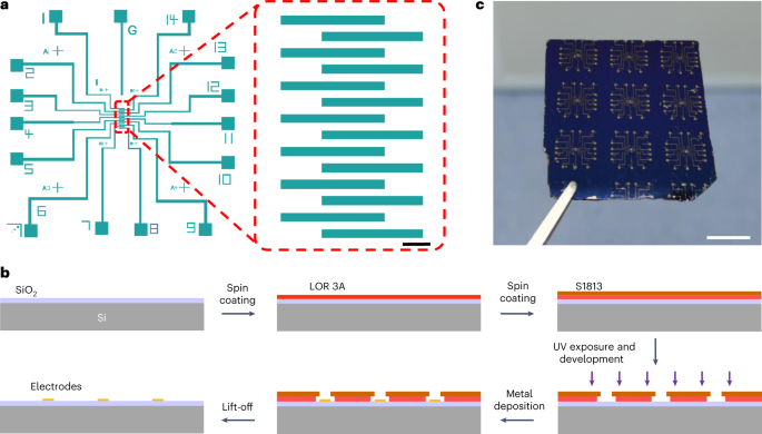
a, Electrode pattern drawn by CleWin for a direct-write optical lithography system. Scale bar, 100 µm. b, Procedure for fabricating the electrodes. A bilayer lift-off strategy (LOR3A/S1813) is used in the photolithography process. c, Photograph of the electrodes patterned on SiO2/Si. Scale bar, 1 cm.
-
23
Wash a 4-inch silicon wafer sequentially in acetone, ethanol and deionized (DI) water. Dry the substrate with a compressed nitrogen gun.
-
24
Bake the wafer at 180 °C for 5 min to remove residual moisture and solvent. Then, cool the wafer down to RT for 1 min.
Critical step
The resist is sensitive to the humidity level in the clean room during spinning. Ensure that the ambient humidity level is <50% or make sure that the wafer is dehydrated before spinning the resist.
-
25
Place the wafer in the spinner chuck and ensure that it is centered. Open the vacuum to seal the wafer tightly on the chuck. Dispense 5 ml of LOR 3A resist at the wafer center and run the spin-coating program as follows: (i) spin the wafer at 500 rpm with acceleration of 100 rpm/s for 10 s, and (ii) ramp the speed up to 4,000 rpm with acceleration of 500 rpm/s and hold it for 60 s before ramping down.
-
26
Bake the LOR 3A resist on the hot plate at 170 °C for 1 min. Then, let the wafer cool down to RT for 1 min.
-
27
Place the wafer back on the chuck and open the vacuum. Dispense 5 ml of S1813 photoresist and run the same program as in Step 25.
-
28
Bake the S1813 photoresist on the hot plate at 115 °C for 1 min. Then, cool the wafer down at RT for 1 min.
Critical step
The bilayer lift-off process (Fig. 9b) of spinning LOR 3A and S1813 is important to improve the lift-off efficiency because of the resulting undercut after development.
-
29
Put the wafer on the chuck center of a direct-write optical lithography system and load the electrode pattern into the software. Then, expose the electrode pattern on the wafer at an intensity of 135 mJ/cm2.
-
30
Immerse the wafer in an MF-321 developer for 1 min and rinse it with DI water. Dry the wafer with the compressed nitrogen gun.
-
31
Check the electrode patterns on the wafer under an optical microscope.
Critical step
If any resist residue is left on the exposed patterns, put the wafer in the oxygen plasma etcher at 50 W for 1 min.
-
32
Load the wafer face down onto the sample holder of a thermal evaporator system. Activate the pump and wait until the chamber vacuum is <6 × 10⁻⁶ Torr. Set parameters for chromium and gold. The thickness of chromium is 5 nm, and the deposition rate is 1 Å/s. The thickness of gold is 40 nm, with a deposition rate of 2 Å/s.
Critical step
Do not open the chamber after chromium deposition, because exposure of the chromium layer to oxygen severely damages the adhesive strength between the chromium and gold layers.
-
33
Unload the wafer after ventilation of the thermal evaporator system. Bake the wafer on the hot plate at 180 °C for 1 min to allow photoresist reflow and cool the wafer at RT for 1 min.
-
34
Immerse the wafer in Remover PG and bake it on a hot plate at 60 °C for 30 min for lift-off.
-
35
Rinse the wafer sequentially with ethanol and DI wafer. Then, dry the wafer by using a compressed nitrogen gun (Fig. 9c).
-
36
Observe the electrode under an optical microscope to check if the resist is completely stripped. If resist residue is left on the wafer, put the wafer in the oxygen plasma etcher at 50 W for 1 min.

Graphene synthesis, transfer and patterning
Timing ~7 h
Caution
Keep the vacuum pump at the end of the tube furnace turned on throughout the process to avoid possible leakage of flammable gas. No open flame is allowed in the laboratory.
Critical
Introduce both H2 and CH4 to the tube furnace at constant flow for 15 min before turning on the power to expel any air remaining in the gas tube.
-
37
Cut copper foil into several 2 × 5 cm2 pieces and put them in the center of the tube furnace. Activate the pump and wait until the vacuum is <10−3 Torr.
-
38
Open the H2 valve and introduce the gas at a flow rate of 4 standard cubic centimeters per minute (sccm).
Critical step
Maintain H2 flow throughout the graphene growth process to provide a reductive environment.
-
39
Ramp the temperature to 1,000 °C in 30 min and hold it for another 30 min.
-
40
Open the CH4 valve and introduce the gas at a flow rate of 16 sccm for 15 min during the graphene growth process (Fig. 10a).
Fig. 10: Graphene synthesis, transfer and patterning. 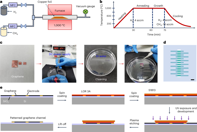
a, Schematic of the chemical vapor deposition system. Source gases are introduced to the furnace through a mass flow controller (MFC) for graphene growth on copper foil. b, Time line of the furnace temperature for graphene growth. H2 at a flow rate of 4 sccm is introduced throughout the growth process to provide a reductive environment, and CH4 at 16 sccm is introduced for graphene growth. c, Procedure for the graphene transfer onto the device. Graphene is exfoliated from the copper foil via an electrochemical bubbling transfer method at a voltage of 2.4 V. After cleaning with DI water, the graphene film is picked up by the fabricated device. d, The CleWin file for graphene patterning, in which the area in light blue is exposed. Scale bar, 100 µm. e, Photolithography procedure for patterning graphene.
-
41
Turn off the power and cool the tube furnace to RT. Then, take the copper foil out of the furnace (Fig. 10b).
-
42
Tape the copper foil on a glass slide with Kapton polyimide tape. Then, put the glass slide in the center of the spinner chuck.
-
43
Dispense 3 ml of PMMA on the copper foil and run the spin-coating program: (i) spin the slide at 500 rpm with acceleration of 100 rpm/s for 10 s, and (ii) ramp the speed up to 3,000 rpm with acceleration of 500 rpm/s and hold it for 60 s before ramping down.
-
44
Bake the glass slide on a hot plate at 180 °C for 1 min.
-
45
Peel off the copper foil from the glass slide and put the foil upside down. Then, etch the graphene that has grown on the back side of the copper foil with oxygen plasma at 50 W for 30 s.
-
46
Cut the copper foil into 3 × 3 mm2 pieces and connect the copper foil to the negative voltage terminal of the power supply. Then, exfoliate the graphene/PMMA in a 0.5 mM NaOH solution at a bias voltage of 2.4 V via the electrochemical bubbling method (Fig. 10c).
-
47
Transfer the PMMA-carried graphene film to a culture dish filled with ultrapure water. Incubate the dish for 1 h at RT.
-
48
Use a fabricated electrode substrate to pick up the floating graphene/PMMA film to connect the source and drain electrodes.
Critical step
If the surface of the electrode device is hydrophobic, treat the electrode device with oxygen plasma to avoid wrinkles that may occur.
-
49
Dry the device naturally in the ambient condition at RT. Then, bake the device on a hot plate at 180 °C for 1 h.
-
50
Immerse the device in acetone on a hot plate at 50 °C for 30 min to remove PMMA.
Critical step
Use PMMA with a lower molecular weight or thermally anneal the graphene-transferred device in the tube furnace while introducing argon gas if PMMA residue remains on the graphene.
-
51
Rinse the device sequentially with ethanol and DI water. Dry it with a compressed nitrogen gun.
-
52
Repeat Steps 22‒31 to pattern the graphene channel by using the graphene patterning CleWin file (Fig. 10d). Protect the defined graphene sensing channel with resist (Fig. 10e).
Critical step
Use LOR 3A/S1813 bilayer resist for the photolithography to pattern the graphene, because the S1813 residue easily remains on the graphene and is hard to remove with acetone.
-
53
Etch the graphene film except the channel region with oxygen plasma at 50 W for 1 min.
-
54
Immerse the device in MF-321 developer for 30 min to remove the resist. Then, rinse thoroughly with DI water and dry with a compressed nitrogen gun.
Critical step
Use MF-321 developer rather than Remover PG to remove the resist after graphene patterning, because Remover PG may damage the graphene.

MolEMS functionalization on graphene
Timing ~6 h
-
55
Immerse the fabricated transistor device in 5 mM PASE solution for 2 h at RT. After that, rinse the device thoroughly with ethanol and DI water and dry the device with a compressed nitrogen gun.
-
56
Cut the cured PDMS (see Reagent setup) into a 1 × 1 cm2 piece and prepare a PDMS well by punching the center with a 3-mm-diameter punch.
-
57
Place the PDMS well above the graphene sensing region of the fabricated transistor device from Step 55. Then, add 100 µl of MolEMS solution in the PDMS well and incubate for ≥4 h at RT.
Critical step
Gently press the PDMS well downward before adding solution to avoid possible leakage.
-
58
Replace the MolEMS solution with 1× TM buffer for storage.
Pause point
Store at 4 °C in the dark for long-term storage. Cover the PDMS well with a glass slide to prevent evaporation of the solution.
-
59
Characterize the functionalization of MolEMS on graphene via AFM, X-ray photoelectron spectrometry or Raman spectroscopy. If possible, AFM is preferable because it allows direct observation of MolEMS structures on graphene45. X-ray photoelectron spectrometry or Raman spectroscopy serve as supplementary characterization54.
Critical step
The AFM image of MolEMS-modified graphene should be obtained in 1× TM buffer to improve the resolution.
Electrostatic actuation of MolEMS
Timing ~0.5 h
-
60
Repeat Steps 22‒36 to fabricate electrodes on a quartz slide.
-
61
Repeat Steps 46‒51 to transfer graphene onto the electrode.
-
62
Repeat Steps 1‒6 to synthesize MolEMS with the end of the cantilever modified with Cy3 fluorescent dye (Table 4).
Table 4 ssDNAs for assembling the MolEMS used in electrostatic actuation characterization -
63
Repeat Steps 55‒59 to functionalize MolEMS on the graphene.
-
64
Put the quartz slide on the stage of a confocal fluorescence microscope and insert an Ag/AgCl electrode into the PDMS well (Fig. 11a).
Fig. 11: Characterization of electrostatic actuation. 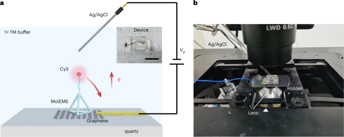
a, Schematic of the fluorescence-quenching experiment. The MolEMS modified with Cy3 at the end of the ssDNA is immobilized on graphene. The electrostatic actuation moves the Cy3 to the graphene surface, inducing fluorescence quenching. Inset: the fabricated device (scale bar, 1 cm). b, Experimental setup. The device is mounted on the holder, and an Ag/AgCl electrode is inserted into the PDMS well. The fluorescence at different Vg values is imaged.
-
65
Connect the electrode on the glass slide and the inserted Ag/AgCl electrode to a mobile power supply.
Critical step
The Ag/AgCl electrode should be connected to the negative voltage terminal of the power supply so that the DNA cantilever of MolEMS can be actuated toward the graphene surface.
-
66
Image the fluorescence intensity by tusing he confocal fluorescence microscope at Vg = 0.9 V, Vg = 0 V and Vg = ‒1.1 V under 561-nm excitation wavelength (Fig. 11b).

Electrical measurements
Timing variable
Measurement setup
-
67
Mount the MolEMS FET device on a custom-designed PCB and wire bond the source and drain contact pads to pads on the board (Fig. 12 and Supplementary Fig 4).
Fig. 12: Electrical measurement setup. 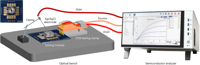
The MolEMS g-FET is wire bonded to a designed PCB (scale bar, 1 cm) that is clamped by a 4-pin PCB testing clamp and put on an optical bench. The inserted Ag/AgCl electrode along with the source and drain electrode are connected to a semiconductor analyzer.
Critical step
Wire bonding is important to reduce the noise level. Observe the patterned graphene channels under an optical microscope and choose one graphene channel with no obvious defects for the wire bonding and electrical measurements afterwards.
-
68
Connect the source and drain electrodes to a semiconductor analyzer through a 4-pin PCB testing clamp.
-
69
Insert an Ag/AgCl reference electrode in the liquid and connect it to the semiconductor analyzer.

Transport curve measurements
-
70
Prepare thrombin solution in TRB buffer by serial dilution from stock thrombin solution (see Reagent setup), with concentrations of 5 × 10⁻¹⁹ M, 5 × 10⁻¹⁸ M, 5 × 10⁻¹⁶ M, 2.5 × 10⁻¹³ M, 2.5 × 10⁻¹² M, 2.5 × 10⁻¹¹ M, 2.5 × 10⁻¹⁰ M and 5 × 10⁻¹⁰ M.
Critical step
Warm the stock solution to RT before dilution. Avoid repeated freezing and thawing.
-
71
Gently fill the PDMS well with TRB buffer. Set Vds at 50 mV and sweep the Vg from ‒0.4 to 0.6 V, with a step of 5 mV.
-
72
Run the sweeping program and simultaneously record the Ids. Measure the transport curve several times before adding analytes until the transport curve does not drift.
-
73
Replace the PDMS well with BSA and casein solution at 5 × 10⁻¹⁵ M (in TRB buffer) and incubate for 15 min. Then, measure the transport curve again with the parameters as listed in Step 71.
-
74
Repeat Step 73 by replacing the solution in the PDMS well with thrombin solutions with increased concentration. Perform three repeated measurements.
Time-resolved current measurements
-
75
Add TRB buffer to the PDMS well. Set Vds at 50 mV and Vg at 0 V.
-
76
Run the program by recoding the real-time Ids in TRB buffer until the value stabilizes.
-
77
Replace the PDMS well with BSA and casein solution at 5 × 10⁻¹⁵ M (in TRB buffer) and incubate the sample until the Ids response reaches an equilibrium state.
-
78
Repeat Step 77 to replace the PDMS well with thrombin solutions of increased concentration. Perform three repeated measurements.
Electromechanical testing
-
79
Add TRB buffer to the PDMS well. Then, set Vds at 50 mV and an appropriate negative Vg.
-
80
Repeat Steps 77‒78 to measure the real-time Ids response upon addition of thrombin solutions with increased concentration.
Characterizing the antifouling properties of MolEMS
-
81
Repeat Step 71 to measure the transport curve of the MolEMS FET in PBS buffer.
-
82
Replace the PBS with full serum and incubate for 30 min.
-
83
Rinse the graphene surface with PBS buffer by gently pipetting.
-
84
Replace the serum in the PDMS well with fresh PBS buffer. Then, run the program to measure the transport curve again.
Application of the MolEMS for measuring Hg2+ levels in solution
Timing ~2 h
Critical
When testing analytes, perform three repeated measurements of them.
-
85
Repeat Steps 1‒6 and 55‒58 to synthesize and functionalize the MolEMS for Hg2+ detection (Table 4).
-
86
Prepare Hg2+ solutions in 1× TM buffer at the same concentration range as in Step 70. Dissolve Hg(NO3)2 in HNO3 first, followed by serial dilution in 1× TM buffer.
-
87
Add solutions of control ions such as Fe3+, Cd2+, Zn2+, Ca2+ and Cu2+ (in 1× TM buffer) at 5 × 10⁻¹⁵ M before Hg2+ to verify the specificity. One or multiple control ion solutions can be used to verify the specificity of the measurement, where the ion solution is prepared by dissolving corresponding metallic salt in the 1× TM buffer.
-
88
Measure the real-time Ids response upon consecutive addition of Hg2+ solutions with increased concentration as in Steps 77‒78 at an appropriate negative Vg.
Application of the MolEMS for measuring ATP levels in solution
Timing ~2 h
-
89
Repeat Steps 1‒6 and 55‒58 to synthesize and functionalize the MolEMS for ATP detection (Table 4).
-
90
Prepare ATP solutions in 1× AM buffer at the same concentration range as in Step 70.
-
91
Add CTP and GTP solutions at 5 × 10⁻¹⁵ M (in 1× AM buffer) sequentially before ATP to verify the specificity.
-
92
Measure the real-time Ids response upon consecutive addition of ATP solutions with increased concentration as in Steps 77‒78 at an appropriate negative Vg.
Application of MolEMS for measuring ss-DNA-T levels in solution
Timing ~2 h
-
93
Repeat Steps 1‒6 and 55‒58 to synthesize and functionalize the MolEMS for ssDNA-T detection (Table 5).
Table 5 ssDNAs for assembling the MolEMS to measure Hg2+, ATP and ssDNA-T -
94
Prepare ssDNA-T solutions in serum at the same concentration range as in Step 70.
-
95
Add solutions of ssDNA (in serum) with random sequences (ssDNA-R1 to R3) and each of the three ssDNA sequences with one-base mismatches at different locations (ssDNA-mis-3′, ssDNA-mis-m and ssDNA-mis-5′; Supplementary Table 1) to verify the specificity of the measurement.
-
96
Measure the real-time Ids response upon consecutive addition of ssDNA-T solutions with increased concentration as in Steps 77‒78 at an appropriate negative Vg.
Application of the MolEMS for measuring SARS-CoV-2 cDNA levels in solution
Timing ~2 h
Critical
Cell culture, RNA extraction and reverse transcription should be performed in a BSL-3 environment. Researchers must wear suitable PPE and respirators. All work with infectious agents or toxins must be performed within an appropriate biosafety cabinet.
-
97
Culture African green monkey kidney cell line Vero E6 at 37 °C with 5% CO2 in DMEM.
-
98
Propagate SARS-CoV-2 strain nCoV-SH01 (GenBank, MT121215.1) from a laboratory-confirmed COVID-19 severe pneumonia case provided from CDC Shanghai in Vero E6 cells in a BSL-3 laboratory.
-
99
Extract viral RNA from Vero E6 cells (102–106 cells) by using TRIzol reagent and following the manufacturer’s instructions.
-
100
Reverse-transcribe the viral RNA to cDNA by using the SuperScript III CellsDirect cDNA synthesis kit and following the manufacturer’s instructions.
-
101
Quantify the viral cDNA via qRT–PCR by using the Tiangen qRT–PCR detection kit and following the manufacturer’s instructions.
-
102
Serially dilute the viral cDNA in artificial saliva to cDNA concentrations of 500, 50, 5, 0.5, 0.1 and 0.02 copies/μl.
-
103
Repeat Steps 1‒6 and 55‒58 to synthesize and functionalize the MolEMS for SARS-CoV-2 cDNA detection (Table 5).
-
104
Add SARS-CoV, MERS-CoV IVT RNA and human cDNA dissolved at 0.5 copies/μl (in artificial saliva) sequentially before SARS-CoV-2 cDNA to verify the specificity.
-
105
Measure the real-time Ids response upon addition of SARS-CoV-2 cDNA at different concentrations.
Application of the MolEMS for measuring SARS-CoV-2 IVT RNA levels in solution
Timing ~2 h
-
106
Repeat Step 102 to prepare serial dilutions of SARS-CoV-2 IVT RNA. Add RNase inhibitor (2%) in the testing buffer for RNA dilution to avoid RNA degradation.
-
107
Repeat Steps 1‒6 and 55‒58 to synthesize and functionalize the MolEMS for SARS-CoV-2 IVT RNA detection (Table 5).
-
108
Add SARS-CoV, MERS-CoV IVT RNA and human cDNA dissolved at 0.5 copies/μl (in artificial saliva) sequentially before SARS-CoV-2 IVT RNA to verify the specificity of the measurement.
-
109
Measure the Ids response upon addition of SARS-CoV-2 IVT RNA at different concentrations.
Testing clinical SARS-CoV-2 samples by the MolEMS
Timing ~0.5 h
Caution
Experiments involving human participants must have ethical approval by the appropriate health authority and after obtaining patient consent. The experiments presented in our primary research paper45 were approved by the Shanghai Public Health Clinical Center Ethics Committee.
Critical
Healthcare providers collecting specimens or working within 6 feet of patients suspected of being infected with SARS-CoV-2 must wear appropriate PPE, which includes an N95 or higher-level respirator (or face mask if a respirator is not available), eye protection, gloves and a gown.
-
110
Repeat Steps 1‒6 and 55‒58 to synthesize and functionalize the MolEMS for SARS-CoV-2 RNA detection (Table 6).
Table 6 ssDNAs for assembling the MolEMS used in SARS-CoV-2 nucleic acid testing -
111
Insert a swab into the posterior pharynx and tonsillar areas of the patient. Rub the swab over both tonsillar pillars and the posterior oropharynx.
-
112
Put the swab sample in VTM and heat the sample at 56 °C for 30 min to inactivate the virus and release viral RNA. Then, cool the sample down to RT.
-
113
Add samples from patients with fever or influenza and from healthy participants before the clinical SARS-CoV-2 sample to verify the specificity of the measurements. The control samples are treated as in Step 112.
-
114
Add the SARS-CoV-2 sample in the PDMS well and measure the Ids response (Fig. 13).
Fig. 13: Workflow of SARS-CoV-2 nucleic acid testing by the MolEMS g-FET. 
i, SARS-CoV-2 virus samples are obtained from patients and put in VTM. ii, Virus inactivation and viral RNA release at 56 °C for 30 min. iii, Sample testing by the MolEMS g-FET. Figure adapted from ref. 54, American Chemical Society.

Analysis of the electrical signal
Timing variable
Real-time current measurements
-
115
Save the output of the measured Ids response as an individual csv file. The baseline Ids before addition of the analyte is Ids,0. Ids changes when the probe is exposed to analyte. The change in Ids with respect to Ids,0 is ΔIds.
-
116
Use Origin software to extract the ΔIds upon addition of analyte-containing solution at different concentrations, where the Ids at that concentration reaches an equilibrium state. Then, normalize the response by dividing ΔIds by Ids,0 (Fig. 14a).
Fig. 14: Analysis of real-time current measurement. 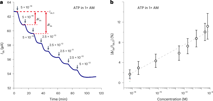
a, Ids versus time curve upon addition of ATP at different concentrations. b, |ΔIds/Ids,0| response upon different analyte concentrations is extracted as highlighted in a. The signal is normalized to |ΔIds/Ids,0| and plotted as a function of analyte concentration. Error bars show the standard deviation of three measurements. Figure adapted from ref. 45, Springer Nature Ltd.
-
117
Calculate the average ΔIds/Ids,0 response for each analyte concentration by using the three repeated measurements obtained at Steps 88, 92, 96, 105 and 109 (Fig. 14b).

Noise analysis and LoD estimation
-
118
Analyze the noise level of the Ids signal in each blank testing solution (Fig. 15a). Set a cutoff noise level for the valid response to each analyte as three times the noise level.
Fig. 15: Noise analysis and LoD estimation. 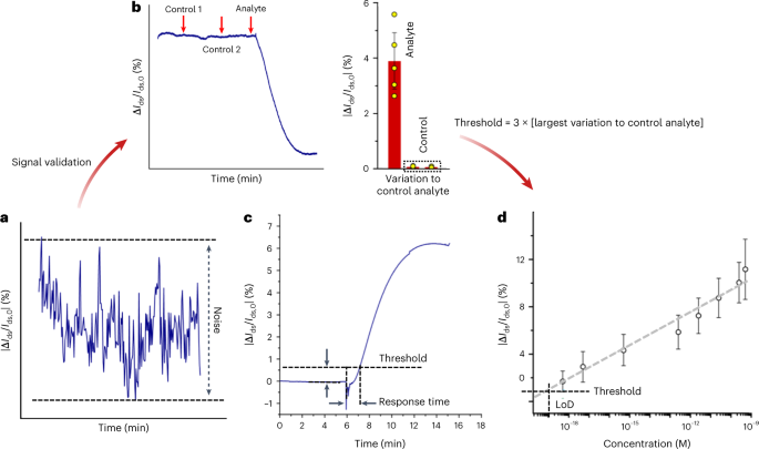
a, Noise of the ΔIds/Ids,0 response in blank testing buffer. b, The relative current variation is calculated in a negative control assay. The response variation to the control analyte is taken as the level of noise. c and d, Estimation of response time and LoD for analyte testing by extracting the intercept of the threshold response level with real-time ΔIds/Ids,0 responses and fitting a curve of binding kinetics. The threshold response level is calculated as noise in a blank testing solution plus three times the of level of noise obtained from the largest response variation to control analytes. Error bars show the standard deviation of three measurements. Panels b and d adapted from ref. 45, Springer Nature Ltd.
-
119
Compare the measured ΔIds response upon addition of analyte with the cutoff noise level to evaluate the validity of the measured response.
-
120
Calculate the largest relative current variation in the negative control assay in the same testing solution and take three times the largest variation as the threshold value (Fig. 15b).
-
121
Extract the response time as the intercept of the threshold response level and the real-time ΔIds/Ids,0 responses (Fig. 15c).
-
122
Plot the average ΔIds/Ids,0 response as a function of analyte concentration.
-
123
Fit the experimental data to the following binding kinetics model through Origin software
$$\left| {\Delta I_{{{{\mathrm{ds}}}}}\,/\,I_{{{{\mathrm{ds}}}},0}} \right| = A_\mathrm{{max}}\frac{{\left( {\left[ C \right]\,/\,K_{{{\mathrm{d}}}}} \right)^n}}{{1 + \left( {\left[ C \right]\,/\,K_{{{\mathrm{d}}}}} \right)^n}}$$where Amax is the saturation |ΔIds/Ids,0| response, [C] is the analyte concentration, Kd is the equilibrium dissociation constant and n is the Hill coefficient corresponding to the binding cooperativity.
-
124
Extract the analyte concentration at the intercept of the threshold response level and the fitting curve obtained in Step 123 to obtain the LoD (Fig. 15d).

Constructing a portable testing system
Timing variable
-
125
Draw the circuits in Altium Designer 20 software including signal-acquisition circuits and data-processing and readout circuits (Fig. 16a and Supplementary Fig. 6). Lay all the circuits on a two-layer PCB board (Fig. 16b).
Fig. 16: Portable testing system. 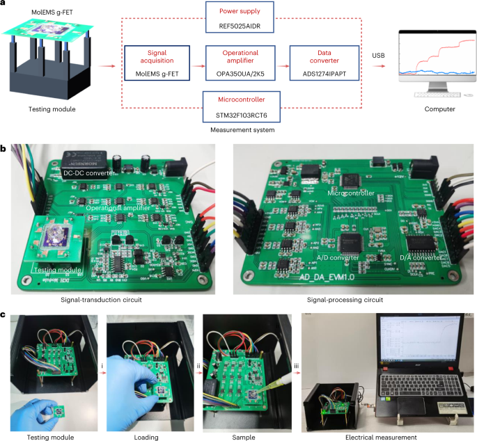
a, Design of the portable testing system. b, PCBs for signal processing and transduction, including microcontroller, testing module, DC-DC converter, operational amplifier, analog-to-digital (A/D) converter, D/A converter and testing module. c, The procedure for using the portable system for analyte testing, including testing module loading, sample loading and electrical measurement.
-
126
Outsource the two-layer PCB for manufacture to eluton PCB or another suitable manufacturer using standard seven-step procedures: patterning, photoengraving, lamination, drilling, solder plating, silk screen and testing.
-
127
Attach all electronic components onto the resulting PCB by automatic welding.
-
128
Connect each PCB with a DuPont line of a designed arranged sequence from the signal processing board to the signal-transduction board.
-
129
Turn on a customized power supply. The PCB is powered by either a 220 V AC or rechargeable nickel-metal hydride batteries (4.8 V, 2,800 mAh) through the customized circuit module.
-
130
Connect standard resistors such as 1 kΩ, 10 kΩ and 1 MΩ to calibrate the signal-acquisition circuits and data-processing circuits.
-
131
Use the fabricated PCB to measure the transistor’s electrical properties to validate the stability and reliability of the PCB.
-
132
Repeat Step 67 to prepare the testing module.
-
133
Load the testing module onto the portable system and connect the system to a computer by USB (Fig. 16c).
-
134
Run the current measurement program and then add the testing sample.
-
135
Measure the real-time current response and read the results from the computer.

Troubleshooting
Troubleshooting advice can be found in Table 7.
Timing
-
Steps 1–6, MolEMS synthesis: ~1 h
-
Steps 7–21, MolEMS characterization: ~5.5 h
-
Steps 22–36, electrode fabrication: ~4 h
-
Steps 37–54, graphene synthesis, transfer and patterning: ~7 h
-
Steps 55–59, MolEMS functionalization on graphene: ~6 h
-
Steps 60–66, electrostatic actuation of MolEMS: ~0.5 h
-
Steps 67–84, electrical measurements: variable
-
Steps 85–88, application of MolEMS for measuring Hg2+ levels in solution: ~2 h
-
Steps 89–92, application of MolEMS for measuring ATP levels in solution: ~2 h
-
Steps 93–96, application of MolEMS for measuring ssDNA-T levels in solution: ~2 h
-
Steps 97–105, application of MolEMS for measuring SARS-CoV-2 cDNA levels in solution: ~2 h
-
Steps 106–109, application of MolEMS for measuring SARS-CoV-2 IVT RNA levels in solution: ~2 h
-
Steps 110–113, testing clinical SARS-CoV-2 samples by MolEMS: ~0.5 h
-
Step 114, the response time from adding sample to result read-out: 4 min
-
Steps 115–124, analysis of electrical signal: variable
-
Steps 125–135, constructing a portable testing system: variable
Anticipated results
Integration of a MolEMS and a FET enables ultrasensitive electromechanical detection of trace analytes in biofluids. If you assemble a MolEMS by following the procedures presented in this protocol, you can expect results similar to those shown in Fig. 4. If you perform the fabrication of the g-FET device, you can expect results similar to those in Fig. 2c. If you functionalize a graphene surface with a MolEMS, you can expect results similar to those shown in Fig. 2d. The electrostatic actuation of MolEMS at the interface of a graphene FET enables ultrasensitive electromechanical sensing of analytes, including thrombin, Hg2+, ATP and nucleic acids, with an LoD of seveal copies for nucleic acid and ~10−19 M for thrombin, Hg2+ and ATP in 100 μl of testing solution. The MolEMS g-FET shows an overall ΔIds/Ids,0 exceeding 1.2% to all types of analyte at 5 × 10⁻¹⁶ M in both buffer and full serum (Fig. 17a). Moreover, the electromechanical detection strategy based on the MolEMS is universal and could be applied to other biomarkers by following the procedures for MolEMS design and assemblage, provided that commercial bioreceptor molecules exist or that aptamers can be synthesized via the systematic evolution of ligands by exponential enrichment process.

a, |ΔIds/Ids,0| responses of MolEMS g-FETs on the addition of target analytes (5 × 10⁻¹⁶ M) of thrombin, ATP, Hg2+, ssDNA-T and non-target (5 × 10⁻¹⁵ M) analytes (casein, BSA, CTP, GTP, Fe3+, Cd2+, Zn2+, Ca2+ and Cu2+). Error bars show the standard deviation of three measurements. b, Real-time ΔIds/Ids,0 response upon addition of fever patient sample F1, COVID-19 patient sample P1 (6%) and P1 (100%). The inset is the box plot of the response time for clinical samples P1–P26. c, |ΔIds/Ids,0| responses to each clinical sample. ‘×10’ indicates 10 times the |ΔIds/Ids,0| (for F1–F23, A1–A4, B1, B2 and H1–H25). Figure reproduced from ref. 45, Springer Nature Ltd; the experiment reported therein was approved by the Shanghai Public Health Clinical Center Ethics Committee.
The practical application of the MolEMS technique in the real world is demonstrated by SARS-CoV-2 nucleic acid detection in patient samples, including PCR-confirmed positive COVID-19 samples P1‒P33, negative control fever samples F1‒F23, influenza A samples A1‒A4, influenza B samples B1‒B2 and samples of healthy volunteers H1‒H25. The MolEMS g-FET shows an appreciable response to positive COVID-19 samples and a negligible response to control samples (Fig. 17c). By following Steps 120 and 121, the response time is estimated to be <4 min (Fig. 17b). Meanwhile, the assay sensitivity is maintained in serially diluted clinical samples (Extended Data Fig. 5). Integration of the MolEMS gFET with the portable testing system described in this protocol should allow on-site pathogen screening, disease diagnosis and environmental monitoring to be achieved.
The core MolEMS g-FET device is the disposable sensing unit, which is inserted and connected to the main measurement system. When a sample is introduced to the testing module, the anticipated real-time current response resembles that in Fig. 17b. It should be noted that, because the liquid-gated FET is sensitive to surface charge perturbations, when adding real samples with different ionic conditions than those of the reference solution in the PDMS well, you should expect a stepwise Ids response of the FET before the binding of analyte occurs. In this case, you should use the same testing solution as the sample in the PDMS well as the reference or subtract the stepwise signal from the total Ids response if the reference solution is not available.
Calibration of the MolEMS g-FET output performance is essential for analyte quantification. For the affinity-based binding, the correlation between response and analyte concentration follows the Hill-Langmuir model, which can be used for analyte quantification. The greatest barrier to accurate analyte quantification is response reproducibility, which is hindered by device-to-device deviation. This deviation mainly comes from the nonuniformity of the transistor’s output performance and the surface functionalization. Although great efforts have been directed to the standardization of device preparation and signal normalization, the deviation has been challenging to eliminate. To further improve testing accuracy, multiple identical sensing channels can be integrated on a single chip for statistical analysis of the measured signal. Alternatively, a differential testing scheme can be designed whereby a bare g-FET channel serves as a compensation unit for the sensing unit to mitigate the effects of non-specific interference or the ambient environment.
Data availability
The data supporting the findings of this study are available within the article, its Supplementary Information and the supporting primary research paper45. Source data are provided with this paper.
Code availability
The CleWin files used in this protocol are provided in the Supplementary Information.
References
Anichini, C. et al. Chemical sensing with 2D materials. Chem. Soc. Rev. 47, 4860–4908 (2018).
Banerjee, I., Pangule, R. C. & Kane, R. S. Antifouling coatings: recent developments in the design of surfaces that prevent fouling by proteins, bacteria, and marine organisms. Adv. Mater. 23, 690–718 (2011).
Gooding, J. J. & Gaus, K. Single‐molecule sensors: challenges and opportunities for quantitative analysis. Angew. Chem. Int. Ed. Engl. 55, 11354–11366 (2016).
Sabaté del Río, J., Henry, O. Y., Jolly, P. & Ingber, D. E. An antifouling coating that enables affinity-based electrochemical biosensing in complex biological fluids. Nat. Nanotechnol. 14, 1143–1149 (2019).
Wu, J. et al. Two-dimensional molybdenum disulfide (MoS2) with gold nanoparticles for biosensing of explosives by optical spectroscopy. Sens. Actuators B Chem. 261, 279–287 (2018).
Wang, Y. et al. Biosensor based on hydrogel optical waveguide spectroscopy. Biosens. Bioelectron. 25, 1663–1668 (2010).
Schröder, L., Lowery, T. J., Hilty, C., Wemmer, D. E. & Pines, A. Molecular imaging using a targeted magnetic resonance hyperpolarized biosensor. Science 314, 446–449 (2006).
Ozbakir, H. F. et al. A protein-based biosensor for detecting calcium by magnetic resonance imaging. ACS Sens. 6, 3163–3169 (2021).
Marko-Varga, G., Johansson, K. & Gorton, L. Enzyme-based biosensor as a selective detection unit in column liquid chromatography. J. Chromatogr. A 660, 153–167 (1994).
Kim, S.-W., Cho, I.-H., Lim, G.-S., Park, G.-N. & Paek, S.-H. Biochemical-immunological hybrid biosensor based on two-dimensional chromatography for on-site sepsis diagnosis. Biosens. Bioelectron. 98, 7–14 (2017).
Jafari, M., Khayamian, T., Shaer, V. & Zarei, N. Determination of veterinary drug residues in chicken meat using corona discharge ion mobility spectrometry. Anal. Chim. Acta 581, 147–153 (2007).
Kalhor, H. & Alizadeh, N. Determining urea levels in dialysis human serum by means of headspace solid phase microextraction coupled with ion mobility spectrometry and on the basis of nanostructured polypyrrole film. Anal. Bioanal. Chem. 405, 5333–5339 (2013).
Zangar, R. C., Daly, D. S. & White, A. M. ELISA microarray technology as a high-throughput system for cancer biomarker validation. Expert Rev. Proteom. 3, 37–44 (2006).
De La Rica, R. & Stevens, M. M. Plasmonic ELISA for the ultrasensitive detection of disease biomarkers with the naked eye. Nat. Nanotechnol. 7, 821–824 (2012).
Jacobs, M., Muthukumar, S., Selvam, A. P., Craven, J. E. & Prasad, S. Ultra-sensitive electrical immunoassay biosensors using nanotextured zinc oxide thin films on printed circuit board platforms. Biosens. Bioelectron. 55, 7–13 (2014).
Gao, Y. et al. Multiplex measurement of twelve tumor markers using a GMR multi-biomarker immunoassay biosensor. Biosens. Bioelectron. 123, 204–210 (2019).
Gibani, M. M. et al. Assessing a novel, lab-free, point-of-care test for SARS-CoV-2 (CovidNudge): a diagnostic accuracy study. Lancet Microbe 1, e300–e307 (2020).
Nalla, A. K. et al. Comparative performance of SARS-CoV-2 detection assays using seven different primer-probe sets and one assay kit. J. Clin. Microbiol. 58, e00557–e00520 (2020).
Chinnadayyala, S. R. et al. Recent advances in microfluidic paper-based electrochemiluminescence analytical devices for point-of-care testing applications. Biosens. Bioelectron. 126, 68–81 (2019).
Jameison, F. et al. Electrochemiluminescence-based quantitation of classical clinical chemistry analytes. Anal. Chem. 68, 1298–1302 (1996).
Yang, S., Dai, X., Stogin, B. B. & Wong, T.-S. Ultrasensitive surface-enhanced Raman scattering detection in common fluids. Proc. Natl Acad. Sci. USA 113, 268–273 (2016).
McNay, G., Eustace, D., Smith, W. E., Faulds, K. & Graham, D. Surface-enhanced Raman scattering (SERS) and surface-enhanced resonance Raman scattering (SERRS): a review of applications. Appl. Spectrosc. 65, 825–837 (2011).
Haes, A. J., Hall, W. P., Chang, L., Klein, W. L. & Van Duyne, R. P. A localized surface plasmon resonance biosensor: first steps toward an assay for Alzheimer’s disease. Nano Lett. 4, 1029–1034 (2004).
Homola, J., Lu, H. B., Nenninger, G. G., Dostálek, J. & Yee, S. S. A novel multichannel surface plasmon resonance biosensor. Sens. Actuators B Chem. 76, 403–410 (2001).
Karyakin, A. A., Puganova, E. A., Bolshakov, I. A. & Karyakina, E. E. Electrochemical sensor with record performance characteristics. Angew. Chem. Int. Ed. Engl. 46, 7678–7680 (2007).
Lu, Y., Yang, Q. & Wu, J. Recent advances in biosensor-integrated enrichment methods for preconcentrating and detecting the low-abundant analytes in agriculture and food samples. Trends Anal. Chem. 128, 115914 (2020).
Jiang, Y. et al. Aptamer/AuNP biosensor for colorimetric profiling of exosomal proteins. Angew. Chem. Int. Ed. Engl. 56, 11916–11920 (2017).
Jiang, C. et al. Antifouling strategies for selective in vitro and in vivo sensing. Chem. Rev. 120, 3852–3889 (2020).
Kimball, S. R. & Jefferson, L. S. Signaling pathways and molecular mechanisms through which branched-chain amino acids mediate translational control of protein synthesis. J. Nutr. 136, 227S–231S (2006).
Wilkinson, K. D. et al. Metabolism of the polyubiquitin degradation signal: structure, mechanism, and role of isopeptidase T. Biochemistry 34, 14535–14546 (1995).
Yang, Z. & Klionsky, D. J. Mammalian autophagy: core molecular machinery and signaling regulation. Curr. Opin. Cell Biol. 22, 124–131 (2010).
Nathanson, H. C., Newell, W. E., Wickstrom, R. A. & Davis, J. R. The resonant gate transistor. IEEE Trans. Electron Devices 14, 117–133 (1967).
Ohno, Y., Maehashi, K. & Matsumoto, K. Label-free biosensors based on aptamer-modified graphene field-effect transistors. J. Am. Chem. Soc. 132, 18012–18013 (2010).
Zhang, A. & Lieber, C. M. Nano-bioelectronics. Chem. Rev. 116, 215–257 (2016).
Nakatsuka, N. et al. Aptamer–field-effect transistors overcome Debye length limitations for small-molecule sensing. Science 362, 319–324 (2018).
Hwang, M. T. et al. DNA nanotweezers and graphene transistor enable label‐free genotyping. Adv. Mater. 30, 1802440 (2018).
Gao, N. et al. General strategy for biodetection in high ionic strength solutions using transistor-based nanoelectronic sensors. Nano Lett. 15, 2143–2148 (2015).
Zhang, X. et al. Ultrasensitive field‐effect biosensors enabled by the unique electronic properties of graphene. Small 16, e1902820 (2020).
Kaisti, M. Detection principles of biological and chemical FET sensors. Biosens. Bioelectron. 98, 437–448 (2017).
An, T., Kim, K. S., Hahn, S. K. & Lim, G. Real-time, step-wise, electrical detection of protein molecules using dielectrophoretically aligned SWNT-film FET aptasensors. Lab Chip 10, 2052–2056 (2010).
An, J. H., Park, S. J., Kwon, O. S., Bae, J. & Jang, J. High-performance flexible graphene aptasensor for mercury detection in mussels. ACS Nano 7, 10563–10571 (2013).
Xu, S. et al. Graphene foam field-effect transistor for ultra-sensitive label-free detection of ATP. Sens. Actuators B Chem. 284, 125–133 (2019).
Hajian, R. et al. Detection of unamplified target genes via CRISPR–Cas9 immobilized on a graphene field-effect transistor. Nat. Biomed. Eng. 3, 427–437 (2019).
Park, S. J. et al. Ultrasensitive flexible graphene based field-effect transistor (FET)-type bioelectronic nose. Nano Lett. 12, 5082–5090 (2012).
Wang, L. et al. Rapid and ultrasensitive electromechanical detection of ions, biomolecules and SARS-CoV-2 RNA in unamplified samples. Nat. Biomed. Eng. 6, 276–285 (2022).
Dai, C., Liu, Y. & Wei, D. Two-dimensional field-effect transistor sensors: the road toward commercialization. Chem. Rev. 122, 10319–10392 (2022).
Du, H., Lin, X., Xu, Z. & Chu, D. Electric double-layer transistors: a review of recent progress. J. Mater. Sci. 50, 5641–5673 (2015).
Kang, H. et al. Ultrasensitive detection of SARS-CoV-2 antibody by graphene field-effect transistors. Nano Lett. 21, 7897–7904 (2021).
Dai, C. et al. Ultraprecise antigen 10-in-1 pool testing by multiantibodies transistor assay. J. Am. Chem. Soc. 143, 19794–19801 (2021).
Wu, Y. et al. Triple-probe DNA framework-based transistor for SARS-CoV-2 10-in-1 pooled testing. Nano Lett. 22, 3307–3316 (2022).
Hwang, M. T. et al. Ultrasensitive detection of dopamine, IL‐6 and SARS‐CoV‐2 proteins on crumpled graphene FET biosensor. Adv. Mater. Technol. 6, 2100712 (2021).
Zheng, C. et al. Fabrication of ultrasensitive field-effect transistor DNA biosensors by a directional transfer technique based on CVD-grown graphene. ACS Appl. Mater. Interfaces 7, 16953–16959 (2015).
Zhang, M. et al. High‐performance dopamine sensors based on whole‐graphene solution‐gated transistors. Adv. Funct. Mater. 24, 978–985 (2014).
Wang, X. et al. Rapid SARS-CoV-2 nucleic acid testing and pooled assay by tetrahedral DNA nanostructure transistor. Nano Lett. 21, 9450–9457 (2021).
Stern, E. et al. Importance of the Debye screening length on nanowire field effect transistor sensors. Nano Lett. 7, 3405–3409 (2007).
Lin, M. et al. Programmable engineering of a biosensing interface with tetrahedral DNA nanostructures for ultrasensitive DNA detection. Angew. Chem. Int. Ed. Engl. 54, 2151–2155 (2015).
Sampson, T. Aptamers and SELEX: the technology. World Pat. Inf. 25, 123–129 (2003).
Wang, X., Hao, Z., Olsen, T. R., Zhang, W. & Lin, Q. Measurements of aptamer–protein binding kinetics using graphene field-effect transistors. Nanoscale 11, 12573–12581 (2019).
Wu, G. et al. Graphene field‐effect transistors for the sensitive and selective detection of Escherichia coli using pyrene‐tagged DNA aptamer. Adv. Healthc. Mater. 6, 1700736 (2017).
Park, S. J. et al. Real-time monitoring of geosmin based on an aptamer-conjugated graphene field-effect transistor. Biosens. Bioelectron. 174, 112804 (2021).
Ren, K. et al. A DNA dual lock-and-key strategy for cell-subtype-specific siRNA delivery. Nat. Commun. 7, 13580 (2016).
Rajendran, A. et al. A lock-and-key mechanism for the controllable fabrication of DNA origami structures. Chem. Commun. 50, 8743–8746 (2014).
Saccà, B. & Niemeyer, C. M. DNA origami: the art of folding DNA. Angew. Chem. Int. Ed. Engl. 51, 58–66 (2012).
Dey, S. et al. DNA origami. Nat. Rev. Methods Prim. 1, 13 (2021).
Wang, S. et al. DNA origami-enabled biosensors. Sensors 20, 6899 (2020).
Saha, U., Todi, K. & Malhotra, B. D. Emerging DNA-based multifunctional nano-biomaterials towards electrochemical sensing applications. Nanoscale 13, 10305–10319 (2021).
Shaw, A. et al. Binding to nanopatterned antigens is dominated by the spatial tolerance of antibodies. Nat. Nanotechnol. 14, 184–190 (2019).
Hao, Y. et al. DNA origami‐based single‐molecule CRISPR machines for spatially resolved searching. Angew. Chem. Int. Ed. Engl. 134, e202205460 (2022).
Fu, Y. et al. Single-step rapid assembly of DNA origami nanostructures for addressable nanoscale bioreactors. J. Am. Chem. Soc. 135, 696–702 (2013).
Crawford, R. et al. Non‐covalent single transcription factor encapsulation inside a DNA cage. Angew. Chem. Int. Ed. Engl. 52, 2284–2288 (2013).
Gupta, V. K., Yola, M. L., Eren, T. & Atar, N. Selective QCM sensor based on atrazine imprinted polymer: its application to wastewater sample. Sens. Actuators B Chem. 218, 215–221 (2015).
Yafia, M. et al. Microfluidic chain reaction of structurally programmed capillary flow events. Nature 605, 464–469 (2022).
Fritz, J. Cantilever biosensors. Analyst 133, 855–863 (2008).
Shaat, M. & Abdelkefi, A. Reporting the sensitivities and resolutions of CNT-based resonators for mass sensing. Mater. Des. 114, 591–598 (2017).
Chen, C. et al. Performance of monolayer graphene nanomechanical resonators with electrical readout. Nat. Nanotechnol. 4, 861–867 (2009).
Hui, Y., Gomez-Diaz, J. S., Qian, Z., Alu, A. & Rinaldi, M. Plasmonic piezoelectric nanomechanical resonator for spectrally selective infrared sensing. Nat. Commun. 7, 11249 (2016).
Tamayo, J. et al. Imaging the surface stress and vibration modes of a microcantilever by laser beam deflection microscopy. Nanotechnology 23, 315501 (2012).
Kaisti, M. et al. Clinical assessment of a non-invasive wearable MEMS pressure sensor array for monitoring of arterial pulse waveform, heart rate and detection of atrial fibrillation. NPJ Digit. Med. 2, 39 (2019).
Ekinci, K. Electromechanical transducers at the nanoscale: actuation and sensing of motion in nanoelectromechanical systems (NEMS). Small 1, 786–797 (2005).
Craighead, H. G. Nanoelectromechanical systems. Science 290, 1532–1535 (2000).
Blencowe, M. P. Nanoelectromechanical systems. Contemp. Phys. 46, 249–264 (2005).
Tsurusawa, N. et al. Modified ELISA for ultrasensitive diagnosis. J. Clin. Med. 10, 5197 (2021).
Jia, C.-P. et al. Nano-ELISA for highly sensitive protein detection. Biosens. Bioelectron. 24, 2836–2841 (2009).
Yoo, S.-K. et al. A radioimmunoassay method for detection of DNA based on chemical immobilization of anti-DNA antibody. Exp. Mol. Med. 31, 122–125 (1999).
Na, G. et al. Colloidal gold-based immunochromatographic strip assay for the rapid detection of bacitracin zinc in milk. Food Chem. 327, 126879 (2020).
Liu, X. et al. Colloidal gold nanoparticle probe-based immunochromatographic assay for the rapid detection of chromium ions in water and serum samples. Anal. Chim. Acta 745, 99–105 (2012).
Shyu, R.-H., Shyu, H.-F., Liu, H.-W. & Tang, S.-S. Colloidal gold-based immunochromatographic assay for detection of ricin. Toxicon 40, 255–258 (2002).
Sun, Y. & Lu, J. Chemiluminescence‐based aptasensors for various target analytes. Luminescence 33, 1298–1305 (2018).
Ambrosi, A., Airo, F. & Merkoçi, A. Enhanced gold nanoparticle based ELISA for a breast cancer biomarker. Anal. Chem. 82, 1151–1156 (2010).
Zhou, Y. et al. An enhanced ELISA based on modified colloidal gold nanoparticles for the detection of Pb (II). Biosens. Bioelectron. 26, 3700–3704 (2011).
Li, D. et al. Magnetic nanochains-based dynamic ELISA for rapid and ultrasensitive detection of acute myocardial infarction biomarkers. Anal. Chim. Acta 1166, 338567 (2021).
Broughton, J. P. et al. CRISPR–Cas12-based detection of SARS-CoV-2. Nat. Biotechnol. 38, 870–874 (2020).
Joung, J. et al. Point-of-care testing for COVID-19 using SHERLOCK diagnostics. Preprint at https://www.medrxiv.org/content/10.1101/2020.05.04.20091231v1 (2020).
Baek, Y. H. et al. Development of a reverse transcription-loop-mediated isothermal amplification as a rapid early-detection method for novel SARS-CoV-2. Emerg. Microbes Infect. 9, 998–1007 (2020).
Xue, G. et al. Reverse-transcription recombinase-aided amplification assay for rapid detection of the 2019 novel coronavirus (SARS-CoV-2). Anal. Chem. 92, 9699–9705 (2020).
Qin, Z. et al. Development of a recombinase-aided amplification assay for rapid detection of human norovirus GII. 4. BMC Infect. Dis. 21, 248 (2021).
Liu, C., Gomez, F. A., Miao, Y., Cui, P. & Lee, W. A colorimetric assay system for dopamine using microfluidic paper-based analytical devices. Talanta 194, 171–176 (2019).
Masumoto, M., Ohta, S., Nakagawa, M., Hiruta, Y. & Citterio, D. Colorimetric paper-based sarcosine assay with improved sensitivity. Anal. Bioanal. Chem. 414, 691–701 (2022).
Yang, Y. et al. A laser-engraved wearable sensor for sensitive detection of uric acid and tyrosine in sweat. Nat. Biotechnol. 38, 217–224 (2020).
Hou, T. et al. Development and evaluation of a rapid CRISPR-based diagnostic for COVID-19. PLoS Pathog. 16, e1008705 (2020).
Ding, X. et al. Ultrasensitive and visual detection of SARS-CoV-2 using all-in-one dual CRISPR-Cas12a assay. Nat. Commun. 11, 4711 (2020).
Patchsung, M. et al. Clinical validation of a Cas13-based assay for the detection of SARS-CoV-2 RNA. Nat. Biomed. Eng. 4, 1140–1149 (2020).
Liu, S. et al. Single‐molecule detection of proteins using aptamer‐functionalized molecular electronic devices. Angew. Chem. Int. Ed. Engl. 50, 2496–2502 (2011).
Hwang, M. T. et al. Ultrasensitive detection of nucleic acids using deformed graphene channel field effect biosensors. Nat. Commun. 11, 1543 (2020).
Hideshima, S., Kuroiwa, S., Kimura, M., Cheng, S. & Osaka, T. Effect of the size of receptor in allergy detection using field effect transistor biosensor. Electrochim. Acta 110, 146–151 (2013).
Yang, L. et al. Antifouling field‐effect transistor sensing interface based on covalent organic frameworks. Adv. Electron. Mater. 6, 1901169 (2020).
US Centers for Disease Control and Prevention. CDC 2019-Novel Coronavirus (2019-nCoV) Real-Time RT-PCR Diagnostic Panel; https://www.fda.gov/media/134922/download (2020).
Chana, J. F.-W., Yip, C. & To, K. Improved molecular diagnosis of COVID-19 by the novel, highly sensitive and specific 2 COVID-19-RdRp/Hel realtime reverse transcription-polymerase chain reaction assay validated 3 in vitro and with clinical specimens. J. Clin. Microbiol. 58, e00310–e00320 (2020).
Pokhrel, P., Hu, C. & Mao, H. Detecting the coronavirus (COVID-19). ACS Sens. 5, 2283–2296 (2020).
Xu, S. et al. Real-time reliable determination of binding kinetics of DNA hybridization using a multi-channel graphene biosensor. Nat. Commun. 8, 14902 (2017).
Ramezani, H. & Dietz, H. Building machines with DNA molecules. Nat. Rev. Genet. 21, 5–26 (2020).
Tørring, T., Voigt, N. V., Nangreave, J., Yan, H. & Gothelf, K. V. DNA origami: a quantum leap for self-assembly of complex structures. Chem. Soc. Rev. 40, 5636–5646 (2011).
Zhang, T. et al. Design, fabrication and applications of tetrahedral DNA nanostructure-based multifunctional complexes in drug delivery and biomedical treatment. Nat. Protoc. 15, 2728–2757 (2020).
Wei, X., Nangreave, J. & Liu, Y. Uncovering the self-assembly of DNA nanostructures by thermodynamics and kinetics. Acc. Chem. Res. 47, 1861–1870 (2014).
Jia, Y., Cai, H. & Lin, Q. Thick-film MEMS thermoelectric sensor fabricated using a thermally assisted lift-off process. J. Micro Nanolithogr. MEMS MOEMS 15, 024501 (2016).
Yi, M. & Shen, Z. A review on mechanical exfoliation for the scalable production of graphene. J. Mater. Chem. A 3, 11700–11715 (2015).
Kataria, S. et al. Chemical vapor deposited graphene: from synthesis to applications. Phys. Status Solidi A 211, 2439–2449 (2014).
Singh, V. et al. Graphene based materials: past, present and future. Prog. Mater. Sci. 56, 1178–1271 (2011).
Kireev, D. et al. Fabrication, characterization and applications of graphene electronic tattoos. Nat. Protoc. 16, 2395–2417 (2021).
Liu, L. et al. A mechanism for highly efficient electrochemical bubbling delamination of CVD‐grown graphene from metal substrates. Adv. Mater. Interfaces 3, 1500492 (2016).
Wang, C. et al. High‐κ solid‐gate transistor configured graphene biosensor with fully integrated structure and enhanced sensitivity. Adv. Funct. Mater. 26, 7668–7678 (2016).
Kosuri, P., Altheimer, B. D., Dai, M., Yin, P. & Zhuang, X. Rotation tracking of genome-processing enzymes using DNA origami rotors. Nature 572, 136–140 (2019).
Greenleaf, W. J., Woodside, M. T. & Block, S. M. High-resolution, single-molecule measurements of biomolecular motion. Annu. Rev. Biophys. Biomolec. Struct. 36, 171–190 (2007).
Li, M., Zhou, X., Ding, W., Guo, S. & Wu, N. Fluorescent aptamer-functionalized graphene oxide biosensor for label-free detection of mercury (II). Biosens. Bioelectron. 41, 889–893 (2013).
Louw, C., Hamnca, S. & Baker, P. G. L. Voltammetric and impedimetric detection of norfloxacin at Co nanoparticle modified polymer composite electrodes. Electroanalysis 32, 3170 (2020).
Acknowledgements
We thank C. Fan, L. Wang, Y. Xie, Z. Zhu and M. Guo for their support in the development of this protocol. This work was supported by the National Key R&D Program of China (2021YFC2301100), the National Natural Science Foundation of China (61890940 and 51773041), the Chongqing Bayu Scholar Program (DP2020036), the Strategic Priority Research Program of the Chinese Academy of Sciences (XDB30000000), the China Postdoctoral Science Foundation (2019M661353), the National Postdoctoral Program for Innovative Talents (BX20190072), the State Key Laboratory of Molecular Engineering of Polymers and Fudan University.
Author information
Authors and Affiliations
Contributions
D.W. conceived and designed the protocol. X.W. developed the protocol. X.W., C.D. and Y.W. performed the experiments and analyzed the data. X.W. wrote the manuscript. C.D., Y.W., Y.L. and D.W. edited the manuscript. All authors read, commented on and accepted the final manuscript.
Corresponding author
Ethics declarations
Competing interests
The authors declare no competing interests.
Peer review
Peer review information
Nature Protocols thanks Mar Alvarez and the other, anonymous, reviewer(s) for their contribution to the peer review of this work.
Additional information
Publisher’s note Springer Nature remains neutral with regard to jurisdictional claims in published maps and institutional affiliations.
Related links
Key reference using this protocol
Wang, L. et al. Nat. Biomed. Eng. 6, 276–285 (2022): https://doi.org/10.1038/s41551-021-00833-7
Extended data
Extended Data Fig. 1 Fluorescence intensity as a function of Vg in 1× TM buffer.
The relative fluorescence intensity gradually increases when Vg changes from ‒1.1 to 0.9 V. Error bars show the standard deviation of three measurements. Figure reproduced with permission from ref. 45, Springer Nature Ltd.
Extended Data Fig. 2 Surface morphology of MolEMS-modified graphene and bare graphene after serum incubation.
a and b, AFM images of MolEMS-modified graphene (a) and bare graphene (b) after serum incubation. The surface topology of MolEMS g-FET is maintained as individual tetrahedrons after serum incubation, indicating resistance to non-specific adsorption. Scale bars, 400 nm (a) and 200 nm (b). Figure reproduced with permission from ref. 45, Springer Nature Ltd.
Extended Data Fig. 3 Specificity of analyte detection by the MolEMS.
a–c, Real-time ΔIds response upon addition of target and control analytes for thrombin (a), ATP (b) and Hg2+ (c) detection. No appreciable response to the control analytes is observed, demonstrating the specificity of target detection. ODN, oligodeoxyribonucleotide. Figure reproduced with permission from ref. 45, Springer Nature Ltd.
Extended Data Fig. 4 SARS-CoV-2 nucleic acid testing by the MolEMS.
a and b, ΔIds/Ids,0 versus time curve upon addition of SARS-CoV-2 cDNA (a) and SARS-CoV-2 IVT RNA (b). Figure reproduced with permission from ref. 45, Springer Nature Ltd.
Extended Data Fig. 5 Real-time ΔIds/Ids,0 response upon addition of serially diluted clinical samples.
The MolEMS g-FET is sequentially exposed to serially diluted SARS-CoV-2 RNA solutions, with concentrations from 0.01 to 1 copy µl−1, followed by undiluted SARS-CoV-2 RNA solution (100%). The MolEMS g-FET shows appreciable response upon addition of diluted SARS-CoV-2 RNA at 0.01 copy µl−1. Figure adapted with permission from ref. 45, Springer Nature Ltd.; the experiment reported therein was approved by the Shanghai Public Health Clinical Center Ethics Committee.
Supplementary information
Supplementary Information
Supplementary Table 1 and Figs. 1–6
Supplementary Data 1
Exposure pattern for electrode fabrication
Supplementary Data 2
Exposure pattern for graphene patterning
Source data
Source Data Fig. 3
The effect of MolEMS structure on performance of analyte detection
Source Data Fig. 4
FRET analysis of MolEMS assemblage, unprocessed gel
Source Data Fig. 4
FRET analysis of MolEMS assemblage, unprocessed gel
Source Data Fig. 6
Performance comparison of MolEMS g-FET functions at Vg = 0 V and Vg = ‒0.3V
Source Data Fig. 14
Real-time response of the MolEMS g-FET upon analyte at different concentrations
Source Data Fig. 17
Clinical SARS-CoV-2 RNA testing by the MolEMS g-FET
Rights and permissions
Springer Nature or its licensor (e.g. a society or other partner) holds exclusive rights to this article under a publishing agreement with the author(s) or other rightsholder(s); author self-archiving of the accepted manuscript version of this article is solely governed by the terms of such publishing agreement and applicable law.
About this article

Cite this article
Wang, X., Dai, C., Wu, Y. et al. Molecular-electromechanical system for unamplified detection of trace analytes in biofluids. Nat Protoc 18, 2313–2348 (2023). https://doi.org/10.1038/s41596-023-00830-x
Received:
Accepted:
Published:
Issue Date:
DOI: https://doi.org/10.1038/s41596-023-00830-x
This article is cited by
-
Redox signaling-driven modulation of microbial biosynthesis and biocatalysis
Nature Communications (2023)
Comments
By submitting a comment you agree to abide by our Terms and Community Guidelines. If you find something abusive or that does not comply with our terms or guidelines please flag it as inappropriate.
