
Abstract
The certified power conversion efficiency (PCE) of organic photovoltaics (OPV) fabricated in laboratories has improved dramatically to over 19% owing to the rapid development of narrow-bandgap small-molecule acceptors and wide bandgap polymer donor materials. The next pivotal question is how to translate small-area laboratory devices into large-scale commercial applications. This requires the OPV to be solution-processed and flexible to satisfy the requirements of high-throughput and large-scale production such as roll-to-roll printing. This review summarizes and analyzes recent progress in solution-processed flexible OPV. After a detailed discussion from the perspective of the behavior of the narrow bandgap small-molecule acceptor and wide bandgap polymer donor active layer in solution-processed flexible devices, the existing challenges and future directions are discussed.
Introduction
As a potential sustainable energy technology, organic photovoltaics (OPV) have attracted significant attention from both academia and industry1,2. OPV have been developed for over three decades. Their power conversion efficiency (PCE) has improved from less than 1% to approximately 19% at present3,4,5,6,7. The key driving force for the increase in PCE is the development of photoactive materials. In particular, in recent years, the rapid development of narrow bandgap small-molecule acceptors, also called non-fullerene acceptors, has substantially improved the efficiency of OPV8,9,10,11. The complex chemical structure of small-molecule acceptors compared with that of fullerene-based acceptors causes the bulk heterojunction (BHJ) active layer to display stronger absorption in the near-infrared and tunable energy levels12,13,14. These cause OPV to have higher photocurrent and open-circuit voltage. Narrow bandgap small-molecule acceptors have strongly improved the properties of OPV because of their high efficiency, stability, indoor performance, and semitransparency toward commercial applications owing to their effective molecular designs15,16,17. Therefore, OPV are being used for wider applications.
The most attractive advantages of OPV are their solution-processability and remarkable mechanical flexibility18,19,20,21,22,23,24. These can be compatible with large-scale production such as roll-to-roll printing and thereby, reduce production costs and realize commercial applications25,26,27. Solution-processed and flexible OPV based on fullerene have been widely reported28,29,30,31,32,33,34,35,36,37,38. By screening materials and optimizing the device structure, certain solution-processed devices can achieve efficiency comparable to those of evaporated devices. This further promotes large-scale printing34. However, the efficiency of solution-processed flexible OPV is limited by fullerene system materials and remains at a low level.
The development of narrow bandgap small-molecule acceptors can overcome the bottleneck of solution-processed flexible OPV. The introduction of high-efficiency active layers causes a substantial increase in the efficiency of solution-processed flexible OPV39. However, the reported conventional solution-processed flexible device structure cannot effectively maintain the performance of the high-performance active layer. The relatively complex chemical structure of the active layers causes the photoactive layer to be more sensitive to the solution-processed interface layers and electrodes. The substitution of fluorine atoms (F substitution) in narrow-bandgap small-molecule acceptors results in low surface energy while improving the performance of the active layer. Such low surface energy would cause wetting issues and the diffusion of the interlayer materials into the top active layers40,41. The experience in solution-processed OPV needs to be reconsidered and studied42.
This paper reviews solution-processed flexible OPV. After a brief introduction to active layer materials and solution-processing techniques, we discuss in detail the requirements for obtaining solution-processed flexible high-efficiency OPV. We focus on processing strategies for solution-based electrodes and interfaces to maintain the high efficiency of the active layer. Finally, certain challenges and recommendations are presented based on our comprehension of solution-processed flexible OPV.
Photoactive layer
Material development
The active layer of OPV is generally composed of a blend of donor and acceptor materials. In the past decades, blends with polymers as donors and fullerenes as acceptors have been studied extensively43.
P3HT and PCBM are classic materials in OPV (Fig. 1a)44. In the early years, researchers focused on optimizing the crystallization behavior of polymer P3HT through various approaches to achieve optimal morphology and improve charge separation efficiency. Miller et al. improved the performance by solvent annealing, increasing the PCE from 0.8% to 3.0%45. Ma et al. effectively modified the morphology of the active layer film by thermal annealing of the P3HT:PCBM active layer film. The device efficiency attained 5%46. Zhao et al. developed a new fullerene derivative material, ICBA, which is ~0.2 eV higher in lowest unoccupied molecular orbital (LUMO) energy level than that of PCBM. The open-circuit voltage of the OPV based on P3HT:ICBA can reach 0.84 V (the open-circuit voltage of the device based on P3HT:PCBM is usually ~0.6 V), and the PCE also reached 6.5%47. Zhang et al. synthesized PDCBT by introducing thiophene units into the main chain. The electron-absorbing functional group on the thiophene unit reduces the highest occupied molecular orbital (HOMO) energy level of the polymer and increases the open-circuit voltage to 0.91 V. The PCE of the device reached 7.2%48. Subsequently, He et al. prepared an OPV based on a PCE10:PCBM active layer system with an efficiency of over 10%49. Although fullerenes have strong electron affinity, their weak absorption in the visible and infrared wavelength ranges has limited the development of device performance.

a Chemical structure of typical donors and acceptors materials used in organic active layer. b Chemical structures of commonly used solvents in the active layer.
Recently the reported OPV displays an attractive PCE of over 19% owing to the development of narrow bandgap small-molecule acceptor and wide bandgap polymer donor materials50. Compared with fullerene-based active layer materials, the recent developed active layer materials can achieve better light absorption, lower energy loss, and a more stable device lifetime. This is because of their conveniently tunable chemical structure and energy levels51. The recent progress in achieving high-performance OPV originates mainly from three aspects:
-
(1)
Narrow bandgap small-molecule acceptors. The most typical and successful small-molecules are ITIC and Y611,52. In 2015, Lin et al. reported high-performance OPV based on the non-fullerene acceptor ITIC, achieving high efficiency comparable to fullerene-based OPV devices52. ITIC has an acceptor–donor–acceptor (A-D-A) chemical structure. Indacenodithieno [3,2-b] thiophene (IDTT) and 1, 1-dicyanomethylene-3-indano (IC) are used as the donor and acceptor units, respectively. Such chemical structures can produce strong electron intramolecular push–pull effects and show a higher absorption capability. Several high-performance OPV based on ITIC acceptors have been reported previously. Gao et al.53 reported ITIC-based OPV, which used J51 (benzodithiophene-altfluorobenzotriazole copolymer) as a donor. They achieved a PCE of 9.07% with VOC = 0.81 V, JSC = 16.33 mA cm−2, and FF = 0.68. Zhao et al. reported a PCE of 10.68% based on a blend of (poly[(2,6-(4,8-bis(5-(2-ethylhexyl)thiophen-2-yl)-benzo[1,2-b:4,5-bʹ]dithiophene))-alt-(5,5-(1ʹ,3ʹ-di-2-thienyl-5ʹ,7ʹ-bis(2-ethylhexyl)benzo[1ʹ,2ʹ-c:4ʹ,5ʹ-cʹ]dithiophene-4,8-dione))]) PBDB-T:ITIC9. ITIC is an important milestone in the development of OPV. In 2019, Yuan et al.11 reported a new non-fullerene acceptor, Y6, with an efficiency of up to 15.7%. The Y-series of small-molecule acceptors (represented by Y6) further promotes the development of OPV. The core unit of Y6 is different from that of ITIC. The chemical structure of Y6 is also called A-DA′D-A type structure acceptor. This is because the center is an electron-deficient benzothiadiazole fragment. This design imparts a higher degree of conformational rigidity and uniformity to Y6, thereby reducing the energy losses in the device54.
-
(2)
Wide bandgap polymer donor for non-fullerene acceptors. New requirements for polymer donor materials have also been proposed owing to the development of non-fullerene acceptors. The crystallinity and energy levels should be controlled in the design of polymers for non-fullerene acceptors. A few studies have reported that the driving force for exciton dissociation in non-fullerene-based BHJ differs from that in fullerene-based BHJ55. The driving force is almost negligible in non-fullerene based OPV devices. Furthermore, certain new copolymer donor materials based on benzo-[1,2-c:4,5-c′]dithiophene-4,8-dione (BDD), 2,1,3-benzothiadiazole (BT), and benzo[d][1,2,3]triazoles (BTz) have been developed56,57,58. Among these, PBDB-T is one of the most important and widely used polymers because it has led to an impressive breakthrough in the development of OPV. PBDB-T was synthesized by Hou et al. in 201259. When it was combined with ITIC as a blend of OPV, it delivered an ambitious PCE of 11.21% and excellent thermal stability9.
-
(3)
Side-chain engineering of polymer donors and small-molecules acceptors materials. The side chain groups of active layer materials affect the solubility, energy levels, absorption, and charge transport properties. For example, F substitution is generally applied in previous donor and acceptor materials to reduce voltage loss, increase the absorption coefficient, and achieve a more significant molecule polarity60. Li et al.61 introduced fluorine atoms into the terminal groups of ITIC to synthesize IT-4F. Intramolecular electron push-pull effects are enhanced in IT-4F compared to ITIC. At the same time, the PBDB-T was also modified via fluorination of the thiophene side chain to obtain PBDB-T-SF with a deeper HOMO level60. The two materials (PBDB-T-SF and IT-4F) were blended to obtain an OPV with a fill factor as high as 75%, achieving an efficiency of 13.3%. In addition, the alkyl chain plays an important role in small-molecule acceptors. Jiang et al.62 optimized the branched position of the alkyl chain on the pyrrole motif in Y6 to synthesize the N3 acceptors. Changes in the position of the alkyl side chain branching have little effect on the optical and electrochemical properties but result in better packing, optimized crystallinity, and thus improved charge transport properties. The mobility of N3 was 3.94 × 10⁻⁴ cm2 V−1 s−1, which is higher than that of Y6 (3.12 × 10⁻⁴ cm2 V−1 s−1). Finally, compared with PM6:Y6 (15.04%), the PM6:N3-based OPV device achieved a PCE of 15.79%.
Figure 1a also shows the chemical structure of the typical wide bandgap polymers and narrow bandgap small molecules of the active layers (PM6, D18, ITIC, and Y6).
Solvents of active layer solution
The solutions of the devices with the highest reported efficiency were prepared from chlorobenzene (CB) or chloroform (CF). In particular, recently reported high-efficiency materials such as Y6 need to be dissolved in chloroform owing to their solubility and aggregation state63. However, continuous solution outflow is generally required during the large-scale printing process. This implies that solvents with low boiling points, such as CF, may be unsuitable. The rapid evaporation of CF can increase the concentration of the solution and block the ink outlet of the coating head during the coating process. In addition, because large-scale printing is generally carried out in an ambient air environment, halogenic organic solvents cannot be used in the production process because of adverse health and environmental impacts64. Therefore, it is necessary to examine high-efficiency organic active layers processed in non-halogenated solvents65. Toluene, o-xylene (o-XY), and metetrahydrofuran (MTHF) are the green solvents most commonly used in OPV. Figure 1b shows the solvents generally used to process the organic active layers. Recently, Wan et al.66 fabricated all-green solvent-processed OPV with an efficiency of 16%. They used o-XY and THF as orthogonal solvents to prepare PM6 and BO-4F double-layer junctions. This structure exhibits a better morphology and more efficient charge transport channels. There is generally a loss of performance when organic active layers are processed with a green solvent. The different solubilities of conjugated polymers and small molecules in green solvents cause significant phase separation. Therefore, green solvents should afford sufficient solubility for the organic active layer and exhibit suitable boiling points and Hansen solubility parameters64.
Chen et al. introduced the third component BTO into binary systems (PM6:Y6). The small molecule BTO assisted the crystallization of Y6 in the non-halogenated solvent paraxylene (PX)67. The ternary active layer processed with the green solvent show a certificated PCE of over 17%. In addition, because of the high boiling point of the green solvent PX, the active layer solution can be combined with a large-scale blade-coating method. A large-area solar module (36 cm2) was obtained. It achieved an efficiency of over 14%, which is the highest reported PCE for a solar module with an active area exceeding 20 cm2.
Solution-processed techniques
Conventional techniques
High-efficiency OPV devices reported recently have been fabricated by spin-coating with a small area (<0.1 cm2) in a N2-glovebox. Although spin-coating is a coating process that is widely applied on a laboratory scale, it is not applicable to roll-to-roll methods. Spin-coating is generally accompanied by rapid evaporation of the solvent and substantial wastage of the solution owing to the high rotational speed. Therefore, other large-scale production techniques including slot-die coating, blade coating, spray coating, and inkjet printing should be introduced into the film formation process (Fig. 2a). These are compatible with the roll-to-roll process.

a The schematic of the morphology evolution has been prepared by slot-die coating and spin-coating methods. Reproduced with permission97. Copyright 2019 WILEY-VCH Verlag GmbH & Co. KGaA, Weinheim. b Schematic of soft porous blade printing SPBP process. Adapted with permission from ref. 84. Copyright 2020 American Chemical Society. c Schematic of water transfer printing. Reproduced with permission85. Copyright 2019 Elsevier.
Blade coating is generally used as a scale-testing printing method in laboratories owing to its simple processability. The solution is dropped directly onto the substrate in front of the blade. Then, a thin wet film is formed after the blade moves linearly across the substrate68. The thickness of the film is fixed by the distance between the blade and substrate. The film quality can be affected by the viscosity, concentration of the inks, surface energy, and temperature of the substrates69. This technique can yield a large-area film using marginal amounts of materials.
Slot-die coating also produces a large-area homogeneous film by utilizing the meniscus between the slot-die head and the substrates. In contrast with the blade coating method, ink is injected continuously into the slot-die head through the pressure of the pump. This is compatible with the roll-to-roll process owing to the continuous film deposition. Slot-die printing has been demonstrated to be effective for printing the electron transport layer (ETL), hole transport layer (HTL), active layer, and anode33,70,71,72. This technique has been combined with the roll-to-roll process to prepare OPV by Lee et al.73.
Spray coating is a droplet-based noncontact coating technique. The ink is atomized by a pressurized gas and ejected from the nozzle. It then reaches the substrate. The quality of the prepared films can be affected by the pressure of the gas, size of the nozzle, viscosity of the ink, substrate temperature, and the distance between the substrate and nozzle73,74,75. Spray coating is also effective for printing all the functional layers in OPV devices76,77,78,79.
Inkjet printing is also a noncontact coating technique that expels the ink from the nozzle80,81. However, unlike spray coating, the quantity of droplets ejected from the nozzle with a piezoelectric stage or a thermal unit is quantitative. The droplets are then charged by the charging electrodes and accelerated toward the substrates through deflection plates with an electric field. Inkjet printing is effective for producing high-resolution images without material loss. It is useful for on-demand patterning because it uses digital data. Eggenhuisen et al.82. prepared large-area OPV with different artistic shapes by full inkjet printing. A 2 cm2 inkjet-printed device with an efficiency of 6% was reported83. However, the shape could not be controlled after the droplet was ejected from the nozzle. Therefore, the uniformity of the obtained film was typically less than that obtained with the other processes.
Novel techniques
However, conventional printing methods continue to display certain problems. For example, the fluidic lines and grooves of the slot-die head should be filled before continuous printing. This amount of “dead volume” would significantly increase the cost of academic research. In addition, a liquid meniscus should be formed between the slot-die or doctor-blading head and the substrates, and the coating speed would be reduced to retain the liquid meniscus during the coating process. A few impressive printing methods have been reported to compensate for the disadvantages of conventional printing methods10,84,85.
Zhong et al. recently used filter paper to fabricate a soft porous blade printing (SPBP) head (Fig. 2b)84. The ink fills off the paper owing to the porous microstructure of the filter paper and remains on the substrate when the paper overcomes the surface of the substrates. The printed film thickness can be controlled conveniently by tuning the concentration of the ink and coating speed. Higher lamellar packing and stronger face-on orientation of the blend film were observed (by 2D GIWAXS) when this printing method was used. Finally, the printed PM6:Y6 cells fabricated using this method showed a remarkable PCE of 14.75%. Mao et al. developed a Maobi-coating technique inspired by Chinese calligraphy10. A particular micro squamae structure of the hair of the Maobi would steadily hold and store the ink inside. Maobi can perform complex pattern-printing (such as solar modules) owing to its advantages in writing and painting. The authors realized a fully Maobi-coated solar module containing eight subcells by using this method. The module exhibited a high FF (close to 70%) and Voc of over 6.30 V. These results indicate the reliability and controllability of Maobi coating. Finally, a computer-controlled automatic Maobi-coating setup was constructed. Furthermore, a large-area (18 cm2) solar module with a PCE of 6.3% was fabricated using this technique. Maobi coating has advantages in patterned coating. However, it is challenging to achieve film uniformity while coating a large-area film owing to the hairiness of the Maobi structure. In addition, how to achieve continuous ink storage and high throughput requires further consideration. Sun et al. used a water transfer printing technique to prepare a uniform active layer film (Fig. 2c)85. The organic active layer solution was dropped onto the water surface. The active layer solution can spread spontaneously on the aqueous surface because of the difference in surface energy. The device fabricated by water transfer printing displayed a performance similar to that of the spin-coated reference. This method prevents the penetration of solvents into the underlying layer. However, the problems of fragile blend film breakage during large-area transfer need to be overcome. This is highly important for large-scale continuous production yield.
Morphology control
During the spin-coating process, the rapid evaporation of the solvent can yield a good morphology to improve the charge extraction efficiency86. However, the morphology of active layer film would be affected by certain different large-scale printing techniques87. Controlling the morphology of the large-scale solution-processed active layer film is a key requirement for realizing high-performance OPV compared with the spin-coated reference.87,88. The addition of the additive into the solution is an effective strategy. In 2018, Lin et al.89. reported a PCE of 9.54% using a blade-coated PTB7-Th:ITIC active layer. The PCE of the blade-coated devices was higher than that of spin-coated devices. Zhang et al.90. also prepared highly efficient OPV (PBDB-T:ITIC) with different chemical additives (including chloronaphthalene (CN), 1,8-diiodooctane (DIO), and 1,8-octanedithiol (ODT)) via blade coating. They observed that the addition of ODT improved the performance of the devices and enhanced the device stability during the blading process. In addition, large-area (90 mm2) devices based on ODT showed a high PCE of 8.59%. Although the additive could control the morphology and improve the performance of the devices, the introduction of the additive decreased the stability of the OPV91. Wang et al.92. reported the chemical interaction between DIO and PEDOT:PSS. When PEDOT:PSS was deposited on top of the active layer, DIO could straightforwardly produce hydrogen iodide (HI) and chemically reduce the PEDOT:PSS owing to the acid of the PEDOT:PSS solution. It could be inferred that the introduction of additives resulted in many unstable factors.
Therefore, Vak et al. developed a hot slot-die coating method with a thermal slot-die head and substrate to optimize device performance without additives93,94. Unlike the conventional slot-die coating method (which has only a temperature-controlled substrate), they added a temperature-controlled module unit on the slot head to tune the temperature of the active layer solution. There are reports on controlling the morphology of the film by tuning the temperature of the active layer solution95. This coating method achieved BHJ films with optimum morphology and high-performance devices by controlling substrate and solution temperatures without chemical additives. The authors first deposited active-layer films at room temperature (neither the substrate nor the slot head was heated; denoted as RT/RT). The devices yielded an S-shaped curve and exhibited low performance. FF and Jsc improved significantly when the substrate was heated to 120 °C. The PCE of the devices attained 9.36% after the active layer solution was heated to 90 °C. This was better than that of spin-coated devices without DIO. The storage stability of the devices prepared by hot slot-die deposition was also improved compared with that of the samples fabricated at room temperature. A smoother surface and finer phase separation of the hot-blade-coated BHJ films were observed using atomic force microscopy (AFM). This indicated enhanced stability. Then, hot slot-die deposition was combined with the roll-to-roll process to produce flexible OPV based on PBDB-T:ITIC with a PCE of 8.77%.
Another strategy to control the morphology of BHJ films is to apply a shear impulse during the coating process96,97. Meng et al. reported a general approach to print flexible OPV by tuning the ratio of the inking speed to the striping speed of the slot-die coating process (denoted as C)97. They first calculated the impulse accumulation of spin coatings of different durations. The PCEs of the OPV devices varied over the spin-coating time. The performance parameters remained stable after 17 s. The optimized morphology of BHJ films was an important factor that caused the performance variations that occurred after those caused by the reduction in film thickness at the beginning of the process. AFM, TEM, and GIWAXS measurements showed large differences in the surface roughness and phase separation of the BHJ films with various spin-coating times. Next, the concept of impulse accumulation was introduced into the slot-die coating process to explain the morphology evolution. They observed that an optimized morphology was formed when the C value increased to 1.30 ml m−1. GIWAXS measurements indicated that the BHJ films fabricated by slot-die coating with 1.30 ml m−1 exhibited face-on orientation. This was similar to the spin-coated films with a spinning time of 11 s. The well-controlled morphology of the slot-die coating produced large-area (15 cm2) flexible OPV based on both fullerene (PTB7-Th:PC71BM) and non-fullerene (PBDB-T:ITIC) systems with PCE of 7.25% and 8.64%, respectively.
We also summarized recent work on fabricating OPV devices based on narrow bandgap small-molecule acceptors using printing and coating methods. The performance and details of this study are summarized in Table 1.
Solution-processed flexible device
Fundamental requirements
-
(1)
The functional layers in the device should be solution-processed. A typical device structure of an OPV is a multilayer stacking structure. As shown in Fig. 3, the electrodes and functional layers of small-area devices prepared in the laboratory can be deposited by evaporation or sputtering. However, for solution-processed devices, the functional layer from the bottom electrode to the top electrode should be solution-processed. The more layers that can be solution-processed, the more suitable it is for the full printing process. Although a few of the works presently claim to be all-solution-processed devices, these also use indium tin oxide (ITO) or vapor-deposited metal98. Such electrodes require a significantly high temperature and long-time conditions to obtain high performance such as high conductivity and high transparency99. This renders the deposition process unsuitable for fast and high-throughput industrial production and increases the production cost100.
Fig. 3: Device structure of the OPV. 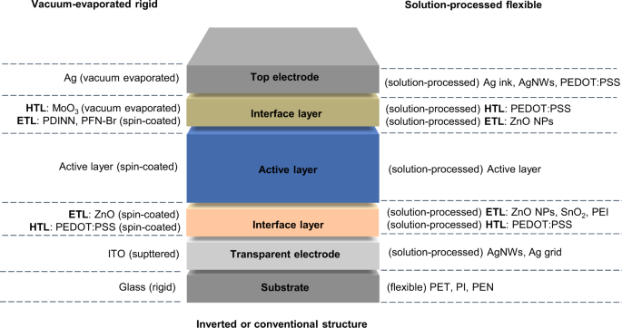
Typical device structure and materials of the OPV prepared by vacuum-evaporated and solution-processed methods.
-
(2)
Combine with large-scale printing technology. Printing technology that can be combined with large-scale production should be introduced into the fabrication process of the device because most layers require solution processing in a solution-processed flexible device. Techniques such as blade coating, spray coating, screen printing, slot-die coating, and inkjet printing have been applied successfully to fabricate OPV101. These printing techniques have been discussed and described earlier in a few reviews and would not be discussed here69,100.
-
(3)
Appropriate solvents of functional layers. In solution-processed devices, the functional layer is obtained from a solution. In addition, the solvents should be screened to prevent dissolution and interpenetration between the functional layers and ineffective film formation. First, the solvents between the two functional layers should be orthogonal. For example, high-efficiency organic active layers are deposited by dissolving polymers or small molecules in organic solvents such as chlorobenzene (CB), chloroform (CF), and toluene. Therefore, the interface layer materials should have good resistance to organic solvents. This limits the suitable options of interface layer materials102. Second, it is necessary to control the solvent evaporation rate to obtain a large-area uniform film. Excessive fast or slow evaporation rates can result in ineffective morphology or a strong coffee ring effect during the expanded production process103. For example, methanol has a low boiling point of 64.7 °C. A few researchers generally use dynamic spin-coating and a high-speed process to reduce the contact time between methanol and the poly3, 4-ethylenedioxythiophene:polystyrene sulfonic acid (PEDOT:PSS) underneath, and obtain a more uniform film104. However, such a dynamic spinning process is not appropriate for mass production.
-
(4)
Good wetting capability. This requirement of orthogonal solvent between functional layers generally introduces another important problem, namely, wetting issues. A solution needs to have good wettability on the surface of the underlying layer to obtain a uniform and complete film using a solution-processing method. For example, PEDOT:PSS is a widely used solution-processed hole-transport layer and an electrode in printable organic photovoltaics. However, its water solubility makes it challenging to deposit directly on the surface of the hydrophobic active layer challenging. Adding a surfactant is an effective strategy to reduce the ink surface tension and improving the wettability of PEDOT:PSS solutions105.
-
(5)
Stable interface. After constructing solution-processed flexible devices, it is necessary to ensure a stable interface between functional layers. Unfavorable physical and chemical reactions between the interfaces should be prevented. In particular, interfacial reactions occur after introducing a high-efficiency active layer. This results in the loss of device efficiency and stability.

Solution-processed electrodes
Solution-processed electrodes are required urgently to fabricate flexible OPV for large-scale production because of their high throughput and low cost. The solution-processed electrodes should satisfy the following requirements for different device applications: (1) High electrical conductivity. Both top and bottom electrodes in the device require high conductivity to reduce the series resistance (Rs) of the device. In particular, in large-area devices, high sheet resistance can significantly reduce the fill factor of the device106. (2) High optical transmittance. To achieve better absorption and improve the photocurrent, transparent electrodes are required to have good transmittance in the visible light range (400–1000 nm). This is because of the better light-absorption properties of the active-layer system107. However, there is a trade-off between the conductivity and optical transmittance of transparent electrodes. Therefore, the figure of merit (FoM) was introduced to evaluate the quality of the transparent electrodes108. (3) Uniformity. For the bottom electrodes, uniformity plays an important role in the achievement of a high fabrication yield and good device performance. Owing to the multilayer-stacked structure of OPV, the high roughness of the bottom electrode directly affects the uniformity and morphology of the upper layers and causes a severe short circuit109. (4) Good solution processability. Electrodes can be deposited by various printing and coating techniques. Conducting polymers, metal nanowires, and metal grids are potential candidates for solution-processed electrodes108.
For bottom transparent electrodes, Magnetron-sputtering metal oxide electrodes such as indium tin oxide (ITO) are used to prepare OPV in the laboratory. Although this type of electrode has remarkable photoelectric properties (the square resistance is approximately 10 Ω sq−1 when the light transmittance is 88%), it has a high energy consumption and low material utilization in the preparation process. Meanwhile, the extensive use of rare metals such as indium further increases the preparation cost110.
Conducting polymers are a type of transparent electrodes prepared by the solution method. Among these, PEDOT:PSS is the most widely used. It displays good solution processing and mechanical flexibility111. Song et al. fabricated flexible ITO-free OPV by all-solution processing at low temperatures98. Figure 4 shows the device structure of a flexible OPV based on PEDOT:PSS electrodes. Treatment with methanesulfonic acid at room temperature prevented damage to the flexible plastic substrates. The devices showed good flexibility and retained ~ 94% of their initial PCE after 1000 bending cycles. However, most post-treatment PEDOT:PSS electrodes used in OPV devices display a low conductivity (<3000 S cm−1) that differs significantly from that of commercial ITO or metal electrodes111,112. This aspect is more critical for large-area devices because it causes increased series resistance and reduces the performance of the devices. In addition, the acidity and hygroscopicity of PEDOT:PSS adversely affect the long-term stability of OPV. Furthermore, strong absorption at long wavelengths can also reduce the photocurrent of the devices.

The requirements and candidates of the solution-processed electrodes in all-solution processed flexible OPV. Reproduced from ref. 116. with permission from the Royal Society of Chemistry.
Metal nanowires such as silver nanowires (AgNWs) are widely used in solution-processed flexible OPV113. However, the large surface roughness of AgNWs can cause severe short circuits in devices because the networks of AgNWs can conveniently penetrate the thin active layer114. The embedment of the AgNW network into the substrate and flattening of the AgNW surface by applying an additional layer are the two primary methods for solving this problem115. For example, Dong et al.116 reported a flexible bottom electrode obtained by embedding AgNWs into polyimide (PI) substrates. The surface roughness (root mean square (RMS)) of the AgNW electrodes decreased to 1.5 nm. The random alignment of AgNWs hinders the balancing of the transmission and square resistance during preparation. Sun et al.117 used water-processed AgNWs to prepare a highly ordered AgNW network structure owing to ionic electrostatic charge repulsion. In water-processed AgNWs, poly(sodium 4-styrenesulfonate) (PSSNa) was added to the AgNW solution as a polyelectrolyte. The films prepared with PSSNa exhibited a more regular arrangement than those prepared without PSSNa. Using this electrode, the flexible OPV achieved an efficiency of 16.5% with a tandem device structure. Zeng et al.118 developed a controllable reduction and chemical welding strategy to improve the conductivity of the AgNW electrode. The fabricated AgNW electrode exhibited a low sheet resistance of 12 Ω sq−1 and high transmittance of 95% at 550 nm. A flexible OPV with a PCE of 17.52% was obtained using this strategy.
Metal grids such as Ag grids are also widely used in large-area OPV owing to their low sheet resistances. Jiang et al. reported the fabrication of printed transparent Ag mesh electrodes by reverse-offset printing119. The printed flexible electrode can achieve both high conductivity and remarkable mechanical durability through effective control. The electrodes displayed 17 Ω sq−1 Rsh at a transmittance of 93.2%, thereby surpassing the performance of the sputtered ITO. Ultrathin OPV with a PCE of 8.3% were prepared using the Ag mesh electrodes printed.
For top electrodes, These differ from bottom solution-processed electrodes. Two important factors should be considered when the top electrode is deposited by the solution method: First, the prepared layers should not be damaged when the top electrode is deposited. Unlike vacuum-evaporated metal electrodes, solution-processed electrodes generally require harsh post-treatment conditions such as high-temperature annealing and penetrating other layers120. Second, high reflectivity. The thickness of the organic photoactive layer is generally 100 nm because of the short exciton diffusion length of the organic photoactive layer material. This prevents sunlight from being absorbed completely when it shines on the active layer. Commonly used vacuum-evaporated electrodes such as silver have good reflectivity. This enables the active layer to absorb secondary light and thereby, increases the photocurrent. However, conventional solution-processed electrodes such as AgNWs and PEDOT:PSS have high transmittance121. Recently, He et al.122 used Ag nanoparticles as the top electrodes. They introduced a hydrogen-intercalated molybdenum oxide (HMO) layer to induce the formation of a smooth solution-processed Ag film. Furthermore, there was no heating or other harsh treatment. However, this process cannot be applied to flexible devices.
Liquid metals such as eutectic gallium–indium (EGaIn) show high conductivity and opacity123. More importantly, the liquid state of EGaIn at room temperature allows for solution processing by spray coating, etc124. Wang et al. dropped EGaIn directly on the surface of active layer in an N2-glovebox125. Pure EGaIn can form a clear and uniform interface without penetration or voids. The ETL would no longer be required in this device because of the matching energy level of pure EGaIn and non-fullerene acceptors. The all-solution-processed devices achieved performance comparable to that of the evaporated reference.
Bihar et al. developed a metal-free device structure with PEDOT:PSS electrodes to achieve all-solution processed flexible OPV126. The PEDOT:PSS electrodes were used as both bottom and top electrodes by inkjet printing. In this work, PEDOT:PSS was treated using various methods to improve processability and device performance. Finally, a fully inkjet-printed ultrathin OPV with a PCE of 3.6% was fabricated successfully. It showed high power-per-weight values and good stability in moist environments.
Solution-processed interface layers
The first and most important requirement of a solution-processed interface layer is the matched energy level (Fig. 5a). Interface layers with suitable energy levels were introduced between the electrodes and active layers to improve charge extraction. The narrow bandgap small-molecule acceptor materials generally have lower HOMO energy levels. These pose new challenges to conventional interface layer materials. Second, the solution-processed interface layers should be robust to protect the active layers from penetration by the solution-processed electrodes. Various interface layers including electron and hole transport layers have been used widely in solution-processed fullerene-based OPV127. However, unlike conventional fullerene-based acceptors, high-efficiency narrow bandgap small-molecules acceptors have more complex chemical structures, e.g., ITIC, IT-4F, and Y6128. These display different chemical activities at the interface129.
Electron transport layer
Sol-gel ZnO and ZnO nanoparticle solutions have been introduced successfully into solution-processed fullerene-based OPV owing to their good solution processability and matched energy levels130. However, in 2019, Jiang et al.131. reported a photocatalytic reaction between ZnO and a non-fullerene acceptor (IT-4F) under UV illumination. Mass spectrometry (MS) and Fourier transform infrared (FT-IR) measurements showed that the chemical structure of IT-4F was destroyed owing to the photocatalytic activity of the ZnO film. The unstable interface between ZnO and non-fullerene acceptors restricts the performance and stability of these cells. The authors replaced ZnO with SnO2, which has been reported to be an effective ETL in perovskite solar cells. The wide bandgap of SnO2 causes the device to display higher performance and photostability than ZnO. They also fabricated 1 cm2 OPV device with a slot-die-coated SnO2 layer. SnO2 also exhibited remarkable thickness tolerance. Bai et al.132 fabricated OPV based on PM6:Y6 by increasing the thickness of the SnO2 films from 10 nm to 160 nm. The PCEs of the cells range from 16.10% to 13.07%. It is noteworthy that the efficiency of the devices remained at 12% with a 530 nm thick blade-coated SnO2 layer. Recently, Hoff et al. successfully deposited SnO2 nanoparticles (NPs) on top of the active layers in air by slot-die coating133. Ethanol was added to a commercial SnO2 solution to improve the film quality. To evaluate the suitability of SnO2 NPs as solution-processed ETL, the device based FBT:PC61BM and PTQ10:IDIC active layers with a conventional device structure ITO/PEDOT:PSS/FBT:PC61BM/SnO2 NPs/Ag were fabricated. All the devices showed significantly higher performance than the devices without ETL. Then, all the slot-die-coated flexible OPV with PET/ITO substrates was fabricated. The interface and active layers were coated sequentially onto the electrodes.
Polyethylenimine (PEI) is a successful polymer-containing amine group for reducing the work functions of various electrodes134. In a previous report, PEI was introduced successfully into fullerene-based blends and assembled at the bottom of the blends135. Lee et al. printed PEI and BHJ simultaneously by blade coating and achieved vertical self-organization of the interface layer136. This new printing method yielded simple tandem OPV devices with four printed layers. However, the amine-containing PEI tends to react with high-efficiency acceptors137,138. Qin et al.19 developed a novel interlayer of Zn2+-chelated polyethylenimine (PEI-Zn) to prevent the reaction between PEI and high-efficiency active layers (Fig. 5b). The chemical reaction activity of PEI was suppressed by chelation of Zn2+ with the PEI. The interlayer exhibits a lower work function and higher conductivity than those of conventional ZnO. They fabricated ultraflexible OPV-based PEDOT:PSS and AgNWs electrodes using PEI-Zn. In addition, PEI-Zn exhibits higher mechanical flexibility than ZnO. It is evident that no cracks appeared on the PEI-Zn film. However, a few cracks appeared after the bending tests. These cracks increased the resistance of the ZnO films. The PEI-Zn film exhibited a more robust bending resistance when the bending radius was <5 mm. We fabricated ultraflexible OPV with different electrodes and interlayers to further evaluate the mechanical flexibility of the interlayers. PEI-Zn-based devices also exhibit higher mechanical flexibility than ZnO-based devices after the continuous deformation cycling test. Compared with metal oxide interlayers, polymer-based interlayers can satisfy the requirements of flexible devices.
Hole transport layer
To achieve solution-processed OPV, silver ink and nanowires used as top electrodes would permeate the layer underneath and reduce the performance. It is necessary to construct a robust interlayer to prevent infiltration of the top electrodes. For an inverted-structure OPV, the hole-transport layers should perform such roles. PEDOT:PSS is a practical material owing to its solution processability, good film-forming capability, and high work function. There have been a series of reports on using PEDOT:PSS as the HTL on top of devices to achieve good performance in solution-processed OPV139,140,141. However, certain problems that occur while depositing PEDOT:PSS films remain to be solved.
The most important problem is the wettability of the aqueous PEDOT:PSS solution deposited on the surface of the active layer. Li et al.105. reported a nonionic surfactant (PEG-TmDD) that enhanced the conductivity and wettability of PEDOT:PSS. The vacuum-free cells based on P3HT:ICBA with the PEDOT:PSS (PH1000 mixed with 4 wt% PEG-TmDD) electrode exhibited good performance, with an FF of 0.6 and PCE of 4.1%. Maisch et al.142 introduced an effective strategy for preparing PEDOT:PSS films on top of the active layer without additives. They improved the wettability of the PEDOT:PSS solution by placing pinning centers on the active-layer film via inkjet printing. This method produced a homogeneous PEDOT:PSS layer on the active layer (P3HT:O-IDTBR) in devices with the structure of ITO/SnO2/P3HT:O-IDTBR/PEDOT:PSS/Ag. It showed performance comparable to those of the reference ones. Recently, Jiang et al.143 synthesized an alcohol-dispersed conducting polymer complex (PEDOT:F). The perfluorinated sulfonic acid (PFSA) ionomers replaced the poly(styrenesulfonic acid) (PSS) counterion during PEDOT polymerization. The produced PEDOT:F formulations can be dispersed both in alcohols and water owing to the special soluble behavior of PFSA. This enables good solution processability on the surface of the organic active layer.
However, the chemical activity of PEDOT:PSS is also problematic. We have mentioned earlier that Zhou and their co-workers determined that the acid of PEDOT:PSS would cause a chemical reaction between PEDOT:PSS and additives in the active layer such as DIO92. This chemical reduction of the PEDOT:PSS resulted in low performance of the devices. Wang et al.144 also reported vertical phase separation in a non-fullerene BHJ system based on PBDB-T:ITIC. After the aging test, the vertical stratification of the PBDB-T:ITIC BHJ was investigated by X-ray photoelectron spectroscopy (XPS) measurements. The results showed that PBDB-T was enriched at the upper surface and that ITIC was enriched at the bottom surface of the BHJ. The Raman spectra show an apparent shift in the quinoidal PEDOT configuration on the PEDOT:PSS/ITIC surface compared with the pristine PEDOT:PSS surface. This shift was attributed to the chemical reaction between ITIC and PEDOT:PSS.

a The requirements and b solved strategies of the solution-processed interface layer in solution-processed flexible OPV. Reproduced from ref. 131. with permission from the Royal Society of Chemistry.
Another issue with the use of PEDOT: PSS as an HTL in OPV is the mismatch in energy level. The high-efficiency acceptors such as Y6 and IT-4F have deep HOMO of -5.62 and -5.71 eV, respectively145. The polymer PM6 containing a F substitution with a HOMO of -5.54 eV is generally selected as a donor to match the energy level. However, the Fermi level of PEDOT:PSS was significantly higher than that of PM6. This large gap in energy level (~0.5 eV) between the donor and PEDOT:PSS causes severe charge extraction. Han et al.146. reported a reduction in the VOC of the OPV owing to the mismatch in energy level between the HTL solar cell and the polymer donor. A bilayer HTL structure (WO3/PEDOT:PSS) was introduced into a printed OPV for VOC recovery to solve this issue. The work function of the bilayer HTLs (-5.27 eV) is significantly closer to the HOMO of the donor (SMD2; −5.44 eV) than that of the HTL solar (−5.05 eV). Significant improvements in device performance can be achieved using JSC, VOC, and FF. The bilayer HTL structure can also enhance the photostability of the devices under UV light. Flexible OPV modules containing 10 subcells were fabricated by slot-die coating and screen printing owing to the high solution processability of bilayer HTLs. The device exhibited a PCE of 5.25% with an active area of 80 cm2. Sun et al. observed a similar phenomenon of reduction in Voc when they fabricated all-solution-processed OPV using PEDOT:PSS PH1000 as the printable electrode and PM6:Y6:IDIC as the active layer39. The researchers attributed the decrease in performance to physical and chemical compatibility issues between the active layer and polymer electrodes. Therefore, solution-processed HxMoO3 was employed to solve the issues of hole extraction and wetting between the high-efficiency active layer and PEDOT:PSS. Compared with PEDOT:PSS, the deeper Fermi level of HxMoO3 (-5.44 eV) enhanced charge extraction in the devices. The solution-processed HxMoO3 had good wettability on the surface of the active layer because of the ethanol solvent. Most importantly, the hydrophilic surface of HxMoO3 facilitated the deposition of PEDOT:PSS on top of it. The HxMoO3 composition was controlled finely by tuning the reaction conditions to obtain processing orthogonality between HxMoO3 and PEDOT:PSS. With the introduction of the HxMoO3 layer, the flexible all-solution processed OPV (all the layers from the bottom substrate to the top electrode) were fabricated effectively with an efficiency of 11.9% for small-area devices (0.04 cm2) and 10.3% for 1 cm2 devices. The emerging high-performance non-fullerene acceptors (such as Y6) were adopted successfully in all-solution processed OPV device.
Summary and outlook
This review summarizes the recent work on solution-processed flexible OPV. Large-scale printing is a prerequisite for the commercial application of OPV. The efficiency of OPV has been a significant breakthrough in the laboratory with the rapid development of narrow bandgap small-molecule acceptor and wide bandgap polymer donor materials. Researchers need to consider how to translate lab cells into commercial cells using the printing process. In this review, we presented and evaluated studies on solution-processed flexible OPV in terms of various aspects, including the solution process requirements and different solution-processed functional layers.
Although many researchers have reported remarkable work on solution-processed flexible OPV, the following aspects need to be examined further for commercial applications.
-
(1)
Stability of the OPV. The efficiency of OPV is higher (>19%) than the market viability that is generally assumed (15%). Stability is the main limitation that needs to be examined in commercial applications. Loo et al.147 recently published a comment in the journal Nature Energy to induce researchers to pay more attention to the material stability and device longevity of OPV. The complex chemical structure of the active layer materials can generate more unstable factors in solution-processed OPV devices. The next step in the development of OPV should focus on enhancing the stability of the devices. Developing more stable materials and robust device structures is an effective strategy.
-
(2)
Thicker and less expensive active layers. The high-efficiency OPV reported in the literature is mostly fabricated in the laboratory by spin coating with a film thickness of ~100 nm. Such a small film thickness causes issues in printing large-area OPV. Thin films are susceptible to defects on the substrates. However, it is difficult to homogenously control such thin films during large-scale fabrication. Thick active layers (> 300 nm) can be better matched for roll-to-roll large-scale printing and enhance photon harvesting. A few groups have reported OPV based on the printed thick-high-efficiency active layer with remarkable PCE148,149. However, the efficiency of these devices with thick active layers differs significantly from the highest reported efficiency. The low charge carrier mobility and charge carrier recombination decrease the device performance with improved thickness of the active layer. This limits the number of materials suitable for thicker layers. Therefore, the development of a high-efficiency active layer with thickness tolerability is desirable. The cost of high-efficiency active layer materials also needs to be reduced further to satisfy the demand for the scale test of printed OPV in the laboratory150.
-
(3)
Simple device structure. The reported high-efficiency OPV typically have a multilayer structure (more than five layers). A larger number of layers implies a larger number of interfaces. This multilayer structure has high requirements for the interface layer. Interlayers need to be stable, convenient to process, and sufficiently robust to prevent penetration from the deposition of the upper layer. This complex interface would hinder large-scale production because a few of the interface layers have a size of only several nanometers. Therefore, it is highly important to develop a simple device structure while maintaining device performance, for large-scale production.
To summarize, the development of high-efficiency active layer materials has further promoted the large-scale production of OPV. However, it also introduces new challenges. The preparation of high-efficiency and stable solution-processed flexible OPV requires more extensive research on the interface, printing methods, and materials development. We consider that this review would inspire readers to promote the commercialization of OPV.
Data availability
All data are available in the main text.
References
Li, G., Zhu, R. & Yang, Y. Polymer solar cells. Nat. Photon. 6, 153–161 (2012).
Günes, S., Neugebauer, H. & Sariciftci, N. S. Conjugated polymer-based organic solar cells. Chem. Rev. 107, 1324–1338 (2007).
Tang, C. W. Two-layer organic photovoltaic cell. Appl. Phys. Lett. 48, 183–185 (1986).
Cui, Y. et al. Single-junction organic photovoltaic cells with approaching 18% efficiency. Adv. Mater. 32, 1908205 (2020).
Zhan, L. et al. Over 17% efficiency ternary organic solar cells enabled by two non-fullerene acceptors working in an alloy-like model. Energy Environ. Sci. 13, 635–645 (2020).
Zhan, L. et al. Desired open-circuit voltage increase enables efficiencies approaching 19% in symmetric-asymmetric molecule ternary organic photovoltaics. Joule 6, 662–675 (2022).
Zhu, L. et al. Single-junction organic solar cells with over 19% efficiency enabled by a refined double-fibril network morphology. Nat. Mater. 21, 656–663 (2022).
Zhao, F. et al. Single-junction binary-blend nonfullerene polymer solar cells with 12.1% efficiency. Adv. Mater. 29, 1700144 (2017).
Zhao, W. et al. Fullerene-free polymer solar cells with over 11% efficiency and excellent thermal stability. Adv. Mater. 28, 4734–4739 (2016).
Mao, L. et al. Writable and patternable organic solar cells and modules inspired by an old chinese calligraphy tradition. Mater. Horiz. 5, 123–130 (2018).
Yuan, J. et al. Single-junction organic solar cell with over 15% efficiency using fused-ring acceptor with electron-deficient core. Joule 3, 1140–1151 (2019).
Wang, W. et al. Fused hexacyclic nonfullerene acceptor with strong near-infrared absorption for semitransparent organic solar cells with 9.77% efficiency. Adv. Mater. 29, 1701308 (2017).
Dennler, G., Scharber, M. C. & Brabec, C. J. Polymer-fullerene bulk-heterojunction solar cells. Adv. Mater. 21, 1323–1338 (2009).
Li, S. et al. Efficient organic solar cells with non-fullerene acceptors. Small 13, 1701120 (2017).
Cui, Y. et al. Wide-gap non-fullerene acceptor enabling high-performance organic photovoltaic cells for indoor applications. Nat. Energy 4, 768–775 (2019).
Wang, Y. et al. Recent progress and challenges toward highly stable nonfullerene acceptor-based organic solar cells. Adv. Energy Mater. 11, 2003002 (2021).
Dai, S. & Zhan, X. Nonfullerene acceptors for semitransparent organic solar cells. Adv. Energy Mater. 8, 1800002 (2018).
Lipomi, D. J., Tee, B. C.-K., Vosgueritchian, M. & Bao, Z. Stretchable organic solar cells. Adv. Mater. 23, 1771–1775 (2011).
Qin, F. et al. Robust metal ion-chelated polymer interfacial layer for ultraflexible non-fullerene organic solar cells. Nat. Commun. 11, 4508 (2020).
Kaltenbrunner, M. et al. Ultrathin and lightweight organic solar cells with high flexibility. Nat. Commun. 3, 770 (2012).
Jinno, H. et al. Stretchable and waterproof elastomer-coated organic photovoltaics for washable electronic textile applications. Nat. Energy 2, 780–785 (2017).
Gaynor, W., Lee, J.-Y. & Peumans, P. Fully solution-processed inverted polymer solar cells with laminated nanowire electrodes. ACS Nano 4, 30–34 (2010).
Yim, J. H. et al. Fully solution-processed semitransparent organic solar cells with a silver nanowire cathode and a conducting polymer anode. ACS Nano 8, 2857–2863 (2014).
Brabec, C. J. & Durrant, J. R. Solution-processed organic solar cells. MRS Bull. 33, 670–675 (2011).
Krebs, F. C., Gevorgyan, S. A. & Alstrup, J. A roll-to-roll process to flexible polymer solar cells: model studies, manufacture and operational stability studies. J. Mater. Chem. 19, 5442–5451 (2009).
Berny, S. et al. Solar trees: first large-scale demonstration of fully solution coated, semitransparent, flexible organic photovoltaic modules. Adv. Sci. 3, 1500342 (2016).
Gu, X. et al. Roll-to-roll printed large-area all-polymer solar cells with 5% efficiency based on a low crystallinity conjugated polymer blend. Adv. Energy Mater. 7, 1602742 (2017).
Jung, S. et al. All-inkjet-printed, all-air-processed solar cells. Adv. Energy Mater. 4, 1400432 (2014).
Angmo, D. et al. Roll-to-roll printed silver nanowire semitransparent electrodes for fully ambient solution-processed tandem polymer solar cells. Adv. Funct. Mater. 25, 4539–4547 (2015).
Krebs, F. C. All solution roll-to-roll processed polymer solar cells free from indium-tin-oxide and vacuum coating steps. Org. Electron. 10, 761–768 (2009).
Hong, S. et al. Effect of solvent on large-area polymer-fullerene solar cells fabricated by a slot-die coating method. Sol. Energy Mater. Sol. Cells 126, 107–112 (2014).
Carlé, J. E. et al. Upscaling from single cells to modules-fabrication of vacuum- and ito-free polymer solar cells on flexible substrates with long lifetime. J. Mater. Chem. C 2, 1290–1297 (2014).
Krebs, F. C., Tromholt, T. & Jorgensen, M. Upscaling of polymer solar cell fabrication using full roll-to-roll processing. Nanoscale 2, 873–886 (2010).
Guo, F. et al. Fully printed organic tandem solar cells using solution-processed silver nanowires and opaque silver as charge collecting electrodes. Energy Environ. Sci. 8, 1690–1697 (2015).
Fu, Y., Huang, Y., Li, Y. & Li, Y. Large-area flexible organic solar cells. npj Flex. Electron. 5, 30 (2021).
Li, Y., Xu, G., Cui, C. & Li, Y. Flexible and semitransparent organic solar cells. Adv. Energy Mater. 8, 1701791 (2018).
Chen, X. et al. Realizing ultrahigh mechanical flexibility and >15% efficiency of flexible organic solar cells via a “welding” flexible transparent electrode. Adv. Mater. 32, 1908478 (2020).
Zeng, G. et al. Breaking 12% efficiency in flexible organic solar cells by using a composite electrode. Sci. China Chem. 62, 851–858 (2019).
Sun, L. et al. Flexible all-solution-processed organic solar cells with high-performance nonfullerene active layers. Adv. Mater. 32, 1907840 (2020).
Sorrentino, R., Kozma, E., Luzzati, S. & Po, R. Interlayers for non-fullerene based polymer solar cells: distinctive features and challenges. Energy Environ. Sci. 14, 180–223 (2021).
Fan, J.-Y. et al. High-performance organic solar modules via the bilayer-merged-annealing assisted blading coating. Adv. Mater. 34, 2110569 (2022).
Ro, H. W. et al. Morphology changes upon scaling a high-efficiency, solution-processed solar cell. Energy Environ. Sci. 9, 2835–2846 (2016).
Scharber, M. C. & Sariciftci, N. S. Efficiency of bulk-heterojunction organic solar cells. Prog. Polym. Sci. 38, 1929–1940 (2013).
Dang, M. T., Hirsch, L. & Wantz, G. P3ht:Pcbm, best seller in polymer photovoltaic research. Adv. Mater. 23, 3597–3602 (2011).
Miller, S. et al. Investigation of nanoscale morphological changes in organic photovoltaics during solvent vapor annealing. J. Mater. Chem. 18, 306–312 (2008).
Ma, W. et al. Thermally stable, efficient polymer solar cells with nanoscale control of the interpenetrating network morphology. Adv. Funct. Mater. 15, 1617–1622 (2005).
Zhao, G., He, Y. & Li, Y. 6.5% efficiency of polymer solar cells based on poly(3-hexylthiophene) and indene-c60 bisadduct by device optimization. Adv. Mater. 22, 4355–4358 (2010).
Zhang, M. et al. A polythiophene derivative with superior properties for practical application in polymer solar cells. Adv. Mater. 26, 5880–5885 (2014).
He, Z. et al. Single-junction polymer solar cells with high efficiency and photovoltage. Nat. Photon. 9, 174–179 (2015).
Sun, R. et al. Single-junction organic solar cells with 19.17% efficiency enabled by introducing one asymmetric guest acceptor. Adv. Mater. 34, 2110147 (2022).
Armin, A. et al. A history and perspective of non-fullerene electron acceptors for organic solar cells. Adv. Energy Mater. 11, 2003570 (2021).
Lin, Y. et al. An electron acceptor challenging fullerenes for efficient polymer solar cells. Adv. Mater. 27, 1170–1174 (2015).
Gao, L. et al. High-efficiency nonfullerene polymer solar cells with medium bandgap polymer donor and narrow bandgap organic semiconductor acceptor. Adv. Mater. 28, 8288–8295 (2016).
Li, S., Li, C.-Z., Shi, M. & Chen, H. New phase for organic solar cell research: emergence of y-series electron acceptors and their perspectives. ACS Energy Lett. 5, 1554–1567 (2020).
Liu, J. et al. Fast charge separation in a non-fullerene organic solar cell with a small driving force. Nat. Energy 1, 16089 (2016).
Liu, Q. et al. 18% efficiency organic solar cells. Sci. Bull. 65, 272–275 (2020).
Zhang, S., Qin, Y., Zhu, J. & Hou, J. Over 14% efficiency in polymer solar cells enabled by a chlorinated polymer donor. Adv. Mater. 30, 1800868 (2018).
Fu, H., Wang, Z. & Sun, Y. Polymer donors for high-performance non-fullerene organic solar cells. Angew. Chem. Int. Ed. 58, 4442–4453 (2019).
Qian, D. et al. Design, application, and morphology study of a new photovoltaic polymer with strong aggregation in solution state. Macromolecules 45, 9611–9617 (2012).
Zhao, W. et al. Molecular optimization enables over 13% efficiency in organic solar cells. J. Am. Chem. Soc. 139, 7148–7151 (2017).
Li, W. et al. A high-efficiency organic solar cell enabled by the strong intramolecular electron push–pull effect of the nonfullerene acceptor. Adv. Mater. 30, 1707170 (2018).
Jiang, K. et al. Alkyl chain tuning of small molecule acceptors for efficient organic solar cells. Joule 3, 3020–3033 (2019).
Dong, X. et al. Large-area organic solar modules with efficiency over 14%. Adv. Funct. Mater. 32, 2110209 (2022).
Zhang, S., Ye, L., Zhang, H. & Hou, J. Green-solvent-processable organic solar cells. Mater. Today 19, 533–543 (2016).
Huang, H. et al. Green solvent-processed organic solar cells based on a low cost polymer donor and a small molecule acceptor. J. Mater. Chem. C 8, 7718–7724 (2020).
Wan, J. et al. All-green solvent-processed planar heterojunction organic solar cells with outstanding power conversion efficiency of 16%. Adv. Funct. Mater. 32, 2107567 (2022).
Chen, H. et al. A guest-assisted molecular-organization approach for >17% efficiency organic solar cells using environmentally friendly solvents. Nat. Energy 6, 1045–1053 (2021).
Søndergaard, R. R., Hösel, M. & Krebs, F. C. Roll-to-roll fabrication of large area functional organic materials. J. Polym. Sci. Polym. Phys. 51, 16–34 (2013).
Sampaio, P. G. V. et al. Overview of printing and coating techniques in the production of organic photovoltaic cells. Int. J. Energy Res. 44, 9912–9931 (2020).
Zimmermann, B., Schleiermacher, H. F., Niggemann, M. & Würfel, U. Ito-free flexible inverted organic solar cell modules with high fill factor prepared by slot die coating. Sol. Energy Mater. Sol. Cells 95, 1587–1589 (2011).
Larsen-Olsen, T. T. et al. Simultaneous multilayer formation of the polymer solar cell stack using roll-to-roll double slot-die coating from water. Sol. Energy Mater. Sol. Cells 97, 22–27 (2012).
Pérez-Gutiérrez, E. et al. Organic solar cells all made by blade and slot–die coating techniques. Sol. Energy 146, 79–84 (2017).
Lee, J. et al. Slot-die and roll-to-roll processed single junction organic photovoltaic cells with the highest efficiency. Adv. Energy Mater. 9, 1901805 (2019).
Aziz, F. & Ismail, A. F. Spray coating methods for polymer solar cells fabrication: a review. Mater. Sci. Semicond. Process. 39, 416–425 (2015).
Huang, Y. et al. All-spray-coated inverted semitransparent organic solar cells and modules. IEEE J. Photovolt. 8, 144–150 (2018).
Arumugam, S. et al. Solution processed organic solar cells on textiles. IEEE J. Photovolt. 8, 1710–1715 (2018).
Kang, M. H. et al. Fabrication of spray-coated semitransparent organic solar cells. IEEE J. Electron Dev. Soc. 7, 1129–1132 (2019).
Arumugam, S. et al. Fully spray-coated organic solar cells on woven polyester cotton fabrics for wearable energy harvesting applications. J. Mater. Chem. A 4, 5561–5568 (2016).
La Notte, L. et al. Sprayed organic photovoltaic cells and mini-modules based on chemical vapor deposited graphene as transparent conductive electrode. Carbon 129, 878–883 (2018).
Peng, X. et al. Perovskite and organic solar cells fabricated by inkjet printing: Progress and prospects. Adv. Funct. Mater. 27, 1703704 (2017).
Angmo, D. et al. Inkjet printing of back electrodes for inverted polymer solar cells. Adv. Energy Mater. 3, 1230–1237 (2013).
Eggenhuisen, T. M. et al. High efficiency, fully inkjet printed organic solar cells with freedom of design. J. Mater. Chem. A 3, 7255–7262 (2015).
Corzo, D. et al. Digital inkjet printing of high-efficiency large-area nonfullerene organic solar cells. Adv. Mater. Technol. 4, 1900040 (2019).
Zhong, M. et al. Soft porous blade printing of nonfullerene organic solar cells. ACS Appl. Mater. Interfaces 12, 25843–25852 (2020).
Sun, L., Jiang, X. & Zhou, Y. Efficient nonfullerene organic solar cells with active layers fabricated by water transfer printing. J. Energy Chem. 37, 220–224 (2019).
Zhu, L. et al. Efficient organic solar cell with 16.88% efficiency enabled by refined acceptor crystallization and morphology with improved charge transfer and transport properties. Adv. Energy Mater. 10, 1904234 (2020).
Zhao, F., Wang, C. & Zhan, X. Morphology control in organic solar cells. Adv. Energy Mater. 8, 1703147 (2018).
Maeda, A. et al. Photoactive layer formation in the dark for high performance of air-processable organic photovoltaics. J. Phys. Mater. 4, 044016 (2021).
Lin, Y. et al. Printed nonfullerene organic solar cells with the highest efficiency of 9.5%. Adv. Energy Mater. 8, 1701942 (2018).
Zhang, L. et al. Blade-coated efficient and stable large-area organic solar cells with optimized additive. Org. Electron. 83, 105771 (2020).
Tremolet de Villers, B. J. et al. Removal of residual diiodooctane improves photostability of high-performance organic solar cell polymers. Chem. Mater. 28, 876–884 (2016).
Wang, W. et al. Exploring the chemical interaction between diiodooctane and pedot-pss electrode for metal electrode-free nonfullerene organic solar cells. ACS Appl. Mater. Interfaces 12, 3800–3805 (2020).
Song, S. et al. Hot slot die coating for additive-free fabrication of high performance roll-to-roll processed polymer solar cells. Energy Environ. Sci. 11, 3248–3255 (2018).
Na, S. I. et al. High performance roll-to-roll produced fullerene-free organic photovoltaic devices via temperature-controlled slot die coating. Adv. Funct. Mater. 29, 1805825 (2019).
Arunagiri, L. et al. Temperature-dependent aggregation donor polymers enable highly efficient sequentially processed organic photovoltaics without the need of orthogonal solvents. Adv. Funct. Mater. 29, 1902478 (2019).
Bernardo, B. et al. Progress in upscaling organic photovoltaic devices. Adv. Energy Mater. 11, 2100342 (2021).
Meng, X. et al. A general approach for lab-to-manufacturing translation on flexible organic solar cells. Adv. Mater. 31, 1903649 (2019).
Song, W. et al. All-solution-processed metal-oxide-free flexible organic solar cells with over 10% efficiency. Adv. Mater. 30, 1800075 (2018).
Cai, M. et al. Cost-performance analysis of perovskite solar modules. Adv. Sci. 4, 1600269 (2017).
Ganesan, S., Mehta, S. & Gupta, D. Fully printed organic solar cells – a review of techniques, challenges and their solutions. Opto-Electron. Rev. 27, 298–320 (2019).
Krebs, F. C. Fabrication and processing of polymer solar cells: a review of printing and coating techniques. Sol. Energy Mater. Sol. Cells 93, 394–412 (2009).
Aizawa, N. et al. Simultaneous cross-linking and p-doping of a polymeric semiconductor film by immersion into a phosphomolybdic acid solution for use in organic solar cells. Chem. Commun. 52, 3825–3827 (2016).
Girotto, C., Moia, D., Rand, B. P. & Heremans, P. High-performance organic solar cells with spray-coated hole-transport and active layers. Adv. Funct. Mater. 21, 64–72 (2011).
Gao, J. et al. One key issue in characterization of organic solar cells with solution processed interfacial layers. Phys. Chem. Chem. Phys. 21, 5790–5795 (2019).
Li, Z. et al. A nonionic surfactant simultaneously enhancing wetting property and electrical conductivity of pedot:pss for vacuum-free organic solar cells. Sol. Energy Mater. Sol. Cells 137, 311–318 (2015).
Choi, S., Potscavage Jr, W. J. & Kippelen, B. Area-scaling of organic solar cells. J. Appl. Phys. 106, 054507 (2009).
Zhang, J. et al. Material insights and challenges for non-fullerene organic solar cells based on small molecular acceptors. Nat. Energy 3, 720–731 (2018).
Zhang, Y., Ng, S.-W., Lu, X. & Zheng, Z. Solution-processed transparent electrodes for emerging thin-film solar cells. Chem. Rev. 4, 2049–2122 (2020).
Dahou, F. Z. et al. Influence of anode roughness and buffer layer nature on organic solar cells performance. Thin Solid Films 518, 6117–6122 (2010).
Emmott, C. J. M., Urbina, A. & Nelson, J. Environmental and economic assessment of ito-free electrodes for organic solar cells. Sol. Energy Mater. Sol. Cells 97, 14–21 (2012).
Jiang, Y., Liu, T. & Zhou, Y. Recent advances of synthesis, properties, film fabrication methods, modifications of poly(3,4-ethylenedioxythiophene), and applications in solution-processed photovoltaics. Adv. Funct. Mater. 30, 2006213 (2020).
Kim, Y. H. et al. Highly conductive pedot:Pss electrode with optimized solvent and thermal post-treatment for ito-free organic solar cells. Adv. Funct. Mater. 21, 1076–1081 (2011).
Basarir, F. et al. Recent progresses on solution-processed silver nanowire based transparent conducting electrodes for organic solar cells. Mater. Today Chem. 3, 60–72 (2017).
Langley, D. et al. Flexible transparent conductive materials based on silver nanowire networks: a review. Nanotechnology 24, 452001 (2013).
Azani, M.-R., Hassanpour, A. & Torres, T. Benefits, problems, and solutions of silver nanowire transparent conductive electrodes in indium tin oxide (ito)-free flexible solar cells. Adv. Energy Mater. 10, 2002536 (2020).
Dong, X. et al. Flexible nonfullerene organic solar cells based on embedded silver nanowires with an efficiency up to 11.6%. J. Mater. Chem. A 7, 1989–1995 (2019).
Sun, Y. et al. Flexible organic photovoltaics based on water-processed silver nanowire electrodes. Nat. Electron. 2, 513–520 (2019).
Zeng, G. et al. Realizing 17.5% efficiency flexible organic solar cells via atomic-level chemical welding of silver nanowire electrodes. J. Am. Chem. Soc. 19, 8658–8668 (2022).
Jiang, Z. et al. Reverse-offset printed ultrathin ag mesh for robust conformal transparent electrodes for high-performance organic photovoltaics. Adv. Mater. 30, 1707526 (2018).
Liu, C., Xiao, C., Xie, C. & Li, W. Flexible organic solar cells: materials, large-area fabrication techniques and potential applications. Nano Energy 89, 106399 (2021).
Hu, Z. et al. A critical review on semitransparent organic solar cells. Nano Energy 78, 105376 (2020).
He, X. et al. Evaporation-free organic solar cells with high efficiency enabled by dry and nonimmersive sintering strategy. Adv. Funct. Mater. 31, 2010764 (2021).
Neumann, T. V. & Dickey, M. D. Liquid metal direct write and 3d printing: a review. Adv. Mater. Technol. 5, 2000070 (2020).
Noh, J. et al. Intrinsically stretchable organic solar cells with efficiencies of over 11%. ACS Energy Lett. 6, 2512–2518 (2021).
Wang, J. et al. Solution-processed electron-transport layer-free organic photovoltaics with liquid metal cathodes. ACS Appl. Mater. Interfaces 14, 14165–14173 (2022).
Bihar, E. et al. Fully inkjet-printed, ultrathin and conformable organic photovoltaics as power source based on cross-linked pedot:pss electrodes. Adv. Mater. Technol. 5, 2000226 (2020).
Steim, R., Kogler, F. R. & Brabec, C. J. Interface materials for organic solar cells. J. Mater. Chem. 20, 2499–2512 (2010).
Hou, J., Inganäs, O., Friend, R. H. & Gao, F. Organic solar cells based on non-fullerene acceptors. Nat. Mater. 17, 119 (2018).
Hu, L. et al. Influence of substituent groups on chemical reactivity kinetics of nonfullerene acceptors. J. Phys. Chem. C 124, 2307–2312 (2020).
Huang, J., Yin, Z. & Zheng, Q. Applications of zno in organic and hybrid solar cells. Energy Environ. Sci. 4, 3861–3877 (2011).
Jiang, Y. et al. Photocatalytic effect of ZnO on the stability of nonfullerene acceptors and its mitigation by SnO2 for nonfullerene organic solar cells. Mater. Horiz. 6, 1438–1443 (2019).
Bai, Y. et al. Printable sno2 cathode interlayer with up to 500 nm thickness-tolerance for high-performance and large-area organic solar cells. Sci. China Chem. 63, 957–965 (2020).
Hoff, A., Farahat, M. E., Pahlevani, M. & Welch, G. C. Tin oxide electron transport layers for air-/solution-processed conventional organic solar cells. ACS Appl. Mater. Interfaces 14, 1568–1577 (2022).
Zhou, Y. et al. A universal method to produce low–work function electrodes for organic electronics. Science 336, 327 (2012).
Kang, H. et al. Simplified tandem polymer solar cells with an ideal self-organized recombination layer. Adv. Mater. 27, 1408–1413 (2015).
Kim, S. et al. A versatile self-organization printing method for simplified tandem organic photovoltaics. Adv. Funct. Mater. 26, 3563–3569 (2016).
Hu, L. et al. Chemical reaction between an itic electron acceptor and an amine-containing interfacial layer in non-fullerene solar cells. J. Mater. Chem. A 6, 2273–2278 (2018).
Xiong, S. et al. 12.5% flexible nonfullerene solar cells by passivating the chemical interaction between the active layer and polymer interfacial layer. Adv. Mater. 31, 1806616 (2019).
Helgesen, M., Carlé, J. E. & Krebs, F. C. Slot-die coating of a high performance copolymer in a readily scalable roll process for polymer solar cells. Adv. Energy Mater. 3, 1664–1669 (2013).
Liu, K. et al. Roll-coating fabrication of flexible organic solar cells: comparison of fullerene and fullerene-free systems. J. Mater. Chem. A 4, 1044–1051 (2016).
Carlé, J. E. et al. A laboratory scale approach to polymer solar cells using one coating/printing machine, flexible substrates, no ito, no vacuum and no spincoating. Sol. Energy Mater. Sol. Cells 108, 126–128 (2013).
Maisch, P. et al. A generic surfactant-free approach to overcome wetting limitations and its application to improve inkjet-printed p3ht:Non-fullerene acceptor pv. J. Mater. Chem. A 7, 13215–13224 (2019).
Jiang, Y. et al. An alcohol-dispersed conducting polymer complex for fully printable organic solar cells with improved stability. Nat. Energy 7, 352–359 (2022).
Wang, Y. et al. Stability of nonfullerene organic solar cells: from built-in potential and interfacial passivation perspectives. Adv. Energy Mater. 9, 1900157 (2019).
Li, K. et al. Ternary blended fullerene-free polymer solar cells with 16.5% efficiency enabled with a higher-lumo-level acceptor to improve film morphology. Adv. Energy Mater. 9, 1901728 (2019).
Han, Y. W. et al. Evaporation-free nonfullerene flexible organic solar cell modules manufactured by an all-solution process. Adv. Energy Mater. 9, 1902065 (2019).
Burlingame, Q., Ball, M. & Loo, Y.-L. It’s time to focus on organic solar cell stability. Nat. Energy 5, 947–949 (2020).
Ma, L. et al. High-efficiency nonfullerene organic solar cells enabled by 1000 nm thick active layers with a low trap-state density. ACS Appl. Mater. Interfaces 12, 18777–18784 (2020).
Wang, G., Adil, M. A., Zhang, J. & Wei, Z. Large-area organic solar cells: Material requirements, modular designs, and printing methods. Adv. Mater. 31, 1805089 (2019).
Xue, R., Zhang, J., Li, Y. & Li, Y. Organic solar cell materials toward commercialization. Small 14, 1801793 (2018).
Mao, Y. et al. Evolution of molecular aggregation in bar-coated non-fullerene organic solar cells. Mater. Chem. Front. 3, 1062–1070 (2019).
Mao, Y. et al. Molecular ordering and performance of ternary nonfullerene organic solar cells via bar-coating in air with an efficiency over 13%. ACS Appl. Mater. Interfaces 11, 35827–35834 (2019).
Kim, H. S. et al. Synthesis of itic derivatives with extended π-conjugation as non-fullerene acceptors for organic solar cells. ACS Appl. Mater. Interfaces 11, 47121–47130 (2019).
Jeong, S. et al. Large-area nonfullerene organic solar cell modules fabricated by a temperature-independent printing method. ACS Appl. Mater. Interfaces 12, 41877–41885 (2020).
Zhu, C. et al. Spin-coated 10.46% and blade-coated 9.52% of ternary semitransparent organic solar cells with 26.56% average visible transmittance. Sol. Energy 204, 660–666 (2020).
Pascual-San-José, E. et al. Towards photovoltaic windows: scalable fabrication of semitransparent modules based on non-fullerene acceptors via laser-patterning. J. Mater. Chem. A 8, 9882 (2020).
Cui, Y. et al. Achieving over 15% efficiency in organic photovoltaic cells via copolymer design. Adv. Mater. 31, 1808356 (2019).
Guo, X. et al. Fully doctor-bladed efficient organic solar cells processed under ambient condition. Org. Electron. 82, 105725 (2020).
Aatif, M. & Tiwari, J. P. Futuristic electron transport layer based on multifunctional interactions of zno/tcne for stable inverted organic solar cells. RSC Adv. 10, 42305–42317 (2020).
Zhao, W. et al. Vacuum-assisted annealing method for high efficiency printable large-area polymer solar cell modules. J. Mater. Chem. C. 7, 3206–3211 (2019).
Zhang, L. et al. A blade-coated highly efficient thick active layer for non-fullerene organic solar cells. J. Mater. Chem. A 7, 22265–22273 (2019).
Lee, S. et al. Achieving thickness-insensitive morphology of the photoactive layer for printable organic photovoltaic cells via side chain engineering in nonfullerene acceptors. Adv. Energy Mater. 9, 1900044 (2019).
Huang, K.-M. et al. Nonfullerene polymer solar cell with large active area of 216 cm2 and high power conversion efficiency of 7.7%. Sol. RRL 3, 1900071 (2019).
Dong, S. et al. Suppressing the excessive aggregation of nonfullerene acceptor in blade-coated active layer by using n-type polymer additive to achieve large-area printed organic solar cells with efficiency over 15%. EcoMat 1, e12006 (2019).
Zhao, W. et al. Environmentally friendly solvent-processed organic solar cells that are highly efficient and adaptable for the blade-coating method. Adv. Mater. 30, 1704837 (2018).
Zhang, L. et al. Blade-cast nonfullerene organic solar cells in air with excellent morphology, efficiency, and stability. Adv. Mater. 30, 1800343 (2018).
Ye, L. et al. Surpassing 10% efficiency benchmark for nonfullerene organic solar cells by scalable coating in air from single nonhalogenated solvent. Adv. Mater. 30, 1705485 (2018).
Strohm, S. et al. P3ht: Non-fullerene acceptor based large area, semi-transparent pv modules with power conversion efficiencies of 5%, processed by industrially scalable methods. Energy Environ. Sci. 11, 2225–2234 (2018).
Chang, K. et al. Efficient non-fullerene organic photovoltaics printed by electrospray via solvent engineering. ACS Appl. Mater. Interfaces 12, 27405–27415 (2020).
Sun, R. et al. A layer-by-layer architecture for printable organic solar cells overcoming the scaling lag of module efficiency. Joule 4, 407–419 (2020).
Wang, Y. et al. Sequential blade-coated acceptor and donor enables simultaneous enhancement of efficiency, stability, and mechanical properties for organic solar cells. Adv. Energy Mater. 10, 1903609 (2020).
Liu, W. et al. Roll-coating fabrication of ito-free flexible solar cells based on a non-fullerene small molecule acceptor. RSC Adv. 5, 36001–36006 (2015).
Arredondo, B. et al. Identification of degradation mechanisms in slot-die-coated nonfullerene ito-free organic solar cells using different illumination spectra. ACS Appl. Energy Mater. 3, 6476–6485 (2020).
Zhao, H. et al. Processing-friendly slot-die-cast nonfullerene organic solar cells with optimized morphology. ACS Appl. Mater. Interfaces 11, 42392–42402 (2019).
Wu, Q. et al. Slot-die printed non-fullerene organic solar cells with the highest efficiency of 12.9% for low-cost pv-driven water splitting. Nano Energy 61, 559–566 (2019).
Wienhold, K. S. et al. Effect of solvent additives on the morphology and device performance of printed nonfullerene acceptor based organic solar cells. ACS Appl. Mater. Interfaces 11, 42313–42321 (2019).
Tintori, F., Laventure, A. & Welch, G. C. Perylene diimide based organic photovoltaics with slot-die coated active layers from halogen-free solvents in air at room temperature. ACS Appl. Mater. Interfaces 11, 39010–39017 (2019).
Destouesse, E. et al. Slot-die processing and encapsulation of non-fullerene based ito-free organic solar cells and modules. Flex. Print. Electron. 4, 045004 (2019).
Acknowledgements
This study was financially supported by the Japan Science and Technology Agency (JST) A-STEP under Grant No. AS3015021R.
Author information
Authors and Affiliations
Contributions
L.S. wrote the article. K.F. and T.S. contributed to the discussion and edited the manuscript before submission.
Corresponding authors
Ethics declarations
Competing interests
The authors declare no competing interests.
Additional information
Publisher’s note Springer Nature remains neutral with regard to jurisdictional claims in published maps and institutional affiliations.
Rights and permissions
Open Access This article is licensed under a Creative Commons Attribution 4.0 International License, which permits use, sharing, adaptation, distribution and reproduction in any medium or format, as long as you give appropriate credit to the original author(s) and the source, provide a link to the Creative Commons license, and indicate if changes were made. The images or other third party material in this article are included in the article’s Creative Commons license, unless indicated otherwise in a credit line to the material. If material is not included in the article’s Creative Commons license and your intended use is not permitted by statutory regulation or exceeds the permitted use, you will need to obtain permission directly from the copyright holder. To view a copy of this license, visit http://creativecommons.org/licenses/by/4.0/.
About this article

Cite this article
Sun, L., Fukuda, K. & Someya, T. Recent progress in solution-processed flexible organic photovoltaics. npj Flex Electron 6, 89 (2022). https://doi.org/10.1038/s41528-022-00222-3
Received:
Accepted:
Published:
DOI: https://doi.org/10.1038/s41528-022-00222-3
This article is cited by
-
Role of proton conducting polyelectrolyte on the organic photovoltaics efficiency
Journal of Materials Science: Materials in Electronics (2024)
