
Abstract
Metal halide perovskites have achieved great success in photovoltaic applications during the last few years. The solar to electrical power conversion efficiency (PCE) of perovskite solar cells has been rapidly improved from 3.9% to certified 22.7% due to the extensive efforts on film deposition methods, composition and device engineering. Further investigation on eliminating the defect states in perovskite absorbers is necessary to push forward the PCE of perovskite solar cells approaching the Shockley-Queisser limit. In this review, we summarize the defect properties in perovskite films and present methodologies to control the defects density, including the growth of large size crystals, photo-curing method, grain boundary and surface passivation, and modification of the substrates. We also discuss the defects-related stability and hysteresis issues and highlight the current challenges and opportunities in defects control of perovskite films.
Introduction
Metal halide perovskites with the formula of ABX3 (where A is an organic or cesium cation, B is a lead or tin cation and X is a halide anion) have achieved an undeniable breakthrough on photovoltaic development. The power conversion efficiency (PCE) of perovskite solar cells has rapidly rocketed from 3.9% to certified 22.7% during the past few years.1,2,3,4,5(https://www.nrel.gov/pv/assets/images/efficiency-chart.png). The impressive PCE increase can be attributed to their superior optoelectronic properties, including strong absorption coefficient (~105 cm−1), low exciton binding energy (~20 meV), and relatively long carrier diffusion length (>1 μm).6,7 In addition, a wide range of solution processing techniques, including one-step deposition,8 two-steps sequential deposition,4 solvent-quenching,9 and other modified approaches based on these methods have been developed to fabricate uniform and high-crystalline perovskite films, resulting in the fast rising in the device performance. Furthermore, composition engineering of perovskite materials from the basic methylammonium lead triiodide (MAPbI3, CH3NH3PbI3) perovskite to current mixed-cation and mixed-anion halide perovskites lead to high-efficiency and improved stability.5,10,11,12
Despite the rapid progress, the device performance of perovskite solar cells is still far from their theoretical limits. A key factor to further improve the efficiency of perovskite solar cells is to develop high-quality perovskite active layers with further reduced defect density and less nonradiative recombination processes. Recently, a certified efficiency of 22.1% has been achieved by introducing additional triiodide ions during the formation of perovskite films to suppress the formation of deep-level defects.5 Along with the rapid progress of perovskite solar cells, some review articles have been published covering various critical aspects with particular focuses on the film deposition and device engineering,13,14,15,16 photophysical properties,17,18,19,20,21 interfacial materials,21,22,23,24 long-term stability,25,26,27,28 and toxicity.29,30,31 However, to the best of our knowledge, few reviews systematically discussed the achievements in addressing the defects in perovskites, including defects at the surface or in the bulk films.
In this review, we briefly introduce the effects of defects in polycrystalline perovskite films on the device performance of perovskite solar cells. We summarize the achievements that have been made in the field of defects engineering investigations. We focus on the methodologies on reducing the defect states of metal halide perovskites, including efforts on crystal growth, post treatments, and interfacial modifications. We anticipate that this review will spur new strategies for defects control of perovskites, leading to perovskite solar cells with further improved efficiency and long-term stability beyond the state-of-the-art.
Effects of defects in perovskite films and the device performance of solar cells
Although the metal halide perovskites have shown high defect-tolerance, it is now generally accepted that there are still deep defects in perovskite thin films that hinder the PCE of perovskite solar cells approaching the Schockley-Queisser limit.32,33 In this section, we will simply talk about the defect properties in perovskite films and their influence on device performance.
It is known that defects in the light-harvesting layer influence the device performance metrics of the ensuing solar cells. To get a deep understanding of defects in metal halide perovskites, we refer the reader to a very informative review given by Ball and co-workers focusing on the origin and nature of defects in halide perovskite semiconductors and their impacts on the active layer and the obtained solar cells.20 According to previous calculation and experimental results, the nature and density of defect states in perovskites is highly sensitive to the film deposition conditions.34 For example, Nazeeruddin and co-workers reported that defects of IPb (I atom occupying a Pb site) lies at ca. −0.60 eV below the conduction band minimum (CB) is dominant in the perovskites processed from the one-step spin-coating method, while IMA located at ca. −0.75 eV below the CB is the main deep defect of perovskite films fabricated from the sequential deposition method.34 Sargent and co-workers calculated the defect formation energies of MAPbI3 perovskites under different conditions.35 They predicted that perovskites grown under iodine-rich conditions are prone to a high density of deep electronic traps, while low trap densities below 1015 cm−3 in perovskites can be achieved. Although many intrinsic defects form shallow states, which is one of the major reasons for the defect tolerance of metal halide perovskites, the less-likely though existent deep charge-carrier trap states and the resulting non-radiative losses in the perovskite films still limit the device efficiency of perovskite solar cells approaching the Shockley-Queisser limit.32,33
Considering the lack of stoichiometric compositions at the surfaces of grains and the sublimation of organic molecules during the thermal annealing process could leave defects, it is believed that most of the defects in perovskite films are mainly located at the grain boundaries or the surface.36,37 Moreover, due to the presence of dangling bonds on the crystal surface, a series of dimensional defects would be formed on the grain boundaries and surface by the combination of point defects and defect arrays.37 Grain boundaries as sources for high defect densities were confirmed by the fact that the trap density in solution-processed polycrystalline MAPbI3 perovskite films (1016–1017 cm−3) is much higher than that in perovskite single crystals (109–1010 cm−3).38,39 These defects have also been visualized by Stranks and co-workers using microscale PL measurements.39 They found lower PL intensities at the grain boundaries than grain interiors, implying more defects and a faster non-radiative decay at the grain boundaries (Fig. 1c). After pyridine passivation, the PL intensity of the entire film was improved by a factor of ~8 × integrated over the entire image (Figs. 1d, e). However, the role of grain boundaries on the overall device performance is still under debate and, e.g., unmodified recombination properties were observed for devices with perovskite layers with different grain size.40 Although grain boundaries display lower luminescence intensities than their interiors/surfaces, the luminescence lifetimes at grain boundaries may be similar as that at the interiors/surfaces.41 Furthermore, the unbalanced accumulation or depletion between grain boundaries by charged ionic defects in perovskites may cause band downward or upward bending, which may help or impede the separation of electronic charge carriers.19 For example, a small potential barrier for electron transport (upward bending) was formed at the grain boundary of MAPbI3 on titanium oxide (TiO2) substrates due to the accumulation of positively charged defects.39 While a potential barrier for hole transport (downward bending) has been observed at the grain boundaries of MAPbI3 on poly(3,4-ethylenedioxythiophene) polystyrene sulfonate (PEDOT:PSS) substrates.42 Therefore, the optoelectronic properties of grain boundary are sensitive to defect types, which depends on materials composition, substrate properties, and preparation methods.19 Besides, there is another possible source of defects: impurities. They might just cause point defects and hardly influence the morphology of the film, but they could form recombination centers.43,44 For example, Grätzel and co-workers observed that considerable amounts of Au from the electrode diffuse across the hole-transporting layer (HTL) of 2,2′,7,7′‐tetrakis‐(N,N‐di‐4‐methoxyphenylamino)‐9,9′‐spirobifluorene (Spiro-MeOTAD) into the perovskite layer at temperatures exceeding 70 °C, which causes the irreversible loss of open-circuit voltage (Voc), fill factor (FF), and photocurrent (Jsc) in the aged devices. Insertion of a thin Cr interlayer between the HTL and the Au alleviates the problem of Au migration and device degradation.43

Defect properties of perovskite films. a Calculated transition energy levels of point defects in CH3NH3PbI3. The formation energies of neutral defects are shown in parentheses. The acceptors/donors are ordered by the formation energies (from left to right).135 b Band structure plot for the formation of Pb dimer (left) and an I trimer (right) from Γ to (1/2, 1/2, 1/2).32 c PL images before (i) and after (ii) pyridine treatment showing passivation effect of the CH3NH3PbI3(Cl) film. d, e Bulk steady-state PL spectra showing the relative PL intensities before (blue circle) and after (red square) treatment (inset) and normalized spectra showing a slight blue shift and narrowing of full width at half maximum after treatment.39 f Deep-level transient spectroscopy (DLTS) spectra of the control (w/o I3−) and target (w I3−) mixed FAPbI3-MAPbBr3 films measured in between 150 and 330 K.5 g Time-resolved photoluminescence (TRPL) decay curves on the control and target perovskite layers emitted at λ = 825 nm with the biexponential fitting.5
Defects that cause electronic states in the band gap of the semiconductor, act as Shockley-Read-Hall (SRH) nonradiative recombination centers. Therefore, they cause a decrease of charge carrier lifetimes and photovoltaic performance, especially the Voc.45 Basically, reducing the rate of trap-assisted recombination would allow devices to reach higher voltages before the photocurrent is canceled completely by recombination.46 The Voc can be formulated in terms of non-radiative voltage loss \({\mathrm{\Delta }}V_{OC}^{nonradi}\) form the maximum achievable voltage \(\left( {{\mathrm{\Delta }}V_{OC} = V_{OC}^{max} - {\mathrm{\Delta }}V_{OC}^{nonradi} = V_{OC}^{max} - \frac{{kT}}{e}{\mathrm{ln}}\left( {EQE_{EL}} \right)} \right)\),47 where EQEEL is the external quantum efficiency of electroluminescence, k is Boltzmann constant, T is temperature, and e the elementary charge. Naturally, reducing the defect density and the non-radiative recombination in solar cells is the main strategy to reduce \({\mathrm{\Delta }}V_{OC}^{nonradi}\). A EQEEL of 0.5% and \({\mathrm{\Delta }}V_{OC}^{nonradi}\)of ~0.13 V were achieved by Grätzel and co-workers through adding excess PbI2 to suppresses non-radiative charge recombination in the perovskite films.48 By introducing additional triiodide ions, the deep defects associated with interstitial Pb (Pbi) and antisite defects (MAI, PbI, IMA, and IPb) can be reduced (Figs. 1d, e).5 Following this approach, a certified efficiency of 22.1% for small-area and 19.7% for 1 cm2 solar cells were achieved.
Defects in perovskite films and on their surfaces are considered as one of the main reasons for the anomalous current density–voltage (J–V) hysteresis behavior of perovskite solar cells.7,49,50 The presence of defects may provide a favorable pathway for the migration of ions (possibly iodide ions) due to reduced steric hindrance.51 Considering the defects induced charge traps can be filled under forward bias condition and further be discharged under short-circuit condition, the trapping and the de-trapping process of these electron traps may contribute to J–V hysteresis behavior. A direct evidence demonstrated by Huang and co-workers is that the deposited fullerenes on top of the perovskite films can efficiently reduce the trap density by two orders of magnitude and eliminate the photocurrent hysteresis.51 Park and co-workers, reported that the hysteresis probably results from the formation of iodide Frenkel defects with the migration of iodide ions into the Oh interstitial sites, which could be prevented by KI doping.52
Defects at grain boundaries and interfaces are suspected to be responsible for triggering the degradation of perovskite films. It is now apparent that grain boundaries are the most vulnerable sites for degradation, because they provide charge accumulation sites as well as infiltration pathway of water vapor. A possible scenario how trapped charge promote the irreversible decomposition of perovskite materials has been investigated by Choi and co-workers.53 They found that the perovskite materials degraded along grain boundaries only when both moisture and trapped charges exist simultaneously by two steps. First, in the presence of water molecules, perovskite materials are known to form hydrates.54 Next, the charges trapped at the defect site could help to deprotonate organic cations by the induced local electric field. Such a de-protonation process could yield volatile molecules such as CH3CH2 (MA) and HC(=NH)NH2 (FA) and degrade the perovskite films. One the other hand, the defects-related ion migration could corrode the conductive metal electrodes and cause performance degradation of perovskite solar cells.55 The calculated activation barriers for iodine ions migrations in perovskite films is only around 0.1–0.3 eV.56,57 It has been proved that iodine concentration close to the Ag electrode increases in time during the aging process.55 Consequently, the migration of iodine ions will contaminate the Ag electrodes and form a thin insulating layer that causes performance degradation of perovskite solar cells.58 By integrating a new amine-mediated titanium suboxide as an efficient chemical inhibition layer, the metal electrodes can be protected by the ionic defects migration from the perovskite layer.59
Effective methods to control the defects in perovskite films
We focus on defects engineering on enlarging the grain size, grain boundary and surface passivation, as well as interfacial modification for high-quality perovskite films. We briefly summarize the developed film deposition approaches and composition engineering of the precursors for high-quality perovskite films with large grain size and reduced defects. In addition, post-treatments of the perovskite films including surface passivation with Lewis bases and acids, and photo-curing on reducing the defects of perovskite films are discussed. Moreover, we summarize the effects of substrate modification on the defects properties of perovskite films and the obtained solar cells.
Increasing the grain size of perovskite films
Although the effects of grain boundaries in perovskite films on the device performance are still not completely clear, perovskite films with large grains have been demonstrated to exhibit lower trap state density and reduced recombination centers, which are beneficial for the improved device performance of perovskite solar cells.60 In addition, it has been revealed that ion migration, which dominated the hysteresis behavior and long-term device stability, is much faster at the grain boundaries than that in the grains of perovskite film.61 These previous results suggest that the grain boundaries in the perovskite active layer need to be efficiently controlled to achieve perovskite solar cells with high-efficiency and long-term stability. During the past few years, various kinds of deposition methods have been developed to fabricate high-quality perovskite films with large grains. In this section, we mainly discuss the effects of annealing environment, film deposition methods and the surface property of substrates on the grain size of perovskite films.
The grain size of polycrystalline perovskite films is highly related to the crystallization rate during the film formation process. Many studies imply that a slow crystallization process probably reduces the nucleation numbers and increases the grain size.60,62 An effective method to decrease the crystallization rate is the solvent annealing method, where the thermal annealing of perovskite films is processed under N, N-dimethylformamide (DMF) or dimethyl sulfoxide (DMSO) vapor.9,63 Since both PbI2 and MAI exhibit high solubility in DMF/DMSO, the ions and molecules in the precursor could diffuse a longer distance in wet DMF/DMSO vapor environment, leading to slower crystallization and enlarged grain sizes up to ~1 μm.9 As a consequence, the charge-recombination lifetime of the solvent-annealed device increased to 7.2 μs, much longer than that of 1.7 μs in the thermally annealed device, representing reduced defects in the obtained perovskite films. Following the same strategy, pyridine, which was demonstrated to efficiently passivate the defects within the perovskite films, was used to proceed the solvent annealing process, resulting in MAPbI3 films with a grain size up to 5 μm.64,65 In addition, the defect density in the obtained films was reduced to half of that in the conventionally thermally annealed ones.
Moisture during the annealing process plays a critical role on enlarging the grain size and reducing the defects in perovskite films. Although exposure under high humidity would cause fast degradation of perovskite films,66 some studies found that a small amount of H2O in the precursor would increase the solubility of PbI2 and the treatment of perovskite films under a certain humidity could reduce the defects density.67,68,69,70 A typical example was investigated by Yang and co-workers who deposited the perovskite films by the one-step spin-coating method and carried out the thermal annealing under controlled humidity (30 ± 5% relative humidity) in air. They observed reduced non-radiative recombination for films under humidity conditions than those under dry air conditions.68,71 The photoluminescence (PL) and PL lifetime of perovskite films could also be enhanced by post-treatment of the films in moisture (35% ± 5% relative humidity) for 4 h. Further retreating the film in N2 atmosphere to remove the possibly adsorbed H2O would not affect the PL properties of the perovskite film. It was proposed that a small amount of water can solubilize the MA, effectively “healing” the perovskite structure by removing the trap states.69
The solution-based hot-casting technique, which induces a fast crystallization process of the perovskite, has been demonstrated more efficient to fabricate high-quality perovskite film with millimeter-scale crystalline grains. The method involved casting a hot mixture of PbI2 and MACl solution (~70 °C) onto a high-temperature substrate (up to 180 °C) with a perovskite film (Fig. 2a). The grain size was significantly increased from approximately 20 to 180 μm with increasing the substrate temperature from 100 to 190 °C. The processed perovskite films with large grains exhibit significantly reduced bulk defects and improved charge carrier mobility, leading to much-improved device efficiency to 18%. In addition to the hot-casting technique, the grain size of perovskite films via a two-step spin-coating procedure can be controlled by varying the concentration of MAI.72 For example, the cuboid size of MAPbI3 could be increased from 90 to 720 nm with the concentration of MAI decreasing from 0.057 to 0.038 M. Correspondingly, the average PCE of devices was increased from 13.5 to 16.4%.

Another widely adopted methodology to control the growth of perovskite films is the formation of Lewis acid-base adduct approach, where a Lewis base is introduced as electron-pair donor to coordinate with the lead precursor.73 A typical example is the formation of FAPbI3 via PbI2-dimethylsulfoxide (DMSO)-FAI phase by following an intramolecular exchange process (Fig. 2b): \(PbI_2 - DMSO + FAI \to FAPbI_3 + DMSO \uparrow\). The formed PbI2-DMSO adduct can retard the rapid reaction between FAI and PbI2.60 The grain size of the obtained perovskite film was almost doubled compared with that processed from conventional methods and the average PCE was increased from about 14.7 to 19.5%.60 Besides, kinds of interesting Lewis acid-base adducts, including HPbI3,62 PbI2-thiourea, and PbI2-DMSO1-x-thioureax (Fig. 2c),73 have also been developed as precursors for the formation of perovskite films with large grain size and low defect density. Since S-donors were stronger than O-donor to coordinate with Pb, introducing of thiourea can further retard the formation of perovskite.74 Therefore, the domain size of formed FAPbI3 films was significantly increased with the increasing component of thiourea in PbI2-DMSO1-x-thioureax system. As a result, the average Voc of FAPbI3 devices was enhanced due to reduced non-radiative recombination, and the J–V hysteresis was decreased.73
In addition to coordinate with PbI2, precursors composed of non-PbI2 precursor, such as lead chloride (PbCl2),36,37 Lead thiocyanate (Pb(SCN)2),75 have also been developed to increase the grain size of perovskite films by the formation of Lewis acid-base intermediate. These intermediates could slow down the perovskite formation process and thus improve the growth of the crystal domains during annealing.36,37 The MAPbI3 films deposited from PbCl2 with MAx+yPbI2+xCly intermediate exhibit a 10 fold greater diffusion length than that of MAPbI3 processed from PbI2.76,77 It is noted that the long diffusion length in MAPbI3 films from PbCl2 also suggests less defect density at the grain boundary.78 The perovskite crystal lateral size can reach up to 5 μm with 3% Pb(SCN)2 as additives and the carrier lifetime of obtained solar cells was enhanced from 101.9 to 155.4 ns.79
The grain size of perovskite films can also be efficiently controlled through tuning the surface property of the substrate underneath. Huang and co-workers systematically investigated the film growth of perovskite using a two-step thermal annealing-assisted interdiffusion method on a wide range of hole transport layers with different surface properties.80 They revealed that the nucleation and grain growth process of perovskite show significant difference on wetting and non-wetting substrates. On the wetting surface of PEDOT:PSS coated substrates, the grain boundaries were likely pinned by the impurities lying in the grain boundaries and the average lateral grain size of the obtained perovskite film was limited to ~300 nm. They proposed that the grain boundary mobility was significantly reduced by the surface tension dragging force from the wetting substrates, leading to small grains close to the PEDOT:PSS side and titled grain boundaries between the large grains. Through replacing the PEDOT:PSS with hydrophobic hole transport layers such as N4,N4′-bis(4-(6-((3-ethyloxetan-3-yl)methoxy)hexyl)phenyl)-N4,N4′-diphenylbiphenyl-4,4′-diamine (c-OTPD), the dragging force was diminished, resulting in supressed heterogeneous nucleation of perovskite and thus larger grain size. The decreased grain boundaries and the improved crystallinity dramatically reduced bulk and surface defects as well as charge recombination in the perovskite films, leading to much improved device performance of perovskite solar cells.
Composition and solution chemistry engineering for high-quality perovskite films
Composition engineering of the perovskite has been proven critical to achieve perovskite solar cells with improved device efficiency and long-term stability. Recently, perovskites composed of mixed cations (MA, FA, and Cs) and mixed anions (I and Br) have driven a paradigm shift in perovskite solar cells. In fact, except for the first certified efficiency record for perovskite cells using pure MAPbI3, the following subsequent National Renewable Energy Laboratory records with publicly disclosed information used A and/or X site mixed hybrid perovskites (e.g., MAPbI1-xBrx, FA0.85MA0.15PbI2.55Br0.45, Cs0.1FA0.75MA0.15PbI2.49Br0.51). In addition, the solution chemistry engineering of the precursor is also important to reduce the defects density of perovskite films and consequently results in improved performance of perovskite solar cells. In this section, we will highlight the benefits of composition and solution chemistry engineering on reducing the defects in perovskite films and improving the device performance of perovskite solar cells.
Composition engineering
Mixed cations or/and anions based perovskites exhibit unexpected properties, such as inhibited formation of yellow FAPbI3, suppressed the phase segregation of I−Br-based perovskite, improved long-term stability toward light and moisture, as well as enhanced PCE of devices.12,81 For example, it has been demonstrated that a small amount of MA can induce the formation of the structurally stable black phase of FA perovskite, leading to the PCE of perovskite solar cells based on (FAPbI3)1−x(MAPbBr3)x beyond 20%.48,82 With further addition of inorganic cesium (Cs), the resulted triple cation perovskites show much improved reproducibility and enhanced device performance with a high stabilized power output of 21.1%.83 Cs/FA mixtures could suppress the halide segregation of I-Br based perovskite, enabling the formation of perovskite films with stable and optimized bandgaps for perovskite/silicon tandem devices.81 The high efficiency of mixed perovskites is related with improved defect tolerance properties and lower defect densities. It has been estimated that the incorporation of Cs can reduce the trap density of FA0.83MA0.17Pb(I0.83Br0.17)3 from 2.5 × 10¹⁵ to 8.0 × 1014 cm−3 (Figs. 3b, c).84 Similarly, the addition of Br− has also been demonstrated to increase the defects tolerance property of perovskites. Based on first-principles calculations, Angelis and co-workers found that bromide ions can substitute the interstitial iodides and shift the defect energy levels by ~0.3 eV towards the valence band, leading to transforming mixed-halide interstitial deep traps into shallow ones, which are less detrimental according to the SRH recombination model.85 A substantially longer PL decay was observed for the Br-doped samples, which is consistent with the proposed curing of deep defects in Table 1.

PbI2 or KI passivated perovskite devices. a–d artistic illustration of different grain boundary character as a function of overall stoichiometry of PbI2.86 a PbI2 as a passivating layer at the back contact. b PbI2 as a passivation layer next to the hole-selective layer. c PbI2 as an electron blocking layer next to the back contact. d PbI2 as a barrier for charge carrier transport between perovskite grains. e Current density (J)–voltage (V) curves of perovskite solar cells employing different perovskite materials (FA0.85MA0.1Cs0.05PbI2.7Br0.3) doped with and without 10 μmol KI, measured at reverse (filled circles) and forward (empty circles) scans.52 f Schematic of a cross-section of a film showing halide-vacancy management in cases of excess halide, in which the surplus halide is immobilized through complexing with potassium into benign compounds at the grain boundaries and surfaces.96
A non-stoichiometric solution of PbI2 and organic iodide has been successfully employed to modify film formation. Tress and co-workers have demonstrated that excess PbI2 can efficiently suppress the nonradiative charge recombination in the perovskite films, leading to \({\mathrm{\Delta }}V_{OC}^{nonradi}\) of FA0.85MA0.15Pb(I0.85Br0.15)3 films at ~0.13 V.48 The detailed role of excess PbI2 depends on the fabrication methods and the location of PbI2 in perovskite films (Figs. 3a–d).86 Excess PbI2 introduced by the two-step spin-coating method can reduce the defects density at the interface. By controlling the dipping time of PbI2 films in MAI solution, the residual PbI2 could modify the perovskite/TiO2 interface.87 It was also found that the trap density of TiO2 could be decreased from 1016∕cm3 to 1012, and 1011∕cm3.88 Moreover, the presence of PbI2 at the interface could inhibit the back electron transfer from TiO2 to the valence band of the perovskite (causing charge recombination).87 According to the characterization results from transmission electron microscopy, Hagfeldt and co-workers found that excess PbI2 is mainly included in the grains for one-step solution processing, which can increase grain sizes and improve crystallinity of perovskite films.86 The PCE of MAPbI3 solar cells can reach up to over 19% with 10% excess PbI2. The excess PbI2 can also be introduced by annealing perovskite films. Considering that the decomposition starts by MA leaving the grain boundaries, most of the decomposed PbI2 is believed to be located at the grain boundaries.19,42,89 It was revealed that PbI2 at the grain boundaries can have a passivation effect and increase contact selectivity.90,91
Compared with the PbI2-rich condition, perovskite films processed from PbI2-poor synthesis conditions were also reported to result in a perovskite phase with high-crystal quality and improved PL yields compared to stoichiometric conditions. However, it was proposed that the grain boundaries enriched in organic components obtained from this PbI2-poor condition form a barrier for charge transport and decrease the photocurrent.86 In contrast, unlike the perovskite system with mixed cations and anions, Park and co-workers have demonstrated that a thin MAI layer using a Lewis-acid-base adduct approach could act as a grain boundary healing layer of devices based on pure MAPbI3 perovskite. They found that alothough the excess MAI existing on the perovskite grain surfaces hardly changes the crystal structure and lattice constants, carrier recombination due to defects at/near grain boundaries was suppressed and the charge extraction at the interfaces was improved. Consequently, perovksite solar cells with efficiency exceeding 20% have been achieved based on perovskites processed from precursors with slight excess MAI.92
Solution chemistry engineering
There have been numerous reports of the introduction of additives to precursor solutions to enable the formation of perovskite films with fewer defects. The mechanism is related to the formation of high-quality perovskite grains or passivation of grain boundary and surface. The additives used in perovskites (such as polymers, organic halide salts, solvents and nanoparticles) have been reviewed before.93 In this section, we mainly discuss the effects of alkali halides and acids additives on the perovskite films and the resulting solar cells.
The addition of alkali halides could efficiently suppress the formation of deep-level defects, such as interstitial and antisite defects, which are responsible for nonradiative recombination centers in perovskite layers.94 Saliba et al demonstrated that the incorporation of rubidium iodide (RbI) could increase the PL quantum yield of CsMAFA-based perovskite from 2.4 to 3.6%.95 The EQEEL is >1% at a driving current that is equal to the short-circuit current and reaches 3.8% for higher driving currents, suggesting all major sources of non-radiative recombination were strongly suppressed after introducing of RbI. Correspondingly, the maximum open-circuit voltage can reach up to 1.24 V with a loss in potential of 0.39 V. It has been revealed that Rb does not incorporate into the 3D perovskite lattice based on solid-state NMR measurement.96 Most recently, Park and co-workers found that the alkali ions in additives are also important for preventing the formation of iodide Frenkel defects.52 They compared a series of experiments with alkali metal iodides of LiI, NaI, KI, and RbI and revealed that the potassium ion is efficient to achieve hysteresis-free solar cells (Fig. 3e). The enhanced PCE and decreased hysteresis in J–V curves were attributed to reduced Frenkel defects and suppressed migration of iodide vacancy.52 In addition to the reduced non-radiative recombination with excess KI (Fig. 3f), Stranks and co-workers further demonstrated potassium halide can also inhibit the photoinduced halide segregation and subsequent emission from low-bandgap iodide-rich components. Meanwhile, the external photoluminescence quantum yields can reach up to 66%, which corresponds to internal quantum yields exceeding 95%.97
In addition to alkali metal iodides, various kinds of acids, including hydroiodic acid (HI),98 hypophosphorous acids (HPA),99 and HCOOH, have also been sucessfully employed as additives to reduce the defect density of perovskite films.100 With the addition of HI,101 the perovskite films exhibited improved surface coverage and crystallinity as observed from XRD. It was initially speculated that these acid additives could enhance the solubility of PbI2 in DMF by the temporary coplanar chelation with Pb2+, which can control the crystal growth toward the perfect crystal structure.101,102 Snaith and co-workers also demonstrated that HPA can prevent the reduction of I− to I2 and the formation of unsaturated Pb on their surface and the I/Pb stoichiometry was increased from 2.19 to 2.50.99 They further observed that the addition of acids (HCl, HI, HPA, and HCOOH) would result in the dissolution of colloids in the perovskite precursor solution.100 More recently, they claimed that the introduced acids increased the hydrolysis of DMF with the production of dimethylamine, which plays an important role in the dissolution of colloids and enhancing film quality. Correspondingly, the open-circuit voltages of resulted FA0.83MA0.17Pb(I0.83Br0.17)3 devices with the addition of HCOOH can reach up to 1.21 V with an extremely low Voc loss of 360 mV.100
Post-treatment of perovskite films
The surface of films represents the largest possible disturbance of the symmetry of the crystal lattice. Considering the easy sublimation of organic molecules during the thermal annealing process, the surface defects of the perovskite films might be more serious. Therefore, post treatments of the perovskite films should be an effective strategy to reduce the surface dangling bonds and enhance device performance. In this part, we will focus on the progress of passivating the surface defects by Lewis acids or bases and photo curing of perovskite films to de-activate the surface defects.
Defects passivation by Lewis acid or Lewis base
It was believed that two kinds of defects exist on the surface of perovskite films, under-coordinated I and under-coordinated Pb atoms. The under-coordinated atoms would act as recombination centers, leading to an accumulation and/or recombination of charges at the interface of the charge transport layers. In this section, we will mainly focus on the passivation of perovskite by small molecules. The principle for choosing efficient passivation molecules is mainly based on “Lewis acid-Lewis base coordination”. The chemical structures of the used small molecules and the related device performance are summarized in Fig. 4 and Table 2.

Defects passivation by Lewis acid or Lewis base. a Diagram depicting the formation of a dative covalent bond between two atoms. b Diagram of the passivation of trap states.137 c, d Chemical structures of reported small organic molecules for passivation of perovskite films: c Lewis acid: IPFB (iodopentafluorobenzene)103 and F4TCNQ (2,3,5,6-tetrafluoro-7,7,8,8-tetracyano-quinodimethane).104 d Lewis base: thiophene, pyridine,65 TEA (tetra-ethyl ammonium),114 BA (benzylamine),66 EDT (1,2-ethanedithiol).106 e Images of unmodified FAPbI3, A-FAPbI3, BA-FAPbI3, and PA-FAPbI3 films after 4 months’ exposure under 50 ± 5 RH% air.66 f Internal PLQE measurements over time under illumination in dry N2, dry air, and humid air. Inset: Time-resolved PL decays of the films after the stated treatment with pulsed excitation at 405 nm.121
To passivate the under-coordinated I, Lewis acid of iodopentafluorobenzene (IPFB) was introduced to self-assemble onto the surface of perovskite films.103 The electro-negative fluorine atoms in IPFB inductively withdraw electron density out of the aromatic ring, which in turn leaves a partial positive charge on this halogen, and thus can accept electrons from under-coordinated I to form a halogen bond. Later on, another strong electron acceptor of 2,3,5,6-Tetrafluoro-7,7,8,8-tetracyanoquinodimethane (F4TCNQ) was reported as a Lewis acid to form a supramolecular interaction with under-coordinated I.104 The Voc of MAPbI3 devices can reach 1.06 and 1.07 V with IPFB and F4TCNQ passivation, respectively. Apart from passivation, electrons will diffuse from perovskite to F4TCNQ with the formation of an interfacial dipole layer at the perovskite/F4TCNQ interface. Therefore, F4TCNQ could also create an energy barrier to electron diffusion and lead to enhanced Jsc in the modified devices.
To passivate under-coordinated Pb, the first demonstration is pyridine and thiophene as Lewis base for coordination through N and S atoms, respectively.65 The trap density extracted from intensity-dependent PL decays of the as-prepared films was reduced from 3.5 × 10¹⁶ to 1.0 × 1016 cm−3 and 0.2 × 1016 cm−3, and the efficiencies of the obtained solar cells were increased from 13 to 15.3 and 16.5% after thiophene and pyridine passivation, respectively. Moreover, the rising time to reach 95% of the maximum stabilized power output (sampling time) was reduced from 40 to 12 s and less than 2 s for the control and the thiophene and pyridine-treated devices, respectively.65 The decreased rising time may derive from an increased ability to rapidly fill all the defects sites in the passivated films with lower trap density. Through using pyridine vapor, the average photoluminescence of the CH3NH3PbI3 film increases about 15 times after “pyridine recrystallization”. PCE of perovskite solar cells increased from 9.5% for as-deposited films to more than 18% with an Voc of 1.15 V for the recrystallized films.105 Notably, post-treatment of MAPbI3 with 1,2-ethanedithiol (EDT) can increase the average PL lifetime up to ~240 ns, which is close to that in the single crystals (~330 ns).106,107 As expected, the Voc of the perovskite solar cell increased with decreasing density of defects after passivation.
Some molecules were introduced to passivate the under-coordinated Pb and I simultaneously, for example, benzylamine and Cu(thiourea)I.66,108,109 The amino group in benzylamine can not only coordinate with under-coordinated Pb thorough N atom but also form hydrogen bonds via under-coordinated I and H atoms in benzylamine. Similarly, Cu(thiourea)I can interact with the defective perovskites by not only supplying iodide to fill the halide vacancies but also chelating the under-coordinated halide anions with the electropositive copper atoms. Correspondingly, the trap state energy can be decreased from 0.35-0.45 to 0.25–0.35 eV after Cu(thiourea)I passivation.108 Furthermore, the incorporated Cu(thiourea)I can participate in constructing the p-i bulk heterojunctions with perovskites, being advantageous for accelerating hole transport and reducing charge carrier recombination. On the other hand, benzylamine modified FAPbI3 solar cells exhibit a champion efficiency of 19.2% and an Voc of 1.12 V with a loss-in-potential of only 0.36 V for FAPbI3 devices.66 Recently, a quarternary ammonium halide with a structure of NR4+X−, where R is an alkyl or aryl group and X is halide, was developed to passivate charged defects in perovskite.110 The defects passivation reduces the Voc loss of the p-i-n structured device to 0.39 V and boosts the efficiency to a certified value of 20.59 ± 0.45%.
In addition to increase the device efficiency, surface passivation can also improve the device stability of perovskite solar cells. If perovskite films can be passivated by organic molecules with a hydrophobic side chain, such as amine-functionalized graphene and silane with long organic chains,111,112 the moisture-resistant property is likely to be improved. Taken trichloro(3,3,3-trifluoropropyl)silane as an example, the surface modification makes water-resistant perovskite films by extremely hydrophobic fluoro groups. Impressively, the perovskite devices with a fluoro-silane layer without further encapsulation showed a negligible color change even soaked in water for 3 min, while the control device with 20 nm Phenyl−C61-butyric acid methyl ester changed to yellow within less than 5 s.113 In addition to the long hydrophobic side chain, the short side chain with branch structure can also work. The tetra-ethyl ammonium with three ethyl side chains can hinder the moisture attack efficiently. The functionalized films were stable under a high relative humidity of 90 ± 5% for more than 30 days.114 More importantly, the suitable steric arrangement of small molecules on perovskite films is also critical for preventing the moisture attack. As mentioned above, benzylamine passivation can greatly increase the photovoltaic performance of perovskite devices. The benzylamine passivated perovskite films can stabilize for more than four months in humid air (55 ± 5 RH%) without any degradation (Fig. 4e). Theoretical simulations show that benzylamine molecules are edge-on packing on the perovskite surface, which can prevent the moisture attack effectively.66
Photo curing of perovskite films
“Photo curing” means the photovoltaic performance of solar cell devices further increases by light soaking.87 The phenomenon has been observed in perovskite solar cells with various device structures.115,116,117 However, the significance of the light soaking effects varied between laboratories and the underlying mechanism is still under debate. One of the proposed mechanisms is that light irradiation can remove or de-activate these defects via chemical reaction, resulting in a longer PL lifetime.115,118,119 For example, the PL quantum yield of MAPbI3 can be increased by more than three orders of magnitude upon light irradiation. The PL lifetime increases from initial ~3 ns to 200 ns in the course of light irradiation.119 After illumination, the trap density decreased from 1.7 × 10¹⁷ to ~2.5 × 1016 cm−3 for the fresh MAPbI3 film.115 In addition to illumination induced defects de-activation, a strong correlation between the increase in photoluminescence over time under illumination and a redistribution of iodine away from the illuminated region was demonstrated by the time-of-flight secondary-ion-mass spectrometry.115 Recently, Mohite and co-workers found that light could lead to a uniform lattice expansion in FA0.7MA0.25Cs0.05PbI3 thin films with reduced defect density, which increases the power conversion efficiency from 18.5 to 20.5%.120
Apart from light irradiation, oxygen or H2O may be an important part for the curing reaction.118,119 For example, Stranks and co-workers reported that MAPbI3 films illuminated in dry nitrogen shows a small rise in emission, and the internal Photoluminescence quantum efficiency (PLQE) reaches a value of η = 12%. When the film is illuminated instead in dry air, the photoluminescence (PL) rises substantially and the internal PLQE approaches η = 48% and continues to slowly rise (Fig. 4f). When the film is light soaked in humidified air (45% relative humidity), the internal PLQE plateaus at η = 89%. This is approaching PLQE values in which almost all of the non-radiative decay processes are eliminated.121 It is supposed that the application of light with the right level of humidity causes electrons to bond with oxygen and form superoxide, which could prevent defects from trapping electrons. The presence of humidity converted the perovskite surface into a protective shell, which removes defects from the surface and locks in the superoxide, making the healing effect last much longer.115 Alternatively, reactive oxygen species could possibly passivate halide vacancies.118 In addition to perovskite composition, the light-soaking phenomenon may also be related to the microstructure of perovskite films. Solar cells with noncompact perovskite morphology show a severe light soaking effect, with the PCE being improved from 3.7 to 11.6% after light soaking.116 Devices with compact perovskite morphology usually show a negligible light soaking effect, with PCE slightly increased from 11.4 to 11.9%.
Substrate modification
It is believed that the nature of substrate materials would affect an induction period in the growth of the perovskite films.122,123 Previous results have also proved that substrate modification is an effective way to enhance the coverage ratio of perovskite films.124 Besides, the nature of the substrate would affect the energetic alignment of perovskite films deposited on top.122,125 In this part, we mainly emphasize the modification by the Cl−, Li+, and C60 derivatives for lower defect density in perovskite layers.
TiO2 is a typical electron transport material for perovskite solar cell device. However, the deep traps in TiO2 would result in charge accumulation and recombination loss.126 An effective passivation approach is to modify TiO2 with Cl−.127 Besides reducing the defects in TiO2, the formation of Pb-Cl bonds at the interface could also suppress Pb-I antisite defects in the adjacent perovskite (Fig. 5a). A typical example was demonstrated by Sargent and co-workers.128 They fabricated Cl-capped TiO2 through the reaction of TiCl4 and benzyl alcohol. Cl-capped TiO2 based perovskite devices exhibit a charge-recombination lifetime of 145 μs (deduced from an open-circuit-voltage decay experiment), much longer than that on TiO2 devices (Figs. 5b, c). The PCE of MAPbI3 solar cells based on Cl-capped TiO2 can reach up to 20.1 and 19.5% for active areas of 0.049 and 1.1 cm2, respectively. Another impressive atom to modify TiO2 is lithium (Li). This can be accomplished with a facial post-treatment of TiO2 films with lithium salts, which can induce a partial reduction of Ti4+ to Ti3+ and passivate the trap states from oxygen vacancies within the TiO2 lattice.129 Correspondingly, Li+-treated devices display up to over an order of magnitude faster charge transport than the untreated devices over the whole range of current densities, which could enhance charge separation and electron transport at the TiO2/perovskite interface.

Substrate modification for high-quality perovskite films. a Trap-like localized antisite defects form states near the valence band edge for the PbI2-terminated TiO2/perovskite interface. b Shallow and delocalized Pb-Cl antisite defects are seen for the PbCl2-terminated interface. c Normalized transient photovoltage decay of solar cells with TiO2 and TiO2-Cl as electron transport layers.128 d Schematic diagram of SAM induced permanent dipole formation and involvement of the SAM in the crystalline structure of perovskite crystals. SEM images of CH3NH3PbI3 perovskites on e bare ZnO and f ZnO/C3-SAM.124
Amino acids were also developed to modify the inorganic substrates.112 The amino acid can be immobilized onto metal oxides through carboxyl groups. The end amino group would favor the growth of perovskite films with reduced non-radiative recombination. For example, a glycine modified TiO2 surface improves the coverage of MAPbI3 films.130 Amino acids could also modify other substrates, such as Tin oxide (SnO2) and Zinc oxide (ZnO), to passivate the perovskite films and facilitate interfacial charge transfer.126 3−aminopropanoic acid would not only induce the growth of plate-like crystals, but also improve the energy level alignment with an extra permanent dipole (Figs. 5d, e).124 Yang and co-workers also compared SnO2 modified with different organic molecules and investigated the role of end groups in determining the interfacial optoelectronic properties and device performance.131 They found that substrates with 4-pyridine carboxylic acid modification exhibit striking improvements of perovskite devices to reach a highest PCE of 18.8%, which constitutes an about 10% enhancement compared to bare SnO2.
In addition to Cl−, Li+, and amino acids, Fullerene (C60) is another attractive candidate to decrease the non-radiative recombination at the perovskite/TiO2 heterojunction because of its desirable optoelectronic properties. Snaith and co-workers have systematically studied the modification of substrates by C60 and its derivatives. Upon introducing C60-substituted benzoic acid self-assembled monolayer (C60-SAM) to the TiO2 surface through the carboxylic acid anchoring group, the PL is almost entirely quenched and PLQE is 0.5%, much lower than that on a bare TiO2 substrate (3.8%).132 They also replaced TiO2 with C60 in a regular n-i-p architecture and improved electronic coupling between the C60 and perovskite conduction bands and reduced nonradiative decay at this contact.133 Further doping C60 with N-DPBI, 4‐(1,3‐dimethyl‐2,3‐dihydro‐1H‐benzimidazol‐2‐yl)‐N,N‐diphenylaniline, enabled stronger and faster PL quenching from perovskite films, indicating enhanced electron extraction. Due to these advancements, the highest J–V scanned PCE was 18.3% in MAPbIxCl3–x perovskite devices. Moreover, the N-DPBI–doped C60 could stabilize nonencapsulated devices comprising a FA0.83Cs0.17Pb(I0.6Br0.4)3 absorber layer for up to 650 h stressing with only 20% efficiency loss under full sun illumination in ambient conditions.134
Conclusion and outlook
We summarize the defect properties in perovskite films, their effects on solar cell performance, as well as the methodologies and materials to reduce defect density with improved power conversion efficiency. It is now accepted that a decreased defect density in perovskite films with less non-radiative recombination loss is critical to approach the thermodynamic limit of devices. Noted that the deep defect states and the formation mechanism are still not completely clear, even though the formation energies of different defects in perovskites have been theoretically estimated. The excellent achievements of perovskites with mixed cations and anions make us believe that the most important step for enhancing PCE should be the development of suitable perovskite compositions with higher defect-tolerance. Besides, subtract modification, additives, photo-curing, large grain size, or suitable methodologies are required for achieving the perovskite films with high crystallinity and lower defect density. Lastly, post-treatment is very important for reducing the inevitable surface dangling bonds during the film formation process. In these approaches, the chemical structure of added molecules is important for not only the charge carrier transfer process but also the stability of devices. The defects related hysteresis and ions migration could also be improved upon solving the defects issue. Therefore, in-depth fundamental understanding of these defects and development of more efficient methods to reduce the defect density will not only promote to approach the efficiency of the Shockley–Queisser limit, but also reduce hysteresis and improve the long-term stability of devices.
Another attractive straightforward method for fewer defects would be the formation of single crystalline perovskite films. The challenges are to control the thickness of perovskite single crystals and assemble the devices with effective carrier transfer. Since the defect density in perovskite films is still higher than that of single crystals, there is still room to further reduce defect density, especially for perovskite devices based on flexible substrates. Up to now, deployment of flexible perovskite devices is still in the initial stage with its focus on finding suitable flexible substrates and electrodes. It is expected that the PCE of flexible devices based on perovskite films would be greatly increased after addressing the defects issues through suitable substrates, substrate modification, materials engineering and post-treatment approaches.
Data availability
The data that support the findings of this study are available from the corresponding author on request.
References
Kojima, A., Teshima, K., Shirai, Y. & Miyasaka, T. Organometal halide perovskites as visible-light sensitizers for photovoltaic cells. J. Am. Chem. Soc. 131, 6050–6051 (2009).
Green, M. A., Ho-Baillie, A. & Snaith, H. J. The emergence of perovskite solar cells. Nat. Photonics 8, 506–514 (2014).
Shin, S. S. et al. Colloidally prepared La-doped BaSnO3 electrodes for efficient, photostable perovskite solar cells. Science 356, 167–171 (2017).
Burschka, J. et al. Sequential deposition as a route to high-performance perovskite-sensitized solar cells. Nature 499, 316–319 (2013).
Yang, W. S. et al. Iodide management in formamidinium-lead-halide–based perovskite layers for efficient solar cells. Science 356, 1376–1379 (2017).
Miyata, A. et al. Direct measurement of the exciton binding energy and effective masses for charge carriers in organic-inorganic tri-halide perovskites. Nat. Phys. 11, 582–587 (2015).
Chen, B., Yang, M., Priya, S. & Zhu, K. Origin of J–V hysteresis in perovskite solar cells. J. Phys. Chem. Lett. 7, 905–917 (2016).
Im, J. H., Lee, C. R., Lee, J. W., Park, S. W. & Park, N. G. 6.5% efficient perovskite quantum-dot-sensitized solar cell. Nanoscale 3, 4088–93 (2011).
Xiao, Z. et al. Solvent annealing of perovskite-induced crystal growth for photovoltaic-device efficiency enhancement. Adv. Mater. 26, 6503–6509 (2014).
Correa-Baena, J.-P. et al. The rapid evolution of highly efficient perovskite solar cells. Energy Environ. Sci. 10, 710–727 (2017).
Saliba, M. et al. Cesium-containing triple cation perovskite solar cells: improved stability, reproducibility and high efficiency. Energy Environ. Sci. 9, 1989–1997 (2016).
Ono, L. K., Juarez-Perez, E. J., & Qi, Y. Progress on perovskite materials and solar cells with mixed cations and halide anions. ACS Appl. Mater. Interfaces 9, 30197–30246 (2017).
Gao, P., Gratzel, M. & Nazeeruddin, M. K. Organohalide lead perovskites for photovoltaic applications. Energy Environ. Sci. 7, 2448–2463 (2014).
Zhao, Y. & Zhu, K. Organic-inorganic hybrid lead halide perovskites for optoelectronic and electronic applications. Chem. Soc. Rev. 45, 655–689 (2016).
Wang, Y. et al. High-efficiency flexible solar cells based on organometal halide perovskites. Adv. Mater. 28, 4532–4540 (2016).
Zuo, C. et al. Advances in perovskite solar cells. Adv. Sci. 3, 1500324–1500339 (2016).
Johnston, M. B. & Herz, L. M. Hybrid perovskites for photovoltaics: charge-carrier recombination, diffusion, and radiative efficiencies. Acc. Chem. Res. 49, 146–154 (2016).
Herz, L. M. Charge-carrier dynamics in organic-inorganic metal halide perovskites. in Annual Review of Physical Chemistry, Vol. 67 (eds Johnson, M. A. & Martinez, T. J.) 65–89 (Annual Reviews, 2016).
Ono, L. K. & Qi, Y. Surface and interface aspects of organometal halide perovskite materials and solar cells. J. Phys. Chem. Lett. 7, 4764–4794 (2016).
Ball, J. M. & Petrozza, A. Defects in perovskite-halides and their effects in solar cells. Nat. Energy 1, 16149 (2016).
Graetzel, M., Janssen, R. A. J., Mitzi, D. B. & Sargent, E. H. Materials interface engineering for solution-processed photovoltaics. Nature 488, 304–312 (2012).
Fan, R. et al. The progress of interface design in perovskite-based solar cells. Adv. Energy Mater. 6, 1600460 (2016).
Yang, G., Tao, H., Qin, P., Ke, W. & Fang, G. Recent progress in electron transport layers for efficient perovskite solar cells. J. Mater. Chem. A 4, 3970–3990 (2016).
Yu, Z. & Sun, L. Recent progress on hole-transporting materials for emerging organometal halide perovskite solar cells. Adv. Energy Mater. 5, 1500213 (2015).
Leijtens, T. et al. Stability of metal halide perovskite solar cells. Adv. Energy Mater. 5, 1500963 (2015).
Schoonman, J. Organic–inorganic lead halide perovskite solar cell materials: a possible stability problem. Chem. Phys. Lett. 619, 193–195 (2015).
Tiep, N. H., Ku, Z. & Fan, H. J. Recent advances in improving the stability of perovskite solar cells. Adv. Energy Mater. 6, 1501420 (2016).
Berhe, T. A. et al. Organometal halide perovskite solar cells: degradation and stability. Energy Environ. Sci. 9, 323–356 (2016).
Giustino, F. & Snaith, H. J. Toward lead-free perovskite solar cells. ACS Energy Lett. 1, 1233–1240 (2016).
Lyu, M., Yun, J.-H., Chen, P., Hao, M. & Wang, L. Addressing toxicity of lead: progress and applications of low-toxic metal halide perovskites and their derivatives. Adv. Energy Mater. 7, 1602512 (2017).
Hoefler, S. F., Trimmel, G. & Rath, T. Progress on lead-free metal halide perovskites for photovoltaic applications: a review. Mon. Für Chem. Chem. Mon. 148, 795–826 (2017).
Agiorgousis, M. L., Sun, Y.-Y., Zeng, H. & Zhang, S. Strong covalency-induced recombination centers in perovskite solar cell material CH3NH3PbI3. J. Am. Chem. Soc. 136, 14570–14575 (2014).
Kim, J., Lee, S.-H., Lee, J. H. & Hong, K.-H. The role of intrinsic defects in methylammonium lead iodide perovskite. J. Phys. Chem. Lett. 5, 1312–1317 (2014).
Heo, S. et al. Deep level trapped defect analysis in CH3NH3PbI3 perovskite solar cells by deep level transient spectroscopy. Energy Env. Sci 10, 1128–1133 (2017).
Buin, A. et al. Materials processing routes to trap-free halide perovskites. Nano Lett. 14, 6281–6286 (2014).
Yu, H. et al. The role of chlorine in the formation process of "CH3NH3PbI3-xClx" perovskite. Adv. Funct. Mater. 24, 7102–7108 (2014).
Ran, C., Xu, J., Gao, W., Huang, C. & Dou, S. Defects in metal triiodide perovskite materials towards high-performance solar cells: origin, impact, characterization, and engineering. Chem. Soc. Rev. https://doi.org/10.1039/C7CS00868F (2018).
Xing, G. et al. Low-temperature solution-processed wavelength-tunable perovskites for lasing. Nat. Mater. 13, 476–480 (2014).
de Quilettes, D. W. et al. Impact of microstructure on local carrier lifetime in perovskite solar cells. Science 348, 683–686 (2015).
Correa-Baena, J.-P. et al. Identifying and suppressing interfacial recombination to achieve high open-circuit voltage in perovskite solar cells. Energy Env. Sci. 10, 1207–1212 (2017).
Yang, M. et al. Do grain boundaries dominate non-radiative recombination in CH3NH3PbI3 perovskite thin films? Phys. Chem. Chem. Phys. 19, 5043–5050 (2017).
Li, J.-J. et al. Microscopic investigation of grain boundaries in organolead halide perovskite solar cells. ACS Appl. Mater. Interfaces 7, 28518–28523 (2015).
Domanski, K. et al. Not all that glitters is gold: metal-migration-induced degradation in perovskite solar cells. ACS Nano 10, 6306–6314 (2016).
Poindexter, J. R. et al. High tolerance to iron contamination in lead halide perovskite solar cells. ACS Nano 11, 7101–7109 (2017).
Stranks, S. D. Nonradiative losses in metal halide perovskites. ACS Energy Lett. 2, 1515–1525 (2017).
Tress, W. PerovskiteSolar Cells on the way to their radiative efficiency limit—insights into a success story of high open-circuit voltage and low recombination. Adv. Energy Mater. 6, 1602358 (2017).
Huang, J., Yuan, Y., Shao, Y. & Yan, Y. Understanding the physical properties of hybrid perovskites for photovoltaic applications. Nat. Rev. Mater. 2, 17042 (2017).
Bi, D. et al. Efficient luminescent solar cells based on tailored mixed-cation perovskites. Sci. Adv. 2, e1501170 (2016).
van Reenen, S., Kemerink, M. & Snaith, H. J. Modeling anomalous hysteresis in perovskite solar cells. J. Phys. Chem. Lett. 6, 3808–3814 (2015).
Yu, H., Lu, H., Xie, F., Zhou, S. & Zhao, N. Native defect‐induced hysteresis behavior in organolead iodide perovskite solar cells. Adv. Funct. Mater. 26, 1411–1419 (2016).
Shao, Y., Xiao, Z., Bi, C., Yuan, Y. & Huang, J. Origin and elimination of photocurrent hysteresis by fullerene passivation in CH3NH3PbI3 planar heterojunction solar cells. Nat. Commun. 5, 5784 (2014).
Son, D.-Y. et al. Universal approach toward hysteresis-free perovskite solar cell via defect engineering. J. Am. Chem. Soc. 140, 1358–1364 (2018).
Ahn, N. et al. Trapped charge-driven degradation of perovskite solar cells. Nat. Commun. 7, 13422 (2016).
Christians, J. A., Miranda Herrera, P. A. & Kamat, P. V. Transformation of the excited state and photovoltaic efficiency of CH3NH3PbI3 perovskite upon controlled exposure to humidified air. J. Am. Chem. Soc. 137, 1530–1538 (2015).
Besleaga, C. et al. Iodine migration and degradation of perovskite solar cells enhanced by metallic electrodes. J. Phys. Chem. Lett. 7, 5168–5175 (2016).
Yuan, Y. & Huang, J. Ion migration in organometal trihalide perovskite and its impact on photovoltaic efficiency and stability. Acc. Chem. Res. 49, 286–293 (2016).
Meloni, S. et al. Ionic polarization-induced current–voltage hysteresis in CH3NH3PbX3 perovskite solar cells. Nat. Commun. 7, 10334 (2016).
Azpiroz, J. M., Mosconi, E., Bisquert, J. & De Angelis, F. Defect migration in methylammonium lead iodide and its role in perovskite solar cell operation. Energy Env. Sci 8, 2118–2127 (2015).
Back, H. et al. Achieving long-term stable perovskite solar cells via ion neutralization. Energy Env. Sci. 9, 1258–1263 (2016).
Yang, W. S. et al. High-performance photovoltaic perovskite layers fabricated through intramolecular exchange. Science 348, 1234–1237 (2015).
Shao, Y. et al. Grain boundary dominated ion migration in polycrystalline organic-inorganic halide perovskite films. Energy Env. Sci. 9, 1752–1759 (2016).
Wang, F., Yu, H., Xu, H. & Zhao, N. HPbI3: a new precursor compound for highly efficient solution‐processed perovskite solar cells. Adv. Funct. Mater. 25, 1120–1126 (2015).
Liu, J. et al. Improved crystallization of perovskite films by optimized solvent annealing for high efficiency solar cell. ACS Appl. Mater. Interfaces 7, 24008–24015 (2015).
Wang, B., Wong, K. Y., Yang, S. & Chen, T. Crystallinity and defect state engineering in organo-lead halide perovskite for high-efficiency solar cells. J. Mater. Chem. A 4, 3806–3812 (2016).
Noel, N. K. et al. Enhanced photoluminescence and solar cell performance via lewis base passivation of organic inorganic lead halide perovskites. ACS Nano 8, 9815–9821 (2014).
Wang, F. et al. Phenylalkylamine passivation of organolead halide perovskites enabling high-efficiency and air-stable photovoltaic cells. Adv. Mater. 28, 9986–9992 (2016).
Bai, S. et al. Reproducible planar heterojunction sol. cells based one-step solution-processed methylammonium lead halide perovskites. Chem. Mater. 29, 462–473 (2017).
You, J. et al. Moisture assisted perovskite film growth for high performance solar cells. Appl. Phys. Lett. 105, 183902 (2014).
Eperon, G. E. et al. The importance of moisture in hybrid lead halide perovskite thin film fabrication. ACS Nano 9, 9380–9393 (2015).
Chiang, C.-H., Nazeeruddin, M. K., Gratzel, M. & Wu, C.-G. The synergistic effect of H2O and DMF towards stable and 20% efficiency inverted perovskite solar cells. Energy Env. Sci. 10, 808–817 (2017).
Zhou, H. et al. Interface engineering of highly efficient perovskite solar cells. Science 345, 542–546 (2014).
Im, J.-H., Jang, I.-H., Pellet, N., Grätzel, M. & Park, N.-G. Growth of CH3NH3PbI3 cuboids with controlled size for high-efficiency perovskite solar cells. Nat. Nanotechnol. 9, 927–932 (2014).
Lee, J.-W., Kim, H.-S. & Park, N.-G. Lewis acid–base adduct approach for high efficiency perovskite solar cells. Acc. Chem. Res. 49, 311–319 (2016).
Wharf, I., Gramstad, T., Makhija, R., & Onyszchuk, M. Synthesis and vibrational spectra of some lead(II) halide adducts with O, S, and N-donor atom ligands. J. Org. Chem. 54, 3430–3438 (1976).
Sun, Y., Peng, J., Chen, Y., Yao, Y. & Liang, Z. Triple-cation mixed-halide perovskites: towards efficient, annealing-free and air-stable solar cells enabled by Pb(SCN)2 additive. Sci. Rep. 7, 46193 (2017).
Xing, G. et al. Long-range balanced electron- and hole-transport lengths in organic-inorganic CH3NH3PbI3. Science 342, 344–347 (2013).
Stranks, S. D. et al. Electron-hole diffusion lengths exceeding 1 micrometer in an organometal trihalide perovskite absorber. Science 342, 341–344 (2013).
Edri, E. et al. Elucidating the charge carrier separation and working mechanism of CH3NH3PbI3-xClx perovskite solar cells. Nat. Commun. 5, 3461 (2014).
Kim, M. K. et al. Effective control of crystal grain size in CH3NH3PbI3 perovskite solar cells with a pseudohalide Pb(SCN)2 additive. CrystEngComm 18, 6090–6095 (2016).
Bi, C. et al. Non-wetting surface-driven high-aspect-ratio crystalline grain growth for efficient hybrid perovskite solar cells. Nat. Commun. 6, 7747 (2015).
Mcmeekin, D. P. et al. A mixed-cation lead mixed-halide perovskite absorber for tandem solar cells. Science 351, 151–155 (2016).
Jeon, N. J. et al. Compositional engineering of perovskite materials for high-performance solar cells. Nature 517, 476–480 (2015).
Saliba, M. et al. Cesium-containing triple cation perovskite solar cells: improved stability, reproducibility and high efficiency. Energy Environ. Sci. 9, 1989–1997 (2016).
Hu, Y. et al. Understanding the role of cesium and rubidium additives in perovskite solar cells: trap states, charge transport, and recombination. Adv. Energy Mater. https://doi.org/10.1002/aenm.201703057 (2018).
Meggiolaro, D. et al. Iodine chemistry determines the defect tolerance of lead-halide perovskites. Energy Env. Sci. 11, 702–713 (2018).
Jacobsson, T. J. et al. Unreacted PbI2 as a double-edged sword for enhancing the performance of perovskite solar cells. J. Am. Chem. Soc. 138, 10331–10343 (2016).
Cao., D. H. et al. Remnant PbI2, an unforeseen necessity in high-efficiency hybrid perovskite-based solar cells? APL Mater 2, 091101 (2014).
Nakayashiki, S., Daisuke, H., Ogomi, Y. & Hayase, S. Interface structure between titania and perovskite materials observed by quartz crystal microbalance system. J. Photonics Energy 5, 057410–057410 (2015).
Yun, J. S. et al. Benefit of grain boundaries in organic-inorganic halide planar perovskite solar cells. J. Phys Chem. Lett. 6, 875–880 (2015).
Chen, Q. et al. Controllable Self-induced passivation of hybrid lead iodide perovskites toward high performance solar cells. Nano Lett. 14, 4158–4163 (2014).
Street, R. A. et al. Electronic transport in polycrystalline Pbl2 films. J. Appl. Phys. 86, 2660–2667 (1999).
Son, D.-Y. et al. Self-formed grain boundary healing layer for highly efficient CH3NH3PbI3 perovskite solar cells.Nat. Energy 1, 16081 (2016).
Li, T. et al. Additive engineering for highly efficient organic-inorganic halide perovskite solar cells: recent advances and perspectives. J. Mater. Chem. A 5, 12602–12652 (2017).
Buin, A., Comin, R., Xu, J., Ip, A. H. & Sargent, E. H. Halide-dependent electronic structure of organolead perovskite materials. Chem. Mater. 27, 4405–4412 (2015).
Saliba, M. et al. Incorporation of rubidium cations into perovskite solar cells improves photovoltaic performance. Science 354, 206–209 (2016).
Kubicki, D. J. et al. Phase segregation in Cs, Rb, and K-doped mixed-cation (MA)x(FA)1–xPbI3 hybrid perovskites from solid-state NMR. J. Am. Chem. Soc. 139, 14173–14180 (2017).
Abdi-Jalebi, M. et al. Maximizing and stabilizing luminescence from halide perovskites with potassium passivation. Nature 555, 497–501 (2018).
Eperon, G. E. et al. Formamidinium lead trihalide: a broadly tunable perovskite for efficient planar heterojunction solar cells. Energy Env. Sci. 7, 982–988 (2014).
Zhang, W. et al. Enhanced optoelectronic quality of perovskite thin films with hypophosphorous acid for planar heterojunction solar cells. Nat. Commun. 6, 10030 (2015).
Noel, N. K. et al. Unveiling the influence of ph on the crystallization of hybrid perovskites, delivering low voltage loss photovoltaics. Joule 1, 328–343 (2017).
Liang, P. W. et al. Additive enhanced crystallization of solution‐processed perovskite for highly efficient planar‐heterojunction solar cells. Adv. Mater. 26, 3748–3754 (2014).
Chen, Q. et al. Under the spotlight: The organic–inorganic hybrid halide perovskite for optoelectronic applications. Nano Today 10, 355–396 (2015).
Abate, A. et al. Supramolecular halogen bond passivation of organic-inorganic halide perovskite solar cells. Nano Lett. 14, 3247–3254 (2014).
Song, D. et al. Dual function interfacial layer for highly efficient and stable lead halide perovskite solar cells. J. Mater. Chem. A 4, 6091–6097 (2016).
Jain, S. M. et al. Frustrated Lewis pair-mediated recrystallization of CH3NH3PbI3 for improved optoelectronic quality and high voltage planar perovskite solar cells. Energy Environ. Sci. 9, 3770–3782 (2016).
Stewart, R. J., Grieco, C., Larsen, A. V., Maier, J. J. & Asbury, J. B. Approaching bulk carrier dynamics in organo-halide perovskite nanocrystalline films by surface passivation. J. Phys. Chem. Lett. 7, 1148–1153 (2016).
Shi, D. et al. Low trap-state density and long carrier diffusion in organolead trihalide perovskite single crystals. Science 347, 519–522 (2015).
Ye, S. et al. A breakthrough efficiency of 19.9% obtained in inverted perovskite solar cells by using an efficient trap state passivator Cu(thiourea)I. J. Am. Chem. Soc. 139, 7504–7512 (2017).
Zhou, Y. et al. Benzylamine‐treated wide‐bandgap perovskite with high thermal‐photostability and photovoltaic performance. Adv. Energy Mater. 7, 1701048 (2017).
Zheng, X. et al. Defect passivation in hybrid perovskite solar cells using quaternary ammonium halide anions and cations. Nat. Energy 2, 17102 (2017).
Zhang, J. et al. Bifunctional alkyl chain barriers for efficient perovskite solar cells. Chem. Commun. 51, 7047–7050 (2015).
Gu, Z. et al. Interfacial engineering of self-assembled monolayer modified semi-roll-to-roll planar heterojunction perovskite solar cells on flexible substrates. J. Mater. Chem. A 3, 24254–24260 (2015).
Wang, Q., Dong, Q., Li, T., Gruverman, A. & Huang, J. Thin insulating tunneling contacts for efficient and water-resistant perovskite solar cells. Adv. Mater. 28, 6734–6739 (2016).
Yang, S. et al. Functionalization of perovskite thin films with moisture-tolerant molecules. Nat. Energy 1, 15016 (2016).
deQuilettes, D. W. et al. Photo-induced halide redistribution in organic–inorganic perovskite films. Nat. Commun. 7, 11683 (2016).
Shao, S. et al. The Effect of the microstructure on trap-assisted recombination and light soaking phenomenon in hybrid perovskite solar cells. Adv. Funct. Mater. 26, 8094–8102 (2016).
Fang, H.-H., Wang, F., Adjokatse, S., Zhao, N. & Loi, M. A. Photoluminescence enhancement in formamidinium lead iodide thin films. Adv. Funct. Mater. 26, 4653–4659 (2016).
Galisteo-López, J. F., Anaya, M., Calvo, M. E. & Míguez, H. Environmental effects on the photophysics of organic–inorganic halide perovskites. J. Phys. Chem. Lett. 6, 2200–2205 (2015).
Tian, Y. et al. Mechanistic insights into perovskite photoluminescence enhancement: light curing with oxygen can boost yield thousandfold. Phys. Chem. Chem. Phys. 17, 24978–24987 (2015).
Tsai, H. et al. Light-induced lattice expansion leads to high-efficiency perovskite solar cells. Science 360, 67 (2018).
Brenes, R. et al. Metal halide perovskite polycrystalline films exhibiting properties of single crystals. Joule 1, 155–167 (2017).
Olthof, S. & Meerholz, K. Substrate-dependent electronic structure and film formation of MAPbI3 perovskites. Sci. Rep. 7, 40267 (2017).
Cho, A. N. & Park, N. G. Impact of interfacial layers in perovskite solar cells. ChemSusChem 10, 3687–3704 (2017).
Zuo, L. et al. Enhanced photovoltaic performance of CH3NH3Pbl3 perovskite solar cells trough interfacial engineering using self-assembling monolayer. J. Am. Chem. Soc. 137, 2674–2679 (2015).
Geng, W. et al. Structures and electronic properties of different CH3NH3PbI3/TiO2 interface: a first-principles study. Sci. Rep. 6, 20131 (2015).
Nunzi, F. et al. Inherent electronic trap states in TiO2 nanocrystals: effect of saturation and sintering. Energy Environ. Sci. 6, 1221–1229 (2013).
Sommeling, P. M. et al. Influence of a TiCl4 post-treatment on nanocrystalline TiO2 films in dye-sensitized solar cells. J. Phys. Chem. B 110, 19191–19197 (2006).
Tan, H. et al. Efficient and stable solution-processed planar perovskite solar cells via contact passivation. Science 355, 722–726 (2017).
Giordano, F. et al. Enhanced electronic properties in mesoporous TiO2 via lithium doping for high-efficiency perovskite solar cells. Nat. Commun. 7, 10379 (2016).
Shih, Y. C., Wang, L. Y., Hsieh, H. C. & Lin, K. F. Enhancing the photocurrent of perovskite solar cells via modification of the TiO2/CH3NH3PbI3 heterojunction interface with amino acid. J. Mater. Chem. A 3, 9133–9136 (2015).
Zuo, L. et al. Tailoring the interfacial chemical interaction for high-efficiency perovskite solar cells. Nano Lett. 17, 269–275 (2017).
Liang, P.-W., Chueh, C.-C., Williams, S. T. & Jen, A. K.-Y. Roles of fullerene-based interlayers in enhancing the performance of organometal perovskite thin-film solar cells. Adv. Energy Mater. 5, 1402321 (2015).
Wojciechowski, K. et al. C60 as an efficient n-type compact layer in perovskite solar cells. J. Phys. Chem. Lett. 6, 2399–2405 (2015).
Wang, Z. et al. Efficient and air‐stable mixed‐cation lead mixed‐halide perovskite solar cells with n‐doped organic electron extraction layers. Adv. Mater. 29, 1604186 (2016).
Yin, W.-J., Shi, T. & Yan, Y. Unique properties of halide perovskites as possible origins of the superior solar cell performance. Adv. Mater. 26, 4653–4658 (2014).
Nie, W. et al. High-efficiency solution-processed perovskite solar cells with millimeter-scale grains. Science 347, 522–525 (2015).
Lin, Y. et al. π-Conjugated Lewis base: efficient trap-passivation and charge-extraction for hybrid perovskite solar cells. Adv. Mater. 29, 1604545 (2017).
Chen, Q. et al. Planar heterojunction perovskite solar cells via vapor-assisted solution process. J. Am. Chem. Soc. 136, 622–625 (2014).
Qing, J. et al. Chlorine incorporation for enhanced performance of planar perovskite solar cell based on lead acetate precursor. ACS Appl. Mater. Interfaces 7, 23110–23116 (2015).
Bag, S. & Durstock, M. F. Large perovskite grain growth in low-temperature solution-processed planar p-i-n solar cells by sodium addition. ACS Appl. Mater. Interfaces 8, 5053–5057 (2016).
Wu, Y. et al. Thermally stable MAPbI3 perovskite solar cells with efficiency of 19.19% and area over 1 cm2 achieved by additive engineering. Adv. Mater. 29, 1701073 (2017).
Fei, C. et al. Highly efficient and stable perovskite solar cells based on monolithically grained CH3NH3PbI3 film. Adv. Energy Mater. 7, 1602017–n/a (2017).
Yang, B. et al. Perovskite solar cells with near 100% internal quantum efficiency based on large single crystalline grains and vertical bulk heterojunctions. J. Am. Chem. Soc. 137, 9210–9213 (2015).
Roldan-Carmona, C. et al. High efficiency methylammonium lead triiodide perovskite solar cells: the relevance of non-stoichiometric precursors. Energy Environ. Sci. 8, 3550–3556 (2015).
Li, X. et al. Improved performance and stability of perovskite solar cells by crystal crosslinking with alkylphosphonic acid ω-ammonium chlorides. Nat. Chem. 7, 703–711 (2015).
Sun, C. et al. Amino-functionalized conjugated polymer as an efficient electron transport layer for high-performance planar-heterojunction perovskite solar cells. Adv. Energy Mater. 6, 1501534 (2016).
Wojciechowski, K. et al. Heterojunction modification for highly efficient organic–inorganic perovskite solar cells. ACS Nano 8, 12701–12709 (2014).
Li, Y. et al. Multifunctional fullerene derivative for interface engineering in perovskite solar cells. J. Am. Chem. Soc. 137, 15540–15547 (2015).
Acknowledgements
The work was financially supported by the Swedish Government Strategic Research Area in Materials Science on Functional Materials at Linköping University (Faculty Grant SFO Mat LiU No 200900971), the European Commission SOLAR-ERA.NET, and the Swedish Energy Agency (Energimyndigheten); F.W. and S.B. are VINNMER Marie Skłodowska-Curie Fellows.
Author information
Authors and Affiliations
Contributions
F.W. and S.B. contribute equally to the work. All authors contributed to this manuscript. W.T., A.H., and F.G. contributed to modifications of the overall text. In addition, F.G. led the preparation of the manuscript.
Corresponding author
Ethics declarations
Competing interests
The authors declare no competing interests.
Additional information
Publisher's note: Springer Nature remains neutral with regard to jurisdictional claims in published maps and institutional affiliations.
Rights and permissions
Open Access This article is licensed under a Creative Commons Attribution 4.0 International License, which permits use, sharing, adaptation, distribution and reproduction in any medium or format, as long as you give appropriate credit to the original author(s) and the source, provide a link to the Creative Commons license, and indicate if changes were made. The images or other third party material in this article are included in the article’s Creative Commons license, unless indicated otherwise in a credit line to the material. If material is not included in the article’s Creative Commons license and your intended use is not permitted by statutory regulation or exceeds the permitted use, you will need to obtain permission directly from the copyright holder. To view a copy of this license, visit http://creativecommons.org/licenses/by/4.0/.
About this article

Cite this article
Wang, F., Bai, S., Tress, W. et al. Defects engineering for high-performance perovskite solar cells. npj Flex Electron 2, 22 (2018). https://doi.org/10.1038/s41528-018-0035-z
Received:
Revised:
Accepted:
Published:
DOI: https://doi.org/10.1038/s41528-018-0035-z
This article is cited by
-
Optimization of Non-fullerene Organic Photovoltaics Through Interface Engineering with Graphene Oxide: A Numerical Simulation
Journal of Electronic Materials (2024)
-
Design and analysis of a highly efficient 2D/3D bilayer-based perovskite solar cell
Journal of Computational Electronics (2024)
-
Gallium oxide as an electron transport, a window, an UV and a hole blocking layer for high performance perovskite solar cell: a simulation study
Optical and Quantum Electronics (2024)
-
Fabrication of perovskite solar cells in ambient air by blocking perovskite hydration with guanabenz acetate salt
Nature Energy (2023)
-
Modeling of Highly Efficient Lead-Free MASnI3-Based Solar Cell with Graphene Oxide as Hole Transport Layer Using SCAPS-1D
Journal of Electronic Materials (2023)

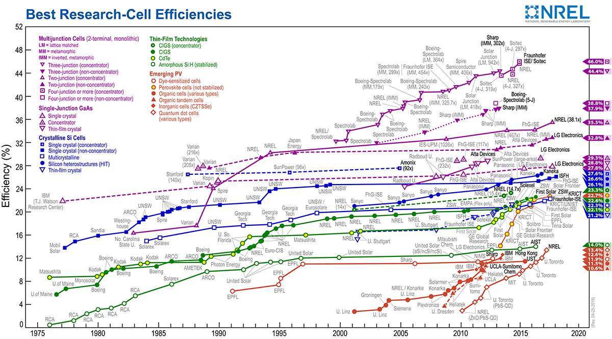