Abstract
Displays represent information visually, so they have become the fundamental building block to visualize the data of current electronics including smartphones. Recently, electronics have been advanced toward flexible and wearable electronics that can be bent, folded, or stretched while maintaining their performance under various deformations. Here, recent advances in research to demonstrate flexible and wearable displays are reviewed. We introduce these results by dividing them into several categories according to the components of the display: active-matrix backplane, touch screen panel, light sources, integrated circuit for fingerprint touch screen panel, and characterization tests; and we also present mechanical tests in nano-meter scale and visual ergonomics research.
Introduction
The demand for user-friendly electronics has rapidly increased people want devices that perform well and are convenient to use. Therefore, many research groups have studied flexible or wearable electronics to demonstrate user-friendly electronics that can be conformally mounted on various objects with non-planar surfaces.1, 2 Among these studies, displays are the most typical visualization devices, and flexible or wearable displays have also been studied to improve convenience-of-use, such as weight reduction, improved portability, and robustness.3, 4 Because wearable displays have to tolerate the deformation degree of human skin (with a tensile strain of approximately 20–30%),5, 6 these wearable displays and the electronics associated with them must be able to stretch.
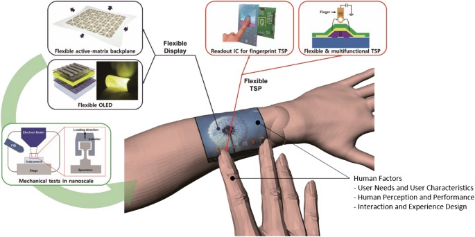
Figure 1 shows the research direction of Ulsan National Institute of Science and Technology (UNIST) flexible display research center. A flexible panel is composed of a flexible backplane, a flexible display, and a flexible touch screen panel (TSP). The flexible backplane is made up of flexible material: a group of parallel electrical connectors acts as the structural skeleton of the flexible panel. A flexible display or a flexible TSP are added on the flexible backplane. Because these additions are stretchable and flexible, it is possible to make various shapes of flexible devices, such as a curved display or portable electrical paper. After the flexible panel is fabricated, it must then be tested for performance. In UNIST research center, nano-scale mechanical tests are also performed to evaluate the panel’s flexibility. A driving integrated circuit (IC) or a readout IC support the flexible panel environment. When a flexible panel is stretched or bended, different characteristics of the panel may change, and the IC can maintain constant operation and performance. In addition, ergonomics research is required to consider the factors impacting the human user, such as user physiology and human perception.
This paper reviews the research of UNIST display center. In the section ‘‘Research at UNIST Display Center’’, research that is underway is presented. In the first three subsections, a flexible panel is described, including a flexible active-matrix backplane, a flexible multi-functional transparent touch screen panel, and flexible electronics and materials. In fourth subsection, the methods by which the mechanical properties of constituent materials in flexible display devices are characterized are presented, and in fifth subsection, a readout IC for the flexible TSP is presented. Lastly, in last subsection, the visual ergonomics research on new types of displays is presented. The last section presents the conclusions.
Research at UNIST display center
Flexible active-matrix backplane for flexible display
Backplanes are the most essential component of electronics because they can connect in parallel with each other and control the electrical signals of devices. As opposed to the passive-matrix form, the active-matrix backplane allows selective access to each component with a rapid response while maintaining a high-circuit density by sharing electrode lines. Despite many advantages of active-matrix backplanes, the realization of deformable active-matrix backplanes with reliable operation is very challenging. This is because three electrodes (gate, source, drain) of each component are connected to different word and bit lines and grounds, and the failure of only one single component can lead to the failure of the whole backplane. Therefore, it is important to minimize stress during deformations of thin-film transistor (TFT)-based electronics. The deformability of backplanes is commonly obtained by modifying device materials and structures to accommodate most of the strains induced by bending, folding, and even stretching. These modifications can be classified into two approaches: one uses intrinsically flexible materials (e.g., ultrathin or elastomeric materials) and the other uses an engineered substrate.
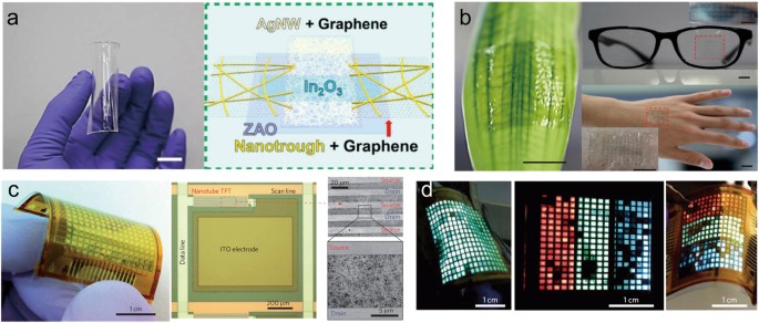
The most basic method of obtaining flexibility or bendability is the adoption of ultrathin materials as the TFT backplane components.7 This is because all materials exhibit increased flexibility when their thickness decreases. At UNIST, Park’s research group has fabricated a stretchable and transparent backplane based on oxide semiconductor TFTs with graphene-Au nanotrough (AuNT) hybrid structured interconnect electrodes.8 The resulting electrodes exhibited low sheet resistance of 1 ± 0.1 Ω/sq at 91% transmittance, and can be stretched up to the strain of 50% with the 60% increase in resistance. The skin-attachable, highly flexible, and transparent oxide semiconductor TFT arrays on a 2-µm-thick polyimide (PI) substrate were demonstrated by using graphene-AuNT hybrid source/drain and gate electrodes, as shown in Fig. 2a, b. In addition, no fracture was found on the oxide semiconductor TFT regions due to the thin thickness of the backplane (~2 µm) and the improved flexibility of the TFT regions. Javey and coworkers have demonstrated a flexible display that is composed of a flexible carbon nanotube (CNT)-based backplane and flexible organic light-emitting diode (OLED) pixels as depicted in Fig. 2c, d (ref. 3). The flexible display was fabricated on a 24-µm-thick PI film, and the total thickness of the devices (excluding the substrate) was <2 µm. Therefore, the flexible backplane showed stable electrical characteristics even during the bending states (where the bending radius was 4.2 mm), and the OLED pixels also performed with negligible degradation from the deformations (where the bending radius was 4.7 mm). Consequently, this fabricated display also demonstrated flexibility because of the deformability of the devices.
Flexible backplane for display fabricated by a thin-film process. a Photo (left) of the TFT array sample made by graphene–AuNT hybrid electrodes on a transparent polyimide substrate. Scale bar: 1 cm. A schematic diagram (right) of the TFT layout. b Photos of the TFT arrays transferred onto: a leaf, eyeglasses, and the skin of human hand. All scale bars: 1 cm. a–b Reproduced with permission from ref. 8. Copyright 2014, American Chemical Society. c Photo (left), optical micrograph (middle), and scanning electron micrographs (right) of flexible backplane. d Photos of operating flexible display combined with backplane and OLED pixels. c–d Reproduced with permission from ref. 3. Copyright 2013, Nature Publishing Group
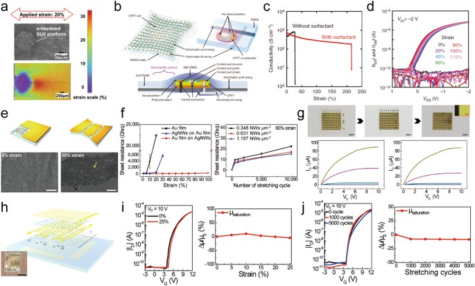
Many studies have demonstrated flexible electronics with various methodologies. However, in the case of the aforementioned methods, mechanical stresses continue to be induced on the brittle electronic materials, even though the stresses are relieved. Therefore, the mechanical stresses generate fatigue on the electronics during repetitive or constant deformations, and the accumulated fatigue causes severe problems that deteriorate the performance and reliability of flexible TFT backplanes. Consequently, reducing fatigue becomes a key challenge to realizing highly flexible and stable backplanes or electronics. The typical method of reducing mechanical fatigue on the TFT backplane is the adoption of device islands-interconnect designs. These designs are based on engineered substrates that are composed of materials with different values of elastic modulus.9,10,11 These “engineered substrates” can be designed to manipulate the distribution of mechanical strain by patterning the rigid regions to take advantage of the huge difference in elastic modulus, as shown in Fig. 3a.9 Hence, most of the mechanical deformations on engineered substrate systems occur on the soft regions, and there is little strain on the rigid components. The electronic materials on the rigid components can thereby be protected from mechanical failure. However, these engineered substrate systems are only as reliable as the flexible electronics used on the stretchable interconnects, where the large strain occurs. Consequently, the stretchable interconnects should have both low resistivity and high stretchability to prevent the degradation of the performance of the backplane or electronics. Table 1 summarizes the recent advances in stretchable interconnect technology.12,13,14,15,16 In order to realize highly flexible or stretchable backplanes based on the engineered substrate systems, further study on stretchable interconnects should be conducted. Another advantage of engineered substrates is the exclusion of a transfer process. Someya and coworkers have presented stretchable organic thin-film transistor (OTFT) backplanes on the engineered substrates.12, 17 The OTFT backplanes exploited the engineered substrates and stretchable interconnects, which consisted of silver flakes embedded in elastomer (Fig. 3b). The stretchable conductors showed high stretchability at over 200% strain as plotted in Fig. 3c. Based on these systems, the stretchable backplane also demonstrated superb stretchability up to the strain of 110% (Fig. 3d). In addition, Kim et al. have also demonstrated a reversibly foldable TFT backplane based on the oxide semiconductor (indium oxide (In2O3)), which shows high performance and is used in the conventional backplane.13 To achieve stable operation during the folded states, they designed stretchable conductors that are composed of Au film on an elastomer embedded with silver nanowires (AgNWs), which can be exploited as interconnects (Fig. 3e). The designed stretchable conductors exhibited stretchability up to the strain of 100% and also exhibited stability against cyclic tests (10,000 times with the 80% strain), as shown in Fig. 3f. Because of these superior interconnects and engineered substrates, the oxide semiconductor TFT backplane also showed high stability during the folding states without any degradation (Fig. 3g). In addition, Park and his team have also studied stretchable TFT backplanes based on these two systems Fig. 3h. Their TFT backplanes also provided reproducible performances up to the strain of 25%, as shown in Fig. 3i, and showed high stability against fatigue (5000 times with the 20% strain), as shown in Fig. 3j. The reliability of the stretchable TFT backplane is affected by the strain isolation effect of engineered substrates and the high stability of stretchable interconnects (Au film on AgNWs-embedded elastomer).
Device islands-interconnect design for highly flexible TFT backplane. a Simulation of strain manipulation at the top surface of the engineered substrate. Reproduced with permission from ref. 9. Copyright 2013, American Institute of Physics. b Schematic illustrations of OTFT backplane on engineered substrate. c Conductivity dependence on tensile strain in printed elastic conductors with and without surfactant. d Transfer characteristics of OTFT according to the tensile strain. b–d Reproduced with permission from ref. 12. Copyright 2015, Nature Publishing Group. e Schematic images (top) and scanning electron micrographs (bottom) of stretchable conductor (Au film on AgNWs-embedded elastomer) before and after stretching. Scale bars: 5 μm. f Resistance dependence on tensile strain (left) and cyclic numbers (right) of the stretchable conductor (Au film on AgNWs-embedded elastomer). g Images (top) and output characteristics (bottom) of foldable TFT backplane on engineered substrate before and after folding. Scale bars: 5 mm (black) and 100 μm (red). e–g Reproduced with permission from ref. 13. Copyright 2016, Royal Society of Chemistry. h Illustration and photograph (inset) of stretchable TFT backplane on engineered substrate. i Electrical properties of device in h according to the mechanical strain (up to a strain of 25%). j Electrical properties of device in h according to the number of cycles
Flexible multi-functional transparent TSP
TSP has become a key element in various electronic devices such as televisions (TVs), hand-held devices, and laptop computers, and the increasing demand for a more interactive user interface has influenced the broadening of the TSP application area.18,19,20 There are two different types of TSP. One is the resistive type, which senses the resistance change caused by the deformation of the TSP film.21 The other is the capacitive type, which senses the capacitance change associated with the disturbance of fringe electric fields due to the finger touch.22 The capacitive TSP has some benefits over its resistive counterpart in terms of high resolution, multi-touch capability, and durability, although its fabrication processes are more costly and the scaling to a large size is more challenging. The capacitive TSP has another advantage in the sense that its functionality can be easily extended to detect several different signals simultaneously by adopting flexible and stretchable materials and designing proper device structures. The recent rapidly growing demand for the human-machine interface devices that are used in robotics,23 internet of things,24 and personal health-care monitoring systems25 requires the enhanced functionalities of the associated sensors to have a machine acquire several sensing capabilities in the manner of a human. The capacitive TSP is considered to be a quite suitable device for human-machine interface applications due to its multi-sensing capabilities.
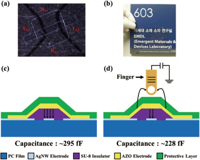
The research activities for developing TSP technologies at UNIST have been devoted mainly to exploring new materials, device structures, and device fabrication processes for multi-functional flexible and stretchable TSPs. One noticeable achievement is the development of the highly flexible capacitive TSP with AgNW diamond-pattern electrodes and transparent bridge structures formed on a polycarbonate film.26 Figure 4 shows the structure and touch-sensing capability of the fabricated TSP. As shown in the Fig. 4, the bridge structure is composed of an epoxy polymer (SU-8)-based bridge insulator and an Al-doped zinc oxide (AZO) bridge electrode. In order to secure the stable and robust connection between the AZO bridge electrode and the AgNW diamond-pattern electrodes over the bridge insulator, the side-wall slope of the bridge insulator is made as low as possible with our unique photolithography process, in which the exposure time is extended beyond the optimized value for forming vertical side-walls. With the extended exposure time, the lower part of the SU-8 layer immediately adjacent to the direct exposure region can be sufficiently exposed to the stray ultraviolet (UV) light scattered from the substrate, leading to the formation of a bridge insulator with a low side-wall slope. The fabricated TSP sample was found to be highly flexible and transparent and also showed good touch-sensing performance. The measured capacitance changes by ~22.7% with the finger touch.
a Dark-field optical microscope image of fabricated TSP sample showing the AgNW diamond-pattern electrodes (Rx, Tx), SU-8 bridge insulator, and AZO bridge electrode. b Photo demonstrating the transparency of the fabricated TSP sample and a schematic of the working principle of the fabricated TSP: electric field line configurations and measured capacitances c before and d during touching. a–d Reproduced with permission from ref. 26. Copyright 2015, Optical Society of Korea
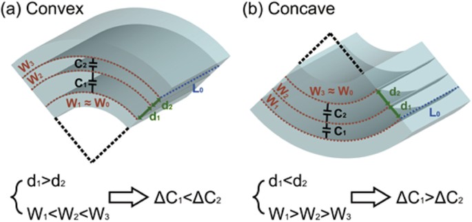
Another relevant achievement is the invention and experimental demonstration of a stretchable dual-capacitor multi-sensor capable of simultaneously sensing touch, curvature, pressure, and strain. There have been great advances in the field of multi-functional capacitive sensors over the past years. However, the multi-functional capacitive sensors developed so far are equipped with only a single capacitor, and thus they cannot recognize the direction of an external stimulus applied onto the sensor. In addition, several different sensing modes implemented on these sensors have not been clearly classified.27,28,29 In contrast, our dual-capacitor sensor is constructed with two capacitors stacked vertically. As opposed to the single-capacitor sensor, the dual-capacitor sensor can detect the type, direction, and strength of an external stimulus by relying on the relative capacitance changes of the two stacked capacitors. In order to evaluate its scale-up potential, a 5 × 5 array type of stretchable dual-capacitor sensor, based on AgNW crossing electrodes and polydimethylsiloxane (PDMS) insulators, has been fabricated. As an example demonstrating the capability of the dual-capacitor sensor for detecting both the direction and the strength of an external stimulus, Fig. 5 shows the working principle of curvature sensing. When the dual-capacitor is curved in the convex shape as shown in Fig. 5a, the top electrode (W 3) will be stretched more than the middle electrode (W 2). Meanwhile, the bottom electrode will stretch very little (W 1 ≈ W 0, where W 0 represents the width of the AgNW electrode when the sensor is relaxed). Also, the upper PDMS insulator sandwiched between the top and middle electrodes will become thinner than the lower one sandwiched between the middle and bottom electrodes. Hence, the capacitance of the upper capacitor (C 2) will increase more than that of the lower capacitor (C 1). If the dual-capacitor is curved in the concave shape, the same form of relations will be obtained with the parameters of the upper and lower capacitors exchanged, as shown in Fig. 5b. As with the sensing of curvature, the direction and strength of pressure, strain, and touch can also be detected clearly from the signs and relative magnitudes of the capacitance changes of the upper and lower capacitors. In addition, we developed a logical flow for unambiguously classifying the physical stimulus given to the dual-capacitor sensor unambiguously as one of curvature, pressure, strain, and touch by analysis of the measured capacitances of the two capacitors. This classification flow can be readily adopted in the driving circuit of this sensor.
Based on their superb operational performances and functionalities, the flexible and stretchable TSP devices developed at UNIST, including the two introduced above, are expected to significantly enrich the information communicated between humans and machines. Thus, it is quite probable that these devices will be used extensively in various future information technology applications.
Flexible electronics and materials
Flexible light sources are important parts in flexible display applications because they determine long-term stability and commercial value of practical flexible displays under continuous mechanical stress. Thus, flexible light sources should have sufficient light-emission efficiency and mechanical stability. Generally, OLEDs have been mostly spotlighted candidates for flexible light sources because OLEDs consisted of organic materials and they have outstanding mechanical flexibility compared with inorganic LEDs.30,31,32 Moreover, they can be fabricated by cost effective solution process such as roll-to-roll process, spin-coating and spray-coating.33
Following constituent materials of flexible OLEDs, there are four major research issues (substrates, electrodes, light-emissive materials, and encapsulation) to be perfectly developed for practical future applications; flexible substrates, electrodes, light-emissive materials, and encapsulation. Here, we briefly introduce technical research issues with four sections and suggest future research directions of flexible OLEDs.
Almost all of the macroscopic flexibility of flexible OLEDs comes from substrates. The important properties of flexible substrates are mechanical flexibility, thermal stability, optical transparency, and gas barrier properties.34,35,36 Generally, typical materials for flexible substrates are polymer-based solid materials such as polyethylene terephthalate,34 polyethylene naphthalate,35 and PI.36 Exceptionally, thin glass (thickness = ~100 μm) has been used for flexible substrates,37 however such thin glass (to the best of our knowledge) is still brittle under some forms of mechanical deformation. To date, primarily polymer substrates have been evaluated as appropriate materials for flexible substrates.
In general, indium tin oxide (ITO) has been used as conventional transparent conducting electrodes for organic optoelectronic devices in practical and research areas including OLEDs because it has good optical and electrical properties with high transmittance.38 However, ITO is not suitable for flexible OLEDs because of its brittleness and high cost.39 Transparent and flexible electrodes are very important in flexible OLEDs because they affect charge carrier injection and light extraction by low sheet resistance and high optical transmittance, and thus finally device efficiency. Consequently, many researchers have developed flexible and transparent electrodes to replace ITO and the candidates have been demonstrated as below.
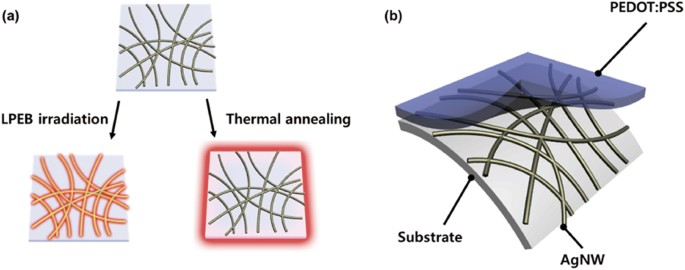
Highly conductive poly(3,4-ethylenedioxythiophene):poly(styrenesulfonate) (PEDOT:PSS) have been investigated for flexible electrodes with highly smooth surface, optical transparency, easy processes, and enhanced electrical conductivity up to 4380 S/cm by doping with polar solvents or concentrated sulfuric acid.40 Metal nano-materials such as AgNWs,41 nano-meshes,42 and copper nanowires (CuNWs)43 have been studied for highly conductive and flexible electrode. AgNWs and CuNWs are fabricated as a dispersion by solution-based chemistry, and easily coated on substrates by low-cost solution processes such as spin- or spray-coating. However, they have non-uniform surface coverage and unlike two-dimensional (2D) materials like graphene, since they are networks of ‘‘1D’’ structures they cannot cover all the surface (that is, obviously there are gaps), which might impact certain configurations. In addition, high junction–junction contact resistance in percolation networks results in low(er) electrical conductivity even though the conductivity of the individual metal nanowires is (relatively) high. This causes large leakage currents and non-uniform light emission that mean low efficiency OLEDs. Many researchers have suggested various welding processes such as thermal welding,41 plasmonic welding,44 and large pulsed electron beam (LPEB)45 welding to improve the electrical and mechanical properties of such networks. AgNWs with LPEB welding was said to yield mechanically robust percolation networks with low electrical loss for stable flexible OLEDs under continuous and large bending stress, as shown in Fig. 6. In addition, hybrid flexible electrodes composed of PEDOT:PSS and AgNWs were said to be mechanically durable and robust OLED characteristics were said to be obtained.46 Carbon materials such as graphene47 and CNTs48 are also under active study in flexible electrode applications.
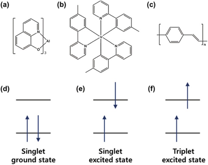
Organic semiconductor materials for OLEDs are classified as two types depending on the mechanism of light emission. Firstly, fluorescent emissive materials such as electroluminescent polymers emit light by relaxation of singlet excitons under an external electric field. Typical electroluminescent polymers used in polymeric LEDs (PLEDs) include poly(p-phenylene vinylene) (PPV)49 and polyfluorene.50 They are fabricated by solution processes such as spin-coating, bar-coating, spray-coating, and inkjet-printing. The electroluminescent polymers can be readily modified by control of chemical and morphological properties and desired mechanical properties for flexible OLEDs can be obtained with control of the polymer chain. The emitter type are phosphorescent materials that emit light by triplet exciton relaxation. In general, they consist of organometallic dyes and polymer host materials such as poly(9-vinylcarbazole). They phosphoresce with highly efficient quantum yield approaching 100%, compared with 25% for fluorescence emission.51 Organometallic dyes can be chosen to achieve target wavelength and color,52 as shown in Fig. 7.
Most components of flexible OLEDs are organic materials that can easily react with oxygen and moisture because plastic substrates and other components have low gas barriers. The water vapor transmission rate (WVTR) is strongly related to the long-term stability and feasibility of practical flexible OLEDs. OLEDs generally require a WVTR of approximately 10−6 g/m2∙per day, which is a very low value compared to inorganic LEDs.53 A glass “lid” and moisture absorbable getter with a UV-curable epoxy resin in an inert chamber is generally used to encapsulate OLEDs. However, this process cannot be applied to flexible OLEDs because the glass lids used to date are too rigid. Therefore, thin-film encapsulation (TFE) with soft materials has been investigated for flexible encapsulation but the TFE techniques result in an low barrier to permeation, compared with other rigid encapsulations with higher-density barrier films. Some researchers have suggested stacked multi-layered TFE with heterogeneous thin films54, 55 and special patterning techniques to increase the penetration path length of gas molecules.56 Stacks of polymers and metal oxide nano-materials or carbon materials have thus been studied for flexible TFEs. For instance, layer-by-layer coating method with montmorillonites; metal-oxide nano-sheets, and poly(viny alcohol) (PVA) and poly(ethyleneimine) on 100 μm of poly(ethersulfone) substrates, have been reported to result in a WVTR of 5.6 × 10⁻³ g/m2∙day, as shown in Fig. 8.57
For next-generation displays, flexible and light-weight OLEDs are an appropriate candidate because of their excellent light emission, and mechanical flexibility. Currently available components of flexible OLEDs including substrates, electrodes, emissive materials and encapsulation layers, are still insufficient to achieve practical flexible OLEDs with stable performance under mechanical deformation. Consequently, achieving reliable components of flexible OLEDs such as (1) flexible substrates and encapsulation layers with good barrier properties, (2) transparent electrodes that are mechanically robust under deformation and have low sheet resistance, and (3) flexible materials that emit light efficiently, remains to be solved for commercial applications.
Characterization of mechanical properties of the materials in flexible display devices
Recently, flexible display devices have attracted widespread attention as an alternative to rigid devices because of their portability and comfort for long time wearing. For the relevant applications, when the devices undergo mechanical deformations such as bending and stretching, the thicknesses of the constituent materials usually decreases and all layers suffer a tensile stress at the outside of each layer.58 Because fracture(s) in these devices initiate at the weakest part(s) of the material(s), the intrinsic mechanical properties of each layer impact the device’s reliability and durability. However, because of their small scale and typically ‘‘ultra-thin’’ thickness, sample preparation and handling pose significant challenges to mechanical testing.
Most researchers reference the mechanical properties presented in previous studies based on theoretical calculations or experimental results measured on much larger length scales than the actual scale(s) used in devices. However, current computational methods have inherent limitations and often deviate from the experimental results, and these cannot be considered truly representative because of the potential effect of the device’s size on its properties. Sharpe et al.59 proposed two considerations that should be applied to specimens in small-scale testing: they should have a scale similar to the actual structural components, and they should be manufactured following the same processes as the actual components. To evaluate the structural integrity of small-scale flexible devices under mechanical load, several mechanical tests are performed; the mechanics of each is briefly described below, and then we present the use of such tests in probing the mechanics of relevant components of flexible electronics.
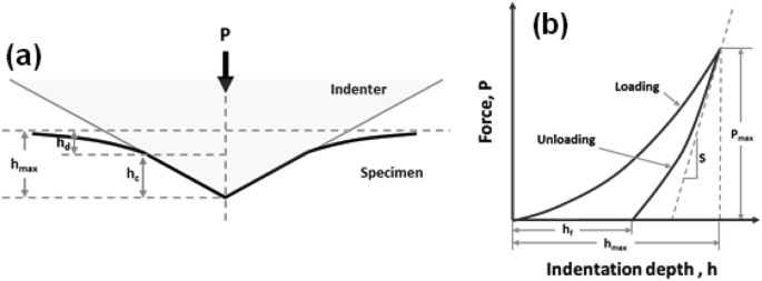
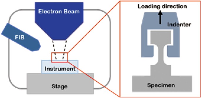
Nanoindentation was developed to measure the mechanical properties of small-volume and thin-film materials. The outstanding merit of nanoindentation is that it has a simpler procedure for small-scale sample preparation compared with other mechanical tests. During indentation with a sharp-tipped indenter on the sample surface, as shown in Fig. 9, the force and indentation depth are continuously measured over an indentation depth ranging from a few tens of nanometers to a few micrometers. The hardness and elastic modulus can be calculated from the force-indentation depth data using the Oliver-Pharr method59,60,61:
The hardness H is given by the Eq. 1, which relates the force to the indentation depth, where P is the applied force and A c is the projected contact area. The reduced modulus is given by
where the slope of the curve upon unloading, dP/dh, is indicative of the stiffness S of the contact. From the reduced modulus, the elastic modulus of the sample E can be calculated as
where E and ν are the elastic modulus and Poisson’s ratio for the sample, respectively, and E i and ν i are the same for the indenter which is usually made of diamond. To calculate the projected contact area A c as a function of the contact depth, h c, it can be calculated by subtracting the elastic deflection, h d, on the sample’s surface from the maximum indentation depth h max:
where θ and ε are the equivalent angle of the indenter and a constant that depends on the indenter geometry, respectively.
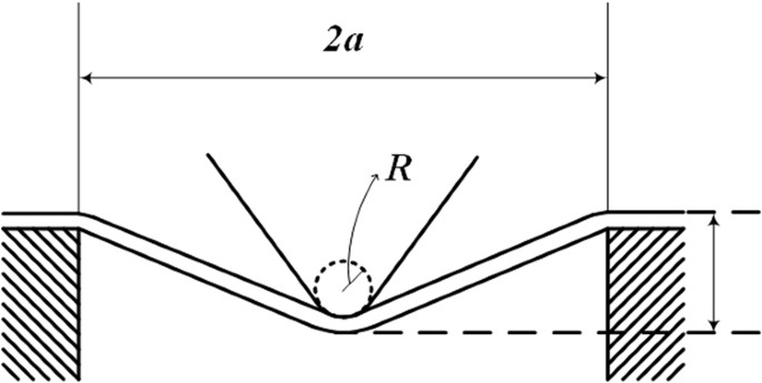
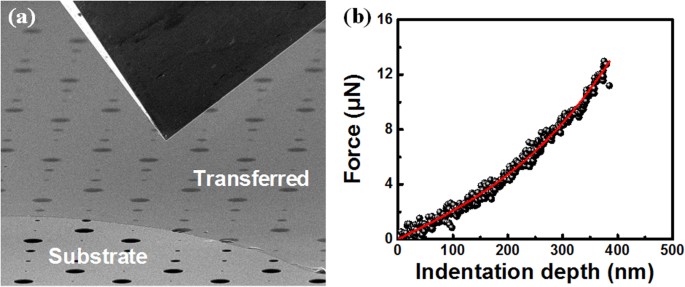
As mentioned above, nanoindentation can measure small-scale materials such as thin-films, nano-particles, etc. However, when the sample thickness is below approximately 100 nm, it is difficult to use nanoindentation because of the “1/10 rule”, which states that the maximum indentation depth is approximately 1/10 of the sample thickness, to exclude the substrate adversely influencing the experimental results. Lee et al.62 applied hole-nanoindentation on monolayer graphene transferred onto a hole-patterned wafer using indentation with atomic force microscopy as shown in Fig. 10. The mechanical properties of this film were calculated from force-penetration depth data based on the following non-linear elastic response model:
where F and δ are the applied force and deflection at the center, respectively; \(\sigma _0^{2D}\) and E 2D are the pretension and elastic stiffness, respectively; and q and a are functions of Poisson’s ratio and the radius of the patterned hole, respectively. The maximum stress under indentation, \(\sigma _m^{2D}\), has been defined by a simple equation as a function of the applied force:
Flexible display devices contain many laminated structures composed of sub-micrometer-scale thin films. At UNIST, we evaluated the mechanical properties of one of these components using modified hole-nanoindentation. PDY-132 (Merck, Germany, commercially sold as “Super Yellow”) is a ‘‘high-performance polymer’’ that emits yellow light. In our evaluation, PDY-132 was spin-coated on a clean glass substrate. The sacrificial layer was selectively dissolved to fabricate free-standing films with the same dimensions as the actual devices. We fabricated hole-patterned Si wafers using the deep reactive ion etching method. The patterned hole size was proportional to each film thickness, so that the diameter of a hole was less than 1% of the film thickness.63 A flake of Super Yellow from our sample preparation was transferred onto the hole-patterned substrate, and we then used a commercial in-situ nanoindenter (PI-87, Hysitron, USA), which can measure force and displacement with resolutions of <3 nN and <0.02 nm, respectively. This equipment enables nanoindentation testing in a scanning electron microscope (SEM) chamber, so that deflection by the indenter on the center of the hole can be directly observed in real time, as in Fig. 11. The elastic modulus of the hole-indentation was found to be 4.89 GPa, and its fracture strength was 1.19 GPa.
Uchic et al.64 reported a new technique for measuring the mechanical properties of nano-scale materials. They fabricated a micrometer-scale cylindrical sample using a focused ion beam and performed uni-axial compression tests with a flat punch indenter, referring to this method as “pillar compression”.65,66,67 At UNIST, this approach was extended to perform uni-axial tensile tests by equipping the nanoindenter in the SEM with custom-fabricated tension grips, as shown in Fig. 12. Tensile testing is the most fundamental method of evaluating a material’s inherent mechanical properties, such as yield strength, strain-hardening exponent, ultimate tensile strength, etc. As mentioned above, in-situ testing enables precise observations of sample deformations in real time, with simultaneous imaging during testing. Various indenters are also expected to enable stretching and bending tests of constituent materials in flexible display devices.
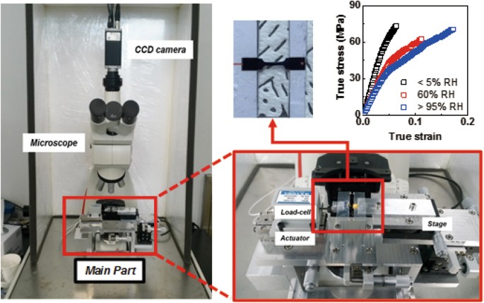
Flexible display devices contain many organic materials, such as polymer films, active materials, and electrodes. However, mechanical tests of organic materials in high vacuum conditions in SEM and transmission electron microscopy are limiting in that organic materials are (in real environments) highly affected by surrounding environmental conditions such as humidity and temperature; it is important to measure mechanical properties in actual operating environments. A nano-UTM can be used to control environmental conditions using a controlled humidity chamber and heating block because the machine is based on an optical microscope, as shown in Fig. 13. Images of gauge sections during tensile tests are observed by a charge-coupled device camera in real time, and strain is analyzed from the images based on digital image correlation. Constituent materials in flexible display devices are macroscopically visible and their thicknesses are generally in the nanometer-scale range. PEDOT:PSS is widely used for organic transparent conducting electrodes, and PEDOT:PSS thin films are fabricated by natural drying after drop casting on a substrate. A tensile sample was fabricated by a mechanical press, and the gauge length and gauge width were 4 and 1 mm, respectively, as in the standard ASTM E8 test. We performed tensile tests of PEDOT:PSS in three different humidity conditions by nano-UTM, and the results are summarized in Fig. 13. The yield strengths of the samples tested in the lowest humidity environment were greater than those of other samples, and the fracture strain decreased as humidity increased.
Readout IC for the fingerprint TSP on the flexible display
In recent years, fingerprint mutual capacitive TSPs with flexible displays fabricated from flexible plastic materials have attracted much attention because of the development of transparent fingerprint sensors embedded in flexible displays that are also thin and impact-resistant. As security protections for electronic devices such as smart phones become increasingly important, a fingerprint sensor has been integrated on the device’s home button because the fingerprint sensor is not transparent. However, a mutual capacitive transparent fingerprint TSP must be developed on the display itself because a wearable device does not have a home button, and the screen sizes of smart devices must otherwise be enlarged.
In the fingerprint TSP, capacitance sensitivity is very important to capture the fingerprint image. The distance difference from a fingerprint’s valley to its ridge and to the sensing electrode of the fingerprint TSP is approximately one or two hundred μm.68, 69 Current device protection layers have become thicker to protect components, and therefore the capacitance sensitivity of the fingerprint TSP is much smaller because of the thick glass cover, which deteriorates the fingerprint image. For a fingerprint TSP on a flexible display, the capacitance sensitivity of the fingerprint TSP can be effectively enhanced because of the thinness of the flexible display compared to previous rigid displays that incorporated fingerprint TSPs.
To make a flexible TSP, a flexible and transparent material must be used for the TSP electrode. However, variation in load becomes a concern when the flexible electrodes of the fingerprint TSP are bent or stretched, which can interfere with capturing the fingerprint image. Because the capacitance difference of the mutual capacitive fingerprint TSP from the ridge to the valley is several hundred atto-farads, the effect of the load variation due to a bent or stretched TSP will be very critical.
Both the flexible fingerprint TSP and post-processing are required to capture the fingerprint image in the fingerprint TSP on the flexible display. A readout IC for the flexible fingerprint TSP is required to distinguish the atto-farad capacitance difference in the fingerprint TSP noise environment on the flexible display. Post-processing is also necessary to compensate for the load variation due to the bent or stretched display.
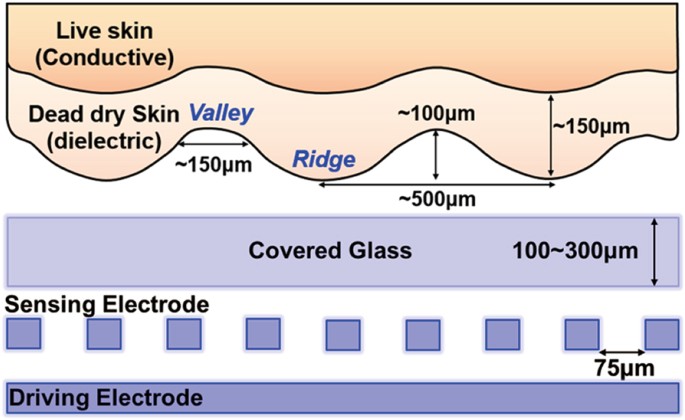
Figure 14 shows a simplified structural model of the human skin and a fingerprint TSP. The human skin is composed of the dermis layer and the epidermis layer, which includes the valleys and ridges of the fingerprint. The epidermis layer consists of dry dead skin cells, which have low electrical conductivity; this region behaves as a dielectric. The dermis layer consists of live cells, which are moist and electrically conductive. The mutual capacitive touch screen sensor measures the difference in permittivity between the ridge surface skin and the air in the valleys. A fingerprint consists of many ridges and valleys on the surface of the finger. The width of the ridges varies in the range of approximately 0.5–0.7 μm, and the widths of the valleys are approximately 0.15 μm. The depth of the valley varies in the vicinity of 150 μm. If the depth of the valley is lower than 150 μm, the capacitor difference due to the valley and ridge is also very small.68, 69
When the thickness of the covered glass of the flexible display is almost 0.2–0.3 mm, the mutual capacitance difference from the valley to the ridge is almost 50–150 atto-farad. As the thickness of the display panel increases, the mutual capacitance difference is reduced. The thickness of the rigid glass is larger than that of the flexible display panel, which induces a capacitance difference between the valley and the ridge of only several atto-farad.
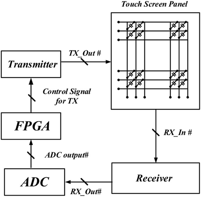
Figure 15 shows the overall block diagram of a touch screen readout IC.70 The system is composed of a transmitter, analog-front-end, analog-to-digital converter (ADC), and field programmable gate array (FPGA). A transmitter sends a driving signal to the electrode of the lower layer in the TSP. This driving signal is converted to the current signal, which is proportional to the mutual capacitor value. These current signals go through the analog-front-end circuit, which converts the current signal to a voltage signal depending on the driving signal and mutual capacitor values. The outputs of the analog-front-end are connected to the ADC, which converts the analog signal to the digital signal. In the FPGA, the processor acquires raw data from the node of the fingerprint TSP depending on the output of the ADC. These raw data are converted to the fingerprint image.71
A proposed high voltage transmitter and the low-noise, low-capacitance sensing circuits for the fingerprint touch screen panel. Reproduced with permission from ref. 70. Copyright 2014, IEEE
When the fingerprint TSP is bent or stretched, the mutual capacitance and resistance change.69, 72 Because the load variations occur, an offset due to the bending and stretching also occurs. To solve the load variation issue, the analog-front-end circuit should detect bending or stretching states. An offset calibration is then required, and is implemented by acquiring and subtracting offset data from the raw data.
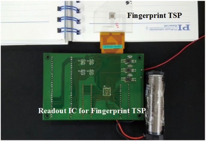
Figure 16 shows the fingerprint TSP and the test board designed for fingerprint recognition, which includes a 42 × 42 fingerprint TSP with a resolution of 280 dpi, as well as a receiver, transmitter, external ADC, and back-side FPGA. The transmitter has 42 channels and is designed for a high-voltage driving signal. The receiver also has 42 channels and is designed to sense low-noise and low-capacitance differences and offers a fast response to acquire the offset data and the raw data. During post-processing, the offset from the bending and stretching is canceled by subtracting the offset data from the raw data.
A low-noise, low-offset, and fast-response receiver is required to acquire a fingerprint image in the mutual capacitive fingerprint TSP on the flexible display. In addition, the post-processing is also required to compensate for the load variation issues that occur because of the flexible TSP’s unique characteristics. A readout IC with high accuracy and a fast response and an effective algorithm for cancelling the offset due to the load variation are both required to achieve an effective fingerprint TSP on the flexible display.
Visual ergonomics research on new types of display
Display products are frequently used for the purposes of task efficiency or leisure. Because long-term and/or frequent use of visual display terminals (VDT) is harmful to our health, ergonomic interventions including ergonomic displays are essential. Users of VDTs suffer from headaches, nausea, visual fatigue, and/or musculoskeletal disorders, which are comprehensively called VDT syndrome or computer vision syndrome. Recently, curved displays have been adopted as a new form of display for several types of commercialized visual display products (smartphones, smart watches, smart bands, TV, and computer monitors). Visual display products that adopt bendable, foldable, or rollable displays are expected in the near future. Existing guidelines for performing visual tasks on flat or convex displays (e.g., ISO 9241) require that characteristics of new displays be evaluated from the perspective of the health of the human user. New types of display are different from conventional displays in terms of optical characteristics, and ergonomic investigations should thus be more focused on visual perception, comfort, and fatigue, among other factors in the ergonomics field.
Visual ergonomics is one prominent research area in terms of ergonomics related to display and visual perception. Visual ergonomics is defined as the multidisciplinary science concerned with understanding human visual processes and the interactions between humans and other elements of a system. Visual ergonomics applies theories, knowledge and methods to the design and assessment of systems, optimizing human well-being and overall system performance. Relevant topics include, among others: the visual environment, such as lighting; visually demanding work and other tasks; visual function and performance; visual comfort and safety; optical corrections and other assistive tools.
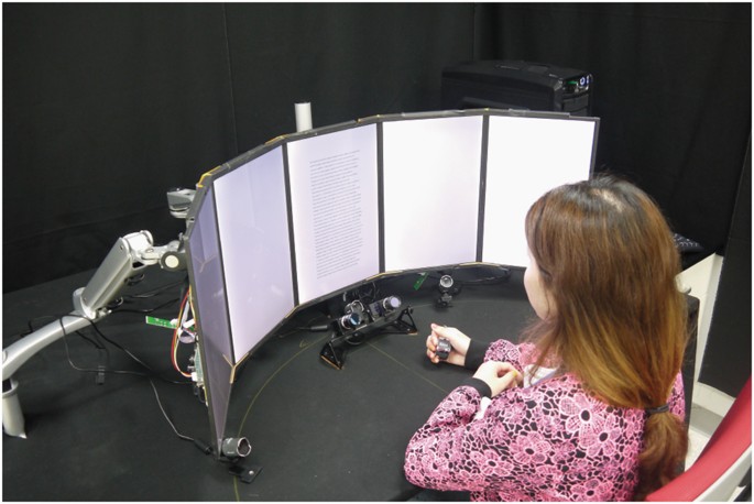
New forms of display are characterized by optically different properties, which consequently affect visual perception (Fig. 17). Curved displays have been reported to have advantages73 and disadvantages, such as image distortion due to excessive display curvature, while accounts on the corresponding features of other new displays (such as bendable, foldable, and rollable) are somewhat limited. Bendable displays can be used to provide new interaction methods (e.g., bending to zoom), and foldable or rollable displays can provide both large screens and portability. In order to commercialize foldable displays, the folded area should be sufficiently durable in both of two aspects: dynamic durability with regard to frequent folding and unfolding, and static durability with regard to folding or unfolding after longer periods of non-use. On the other hand, the folded screen area can also distort images. As for rollable displays, it is important to be able to easily extract and retract the rollable screen.
When determining ergonomic display curvatures, several factors should be considered, including the viewer, media content, task, and environment. Regarding the viewer, general characteristics of visual perception as well as age-related factors should be considered. It is also important to consider the effects of media content (static, dynamic, 2D, or three-dimensional) on the viewer’s perception and ocular health. Task duration and the work-rest schedule are also important to promote ergonomic conditions during VDT tasks. Finally, the viewing environment is important in terms of its illumination, light reflection, humidity, viewing distance, viewing angle, and lateral viewing position.
When evaluating visual displays, the following measures can be used. Many diverse subjective rating scales are available to assess perceived visual comfort or discomfort, visual fatigue, and cyber-sickness (e.g., ECQ, SSQ). In addition, the concept of presence, or immersive feeling, has become more important as an essential element of a satisfactory viewing experience through any media. Objective measures related to the viewing experience include critical fusion frequency to assess mental stress and visual fatigue, change in pupil size, and eye blink frequency and duration.
It is also important to understand how our visual perception operates to better inform our visual display designs. Related concepts include the just noticeable difference (JND), horopter, and depth perception. For example, JND values for display curvature can be used to determine a specific display curvature within the JND range, within which our perception is regarded equal. The horopter concept contributes significantly to the advantages offered by curved displays in comparison with flat displays. Horopter is “the locus of points in space which project images onto corresponding points in each retina”.74 The perceived image depth can increase the intensity of the image’s presence.
To summarize, it is necessary to consider human factors, task factors, and environmental factors all together during the display research and development process. Otherwise, the resulting visual display product may be technologically feasible, but adversely affect our health.
Conclusions
To realize the flexible devices at UNIST research center, research has been performed on flexible panels, including flexible active backplanes, flexible passive transparent TSPs, and flexible light sources. Furthermore, nano-scale testing of the flexible panel has been conducted to evaluate the performance of individual materials similar to those in the flexible panel. In addition, a readout IC for the display panel has been investigated to achieve a constant performance in the curved flexible panel. Lastly, the ergonomics of the flexible device has been studied to consider its impact on human users.
According to these results, we believe that the introduced technologies will contribute greatly to the development of flexible display and advanced flexible display by integrating with flexible energy devices.75, 76
References
Rogers, J. A., Someya, T. & Huang, Y. Materials and mechanics for stretchable electronics. Science 327, 1603–1607 (2010).
Hammock, M. L., Chortos, A., Tee, B. C.-K., Tok, J. B.-H. & Bao, Z. 25th Anniversary article: the evolution of electronic skin (e-skin): a brief history, design considerations, and recent progress. Adv. Mater. 25, 5997–6038 (2013).
Wang, C. et al. User-interactive electronic skin for instantaneous pressure visualization. Nat. Mater. 12, 899–904 (2013).
MacDonald, W. A. Engineered films for display technologies. J. Mater. Chem. 14, 4–10 (2004).
Kim, D.-H. et al. Epidermal electronics. Science 333, 838–843 (2011).
Yeo, W.-H. et al. Multifunctional epidermal electronics printed directly onto the skin. Adv. Mater. 25, 2773–2778 (2013).
Baca, A. J. et al. Semiconductor wires and ribbons for high- performance flexible electronics. Angew. Chem. Int. Ed. 47, 5524–5542 (2008).
An, B. W. et al. Stretchable and transparent electrodes using hybrid structures of graphene–metal nanotrough networks with high performances and ultimate uniformity. Nano Lett. 14, 6322–6328 (2014).
Romeo, A., Liu, Q., Suo, Z. & Lacour, S. P. Elastomeric substrates with embedded stiff platforms for stretchable electronics. Appl. Phys. Lett. 102, 131904 (2013).
Ji, S. et al. Photo-patternable and transparent films using cellulose nanofibers for stretchable origami electronics. NPG Asia Mater. 8, e299 (2016).
Libanori, R. et al. Stretchable heterogeneous composites with extreme mechanical gradients. Nat. Commun. 3, 1265 (2012).
Matsuhisa, N. et al. Printable elastic conductors with a high conductivity for electronic textile applications. Nat. Commun. 6, 7461 (2015).
Kim, M. et al. Fully-integrated, bezel-less transistor arrays using reversibly foldable interconnects and stretchable origami substrates. Nanoscale 8, 9504–9510 (2016).
Xu, F. & Zhu, Y. Highly conductive and stretchable silver nanowire conductors. Adv. Mater. 24, 5117–5122 (2012).
Park, M. et al. Highly stretchable electric circuits from a composite material of silver nanoparticles and elastomeric fibres. Nat. Nanotechnol 7, 803–809 (2012).
Wu, H. et al. A transparent electrode based on a metal nanotrough network. Nat. Nanotechnol 8, 421–425 (2013).
Sekitani, T. et al. A rubberlike stretchable active matrix using elastic conductors. Science 321, 1468–1472 (2008).
Hecht, D. S. et al. Carbon-nanotube film on plastic as transparent electrode for resistive touch screens. J. Soc. Inf. Disp. 17, 941–946 (2009).
Barrett, G. & Omote, R. Projected-capacitive touch technology. Inform. Display 26, 16–21 (2010).
Adler, R. & Desmares, P. J. An economical touch panel using SAW absorption. IEEE Trans. Ultrason. Ferroelectr. Freq. Control 34, 195–201 (1987).
Noda, K. & Tanimura, K. Production of transparent conductive films with inserted SiO2 anchor layer, and application to a resistive touch panel. Electron. Commun. Jpn. Part II Electron 84, 39–45 (2001).
Hwang, T. H., Cui, W. H., Yang, I. S. & Kwon, O. K. A highly area-efficient controller for capacitive touch screen panel systems. IEEE Trans. Consum. Electron. 56, 1115–1122 (2010).
Saudabayev, A. & Varol, H. A. Sensors for robotic hands: a survey of state of the art. IEEE Access 3, 1765–1782 (2015).
Gubbi, J., Buyya, R., Marusic, S. & Palaniswami, M. Internet of things (IoT): a vision, architectural elements, and future directions. Future Gener. Comput. Syst. 29, 1645–1660 (2013).
Pantelopoulos, A. & Bourbakis, N. G. A survey on wearable sensor-based systems for health monitoring and prognosis. IEEE Trans. Syst. Man Cybern. Part C Appl. Rev 40, 1–12 (2010).
Jeon, Y. et al. Highly flexible touch screen panel fabricated with silver nanowire crossing electrodes and transparent bridges. J. Opt. Soc. Korea 19, 508–513 (2015).
Cotton, D. P. J., Graz, I. M. & Lacour, S. P. A multifunctional capacitive sensor for stretchable electronic skins. IEEE Sens. J. 9, 2008–2009 (2009).
Yao, S. & Zhu, Y. Wearable multifunctional sensors using printed stretchable conductors made of silver nanowires. Nanoscale 6, 2345–2352 (2014).
Hu, W., Niu, X., Zhao, R. & Pei, Q. Elastomeric transparent capacitive sensors based on an interpenetrating composite of silver nanowires and polyurethane. Appl. Phys. Lett. 102, 083303 (2013).
Tang, C. W. & Van Slyke, S. A. Organic electroluminescent diodes. Appl. Phys. Lett. 51, 913–915 (1987).
Sasabe, H. & Kido, J. Multifunctional materials in high-performance OLEDs: challenges for solid-state lighting. Chem. Mater. 23, 621–630 (2011).
Sekine, C., Tsubata, Y., Yamada, T., Kitano, M. & Doi, S. Recent progress of high performance polymer OLED and OPV materials for organic printed electronics. Sci. Technol. Adv. Mater. 15, 034203 (2014).
Li, L. et al. A solution processed flexible nanocomposite electrode with efficient light extraction for organic light emitting diodes. Sci. Rep 4, 4307 (2014).
Li, Y., Tan, L.-W., Hao, X.-T., Ong, K. S. & Zhu, F. Flexible top-emitting electroluminescent devices on polyethylene terephthalate substrates. Appl. Phys. Lett. 86, 153508 (2005).
Tsukagoshi, K. et al. Organic light-emitting diode driven by organic thin film transistor on plastic substrates. J. Appl. Phys. 99, 064506 (2006).
Liu, Y. et al. Synthesis of novel fluorinated hyperbranched polyimides with excellent optical properties. J. Polym. Sci. Part Polym. Chem 47, 6269–6279 (2009).
Sheehan, S. et al. Flexible glass substrate based dye sensitized solar cells. Sol. Energy Mater. Sol. Cells 132, 237–244 (2015).
Bühler, G., Thölmann, D. & Feldmann, C. One-pot synthesis of highly conductive indium tin oxide nanocrystals. Adv. Mater. 19, 2224–2227 (2007).
Ye, S., Rathmell, A. R., Chen, Z., Stewart, I. E. & Wiley, B. J. Metal nanowire networks: the next generation of transparent conductors. Adv. Mater. 26, 6670–6687 (2014).
Kim, N. et al. Highly conductive PEDOT:PSS nanofibrils induced by solution-processed crystallization. Adv. Mater. 26, 2268–2272 (2014).
Lee, J.-Y., Connor, S. T., Cui, Y. & Peumans, P. Solution-processed metal nanowire mesh transparent electrodes. Nano Lett. 8, 689–692 (2008).
Kang, M.-G. & Guo, L. J. Nanoimprinted semitransparent metal electrodes and their application in organic light-emitting diodes. Adv. Mater. 19, 1391–1396 (2007).
Chen, Z., Ye, S., Stewart, I. E. & Wiley, B. J. Copper nanowire networks with transparent oxide shells that prevent oxidation without reducing transmittance. ACS Nano 8, 9673–9679 (2014).
Han, S. et al. Fast plasmonic laser nanowelding for a Cu-nanowire percolation network for flexible transparent conductors and stretchable electronics. Adv. Mater. 26, 5808–5814 (2014).
Kim, J., Nam, Y. S., Song, M. H. & Park, H. W. Large pulsed electron beam welded percolation networks of silver nanowires for transparent and flexible electrodes. ACS Appl. Mater. Interfaces 8, 20938–20945 (2016).
Jung, E. D. et al. Highly efficient flexible optoelectronic devices using metal nanowire-conducting polymer composite transparent electrode. Electron. Mater. Lett. 11, 906–914 (2015).
Kim, K. S. et al. Large-scale pattern growth of graphene films for stretchable transparent electrodes. Nature 457, 706–710 (2009).
Yang, Z. et al. Aligned carbon nanotube sheets for the electrodes of organic solar cells. Adv. Mater. 23, 5436–5439 (2011).
Colvin, V. L., Schlamp, M. C. & Alivisatos, A. P. Light-emitting diodes made from cadmium selenide nanocrystals and a semiconducting polymer. Nature 370, 354–357 (1994).
Setayesh, S. et al. Polyfluorenes with polyphenylene dendron side chains: toward non-aggregating, light-emitting polymers. J. Am. Chem. Soc. 123, 946–953 (2001).
Kawamura, Y. Energy transfer in polymer electrophosphorescent light emitting devices with single and multiple doped luminescent layers. J. Appl. Phys. 92, 87–93 (2002).
Lee, C.-L., Lee, K. B. & Kim, J.-J. Polymer phosphorescent light-emitting devices doped with tris(2-phenylpyridine) iridium as a triplet emitter. Appl. Phys. Lett. 77, 2280–2282 (2000).
Greener, J., Ng, K. C., Vaeth, K. M. & Smith, T. M. Moisture permeability through multilayered barrier films as applied to flexible OLED display. J. Appl. Polym. Sci. 106, 3534–3542 (2007).
Perrotta, A., García, S. J., Michels, J. J., Andringa, A.-M. & Creatore, M. Analysis of nanoporosity in moisture permeation barrier layers by electrochemical impedance spectroscopy. ACS Appl. Mater. Interfaces 7, 15968–15977 (2015).
Kim, L. H. et al. Al2O3/TiO2 nanolaminate thin film encapsulation for organic thin film transistors via plasma-enhanced atomic layer deposition. ACS Appl. Mater. Interfaces 6, 6731–6738 (2014).
Yoo, B. M., Shin, H. J., Yoon, H. W. & Park, H. B. Graphene and graphene oxide and their uses in barrier polymers. J. Appl. Polym. Sci. 131, 39628 (2014).
Choi, J. H. et al. Fuzzy nanoassembly of polyelectrolyte and layered clay multicomposite toward a reliable gas barrier. Langmuir 28, 6826–6831 (2012).
Lang, U., Naujoks, N. & Dual, J. Mechanical characterization of PEDOT:PSS thin films. Synth. Met. 159, 473–479 (2009).
Sharpe, W. N. Murray lecture tensile testing at the micrometer scale: Opportunities in experimental mechanics. Exp. Mech. 43, 228–237 (2003).
Oliver, W. C. & Pharr, G. M. An improved technique for determining hardness and elastic modulus using load and displacement sensing indentation experiments. J. Mater. Res. 7, 1564–1583 (1992).
Oliver, W. C. & Pharr, G. M. Measurement of hardness and elastic modulus by instrumented indentation: Advances in understanding and refinements to methodology. J. Mater. Res. 19, 3–20 (2004).
Lee, C., Wei, X., Kysar, J. W. & Hone, J. Measurement of the elastic properties and intrinsic strength of monolayer graphene. Science 321, 385–388 (2008).
Komaragiri, U., Begley, M. R. & Simmonds, J. G. The mechanical response of freestanding circular elastic films under point and pressure loads. J. Appl. Mech. 72, 203–212 (2005).
Uchic, M. D., Dimiduk, D. M., Florando, J. N. & Nix, W. D. Sample dimensions influence strength and crystal plasticity. Science 305, 986–989 (2004).
Greer, J. R., Oliver, W. C. & Nix, W. D. Size dependence of mechanical properties of gold at the micron scale in the absence of strain gradients. Acta Mater. 53, 1821–1830 (2005).
Kim, J.-Y. & Greer, J. R. Tensile and compressive behavior of gold and molybdenum single crystals at the nano-scale. Acta Mater. 57, 5245–5253 (2009).
Kim, J.-Y., Jang, D. & Greer, J. R. Tensile and compressive behavior of tungsten, molybdenum, tantalum and niobium at the nanoscale. Acta Mater. 58, 2355–2363 (2010).
Kim, S. J., Lee, K. H., Han, S. W. & Yoon, E. A CMOS fingerprint system-on-a-chip with adaptable pixel networks and column-parallel processors for image enhancement and recognition. IEEE J. Solid-State Circuits 43, 2558–2567 (2008).
Hsu, A. C. et al. Flexible transparent touch sensing system for electronic devices. U.S. Patent No. 7,030,860. 18 April 2006.
Heo, S., Ma, H., Kim, J. J. & Bien, F. Dynamic range enhanced readout circuit for a capacitive touch screen panel with current subtraction technique. Proc. 40th Eur. Solid-State Circuits Conf. 327–330 (2014).
Heo, S. et al. 72 dB SNR, 240 Hz frame rate readout IC with differential continuous-mode parallel architecture for larger touch-screen panel applications. IEEE Trans. Circuits Syst. Regul. Pap. 63, 960–971 (2016).
Kim, D.-J. et al. Indium-free, highly transparent, flexible Cu2O/Cu/Cu2O mesh electrodes for flexible touch screen panels. Sci. Rep. 5, 16838 (2015).
Park, S., Yi, J., Choi, D., Lee, S. & Kyung, G. Effects of display curvature and lateral viewing position on spatial presence and image quality for 55” TVs. SID Symposium Dig. Techn. Pap. 47, 911–914 (2016).
Howard, I. P. & Rogers, B. J. Binocular Vision and Stereopsis. (Oxford University Press, 1995).
Bonaccorso, F. et al. Graphene, related two-dimensional crystals, and hybrid systems for energy conversion and storage. Science 347, 1246501 (2015).
Peng, L., Zhu, Y., Chen, D., Ruoff, R. S. & Yu, G. Two-dimensional materials for beyond-lithium-ion batteries. Adv. Energy Mater. 6, 1600025 (2016).
Acknowledgements
We thank Samsung Display for financial support. This work was supported by IBS-R019-D1.
Author information
Authors and Affiliations
Contributions
Park J., H.S., Park K., S.M.H., K.J.-U., and K.G. wrote the paper. Park J.-U. and F.B. oversaw all research phases. In addition, R.R.S., Park J.-U., and B.F. revised the manuscript. All authors discussed and commented on the manuscript.
Corresponding authors
Ethics declarations
Competing interests
The authors declare that they have no competing financial interests.
Additional information
Publisher's note: Springer Nature remains neutral with regard to jurisdictional claims in published maps and institutional affiliations.
Rights and permissions
Open Access This article is licensed under a Creative Commons Attribution 4.0 International License, which permits use, sharing, adaptation, distribution and reproduction in any medium or format, as long as you give appropriate credit to the original author(s) and the source, provide a link to the Creative Commons license, and indicate if changes were made. The images or other third party material in this article are included in the article’s Creative Commons license, unless indicated otherwise in a credit line to the material. If material is not included in the article’s Creative Commons license and your intended use is not permitted by statutory regulation or exceeds the permitted use, you will need to obtain permission directly from the copyright holder. To view a copy of this license, visit http://creativecommons.org/licenses/by/4.0/.
About this article
Cite this article
Park, J., Heo, S., Park, K. et al. Research on flexible display at Ulsan National Institute of Science and Technology. npj Flex Electron 1, 9 (2017). https://doi.org/10.1038/s41528-017-0006-9
Received:
Revised:
Accepted:
Published:
DOI: https://doi.org/10.1038/s41528-017-0006-9
This article is cited by
-
Strain-induced degradation and recovery of flexible NbOx-based threshold switching device
Scientific Reports (2023)
-
High performance visible-SWIR flexible photodetector based on large-area InGaAs/InP PIN structure
Scientific Reports (2022)
-
Correlation of structural, electrical and optical properties of Al-doped ZnO TCOs
Journal of Materials Science: Materials in Electronics (2022)
-
Optical analysis of methyl violet thin films/polymeric substrate for flexible organic technology
Optical and Quantum Electronics (2020)

