
Abstract
Nanoelectronic devices based on 2D materials are far from delivering their full theoretical performance potential due to the lack of scalable insulators. Amorphous oxides that work well in silicon technology have ill-defined interfaces with 2D materials and numerous defects, while 2D hexagonal boron nitride does not meet required dielectric specifications. The list of suitable alternative insulators is currently very limited. Thus, a radically different mindset with respect to suitable insulators for 2D technologies may be required. We review possible solution scenarios like the creation of clean interfaces, production of native oxides from 2D semiconductors and more intensive studies on crystalline insulators.
Introduction
The field effect transistor (FET) is the fundamental building block for information processing and storage1. The working principle of FETs consists of controlling the current flow along a conductive surface channel formed between source and drain electrodes when a voltage is applied to the gate electrode, which is separated from the channel by an insulating layer (dielectric). The performance of FETs strongly depends not only on the properties of the channel material (e.g. its carrier mobility), but also on the quality of the interface to the gate insulator and the overall properties of that insulator.
Although historically many investigations have concentrated on the channel material and its physical and electrical properties striving for high mobilities or wide bandgaps, at the end it has always been the insulator and its interface with the channel material which decided the technological feasibility of a particular channel material considered. Most importantly, with the notable exception of Si/SiO2 (and possibly SiC/SiO22), it has been the striking absence of suitable insulating materials which prevented superior channel materials from entering the mass market. Ge3, III–V materials4 and GaN5 have all raised considerable expectations as channel semiconductors for high mobility transistors, but for all them finding a compatible dielectric to produce high performance transistors has appeared challenging: (i) Ge native oxide (GeO) is water-soluble and the use of other materials produces a lattice mismatch which results in a high density of defects. (ii) III–V materials use Schottky contacts to directly contact the channel6 which increases gate leakage currents. (iii) GaN results in a high density of defects with most adjacent dielectrics5.
The last decade has seen a frantic search for channel materials with higher mobilities than Si in ultrathin layers to keep up scaling according to Moore’s law. For example, in an ultrathin layer of 5 nm, as is required for channel lengths smaller than 20 nm7, the mobility of Si is reduced far below 100 cm2/Vs8,9. As an attempt to address this limitation, 2D semiconductors, such as MoS210,11,12,13,14,15,16, other transition metal dichalcogenides (TMDs, e.g. MoSe217, MoTe218, WS219, WSe220) or black phosphorus (BP)21,22,23, have been recently demonstrated as channel materials in FETs.
At a first glance, 2D materials seem to allow the arbitrary stacking of different material layers using van der Waals attractive forces24. Theoretical calculations have predicted excellent properties for devices built from 2D materials25. Also, considerable progress has been made in addressing fabrication-related issues26,27 and tuning electrical figures of merit, such as carrier mobility16,28 and on/off current ratios14,29. However, published 2D devices often suffer from non-competitive carrier mobilities, subthreshold swings (SS) and drifts of important device parameters (e.g. the threshold voltage shift over time), which may have nothing to do with 2D semiconductors, but arise from the gate insulators used. As a result, there is still no commercially competitive 2D transistor technology available today.
In this review we will discuss the current state-of-the-art regarding gate insulators for 2D technologies and discuss strategies for further improvements of the performance of 2D devices by using more suitable material combinations. While the main focus is on standard 2D FETs, we also note that the problems discussed here directly transfer to alternative device technologies, such as tunnel FETs30, ferroelectric FETs31, negative-capacitance transistors32,33 and analog field-effect devices (e.g. electro-optical modulators34, photodetectors35, and biosensors36), as all these devices require good insulating materials.
State-of-the-art of 2D electronics
The core element of the FET is the combined system of semiconducting channel to gate insulator. Figure 1 schematically summarizes some examples of different channel/insulator configurations previously used. In Si technologies (Fig. 1a) the Si/SiO2 interface is excellent, particularly after the passivation of the about 2 × 1012 cm−2 Si dangling bonds at the interface using a forming gas (H2/N2) anneal, which reduces this number well below 1010 cm−2. Since currently no other competitive interface is available, oxides with higher dielectric constant k (high-k insulators) like Al2O3 and HfO2 typically require the use of a thin (<1 nm) SiO2 buffer layer. As for 2D devices, 3D oxides known from Si technologies result in a large number of dangling bonds at the 2D/3D interface (Fig. 1b)37. To passivate these imperfections, insulators and interfaces have been subjected to various annealing steps to reduce their defectivity, e.g. by the use of rapid thermal annealing (RTA)38. However, the resulting density of dangling bonds is still too high and deteriorates the device performance.

a In 3D technologies an amorphous interface is formed between channel and insulator (example: Si/SiO2). b 3D insulators have poorly defined surfaces to form interfaces with the 2D channel (example: MoS2/SiO2). c The use of molecular crystal seeding layers improves the interface quality (example: MoS2/PTCDA/HfO2). d Oxidized 2D materials result in native oxides with good quality interfaces (example: HfS2/HfO2). e Van der Waals interface between crystalline 2D insulators and 2D channels (example: MoS2/hBN). f Ionic crystals with dangling bond-free inert surfaces and van der Waals bonded interface to a 2D material (example: MoS2/CaF2).
An alternative way to improve the interface between 2D semiconductors and 3D oxides (Fig. 1c) is the use of molecular crystal seeding layers (e.g. perylene-tetracarboxylic dianhydride (PTCDA)) when growing oxides using atomic layer deposition (ALD)39,40. However, these layers are formed by discrete molecules and thus making homogeneous films may be challenging. Furthermore, even if the use of molecular crystals improved the interface quality, we argue that typical monolayer thicknesses of three angstroms are not sufficient to completely block charge trapping by oxide defects. Another option is the partial oxidation of 2D materials which transforms them into their native oxides within the same heterostructure (Fig. 1d)41,42,43,44. It has been suggested that this process will lead to atomically abrupt and defect-free interfaces, which possibly might be as good as or even better than the Si/SiO2 interface (Fig. 1a).
Finally, crystalline insulators like layered 2D insulators such as hexagonal boron nitride45 (hBN, Fig. 1e) or ionic crystals like calcium fluoride46 (CaF2, Fig. 1f) have been used. The surfaces of these materials are chemically inert and free of dangling bonds. This results in well-defined van der Waals interfaces with 2D materials47, which is a considerable advantage of crystalline insulators over 3D oxides.
Among the possible insulators discussed above, the most promising are those which will be scalable down to equivalent oxide thicknesses (EOT, i.e. the thickness of SiO2 which would produce the same capacitance as the insulator in use) below 1 nm, as required for channel lengths below 10 nm, as well as those manufacturable with typical semiconductor process technology. In order to achieve high device performance, the insulators need to meet stringent requirements regarding (i) low gate leakage currents48 (<10−2 A/cm2), (ii) low density of interface traps40 (Dit < 1010 cm−2 eV−1), (iii) low density of border traps in the gate insulator49 (Dot < 1017 cm−3 eV−1 for active traps50), and (iv) high dielectric strength (>10 MV/cm).
Figure 2 discusses some commonly measured effects in 2D devices which can be attributed to defects in the channel, in the insulator and at their interface. For instance, fast defects located at the interface (e.g. oxide dangling bonds) and in the channel (e.g. sulfur vacancies in MoS2) typically contribute to Dit, which can be extracted from capacitance–voltage (C–V) measurements at different frequencies. Fast charge exchange between these defects and the channel also affects SS, while scattering at these defects degrades the mobility. Slow border traps are typically situated in the insulator within a few nanometers from the interface. They lead to various instabilities of the device threshold voltage, such as flicker (1/f) noise51,52, hysteresis53,54, and long-term drifts known from Si technologies as bias-temperature instabilities (BTI)55.

C–V characteristics measured at different frequencies contain information about Dit (humps at low frequencies) and Dot (stretch-out). If defect density is extracted from 1/f noise measurements, it will mostly consist of contributions from border defects (Dot), while channel defects and interface states (Dit) are typically too fast. Dit, on the other hand, degrades SS and mobility. Dot causes instabilities of Vth, such as hysteresis and long-term drifts. Insulator defects far from the interface are slow and thus mostly lead to a permanent shift of the threshold voltage.
In the following we will discuss the requirements defined above for gate insulators in 2D electronics in more detail. We will also touch upon the impact of mechanical strain effects on the properties of thin insulators, which become important for flexible electronics applications.
Gate leakage current
Aggressive scaling of the gate insulator increases direct tunneling56,57 and thus results in large leakage currents already at low voltages. In addition to direct tunneling through the insulator, Fowler-Nordheim tunneling through the bent barrier and trap-assisted tunneling (TAT), which dominates if the insulator contains a significant number of defects, become performance limiting factors.
Up to now, a variety of insulators have been already investigated for 2D FETs. The most widely used are thermally grown SiO213,20,58 as a substrate/back-gate, and conventional high-k oxides such as Al2O316 and HfO210,38 for top-gated structures. In addition, the 2D crystalline insulator hBN11,45,58, as well as the crystalline CaF246 have been used. The electric parameters of these insulators at a physical thickness of 1 nm EOT are summarized in the band diagram in Fig. 3a. The common understanding is that the most promising materials for scaling would be those with wider bandgaps and larger dielectric constants, i.e. high-k oxides. Indeed, modeling results show that these insulators can lead to considerably smaller leakage currents if fabricated with sufficient quality and a minimum number of defects (Fig. 3b). In Fig. 3c we compare the experimental values for the gate leakage currents in test structures and complete devices from Si59,60,61,62 and 2D39,46,63,64,65,66 technologies. In agreement with theoretical predictions, the lowest gate leakage currents have been obtained for HfO265, which has the highest permittivity of 25, and for CaF246,62, which is a crystalline and thus mostly defect-free insulator with a bandgap of 12.1 eV. Also, we note that epitaxial oxides like La2O3 or Gd2O3 have been previously considered for applications in Si devices61,67, and they may be a promising option for scaled 2D FETs as well. At present, leakage currents through amorphous oxides on 2D materials strongly depend on the material quality, perhaps more than on their nominal properties. When looking at Al2O3 data, we see that the gate leakage currents can be dramatically reduced if the insulator quality is improved by using a forming gas anneal (FGA)66. Nevertheless, the best values are still far from those measured for the same insulator in Si technologies60. The same issues may occur for native oxides of 2D materials, which are not well studied but can be expected to be similar to conventional high-k oxides in terms of structure and properties.

a Band diagram showing the alignment of the band gaps of some previously used insulators in 2D FETs relative to Si and typical 2D channel materials. b The leakage currents through the metal-insulator-semiconductor structures with these insulators for an EOT of 1 nm calculated using the WKB approach57 considering direct, FN tunneling and thermionic emission. The inset shows the important contributions to the tunneling current. For defective oxides, trap-assisted tunneling can lead to a significant contribution at low voltages, which is not accounted for in our best-case model. c Experimental gate leakage currents versus EOT measured at standard FET operating gate voltages 1–3 V. Literature data shown with open symbols for Si-based59,60,61,62 and filled symbols for 2D-based structures39,40,46,63,64,65,66.
The layered 2D insulator hBN shows extremely high leakage currents for sub-1 nm EOT63, which is due to its rather narrow bandgap and low permittivity, and in agreement with modeling data. At this point it is worth noting that the nature of the leakage current across multilayer 2D dielectrics is not well understood because many new factors not present in traditional 3D dielectrics may play a significant role. Among them, the most important are: (i) plane-to-plane interactions and electron tunneling across van der Waals structures; (ii) synthesis process dependence (i.e. different density of native defects); (iii) confinement of the leakage current at local defects68; and (iv) dependence of the leakage current on the adjacent metallic electrode68. We finally note that the natural van der Waals gap between the insulator and the 2D material can also play an important role in reducing the tunneling current69. However, this mechanism has not been understood in full detail, and therefore deserves further investigations.
Interface quality and device performance
In contrast to Si technologies, where covalent atomic bonds have to be accommodated at the interface, in 2D devices the quality of the insulator surface determines the quality of the interface. As schematically shown in Fig. 1, amorphous oxides have poorly defined surfaces with dangling bonds, especially when they are grown in thin layers. Thus, the use of crystalline insulators and native oxides with clean surfaces, as well as the passivation of amorphous interfaces using crystalline seeding layers is now considered a promising alternative.
In the literature the interface quality is often evaluated using the density of interface states Dit. This quantity is linked to the device subthreshold swing as
where Cins is the insulator capacitance and Cch is the depletion layer capacitance in conventional FETs which becomes the channel capacitance in 2D FETs. Thus, scaling of EOT, which is inversely proportional to \({C}_{{\rm{ins}}}={k}_{{{\rm{SiO}}}_{2}}/{\rm{EOT}}\), should approach SS to a nearly ideal value of 60 mV/dec (at room temperature) for small Dit. With increasing Dit, fast charge trapping increases SS70,71. Dit can be either due to defects at the insulator surface, such as oxide dangling bonds, or channel defects (Fig. 2) which are typically the dominant contribution in devices with non-optimized channels. In addition to Dit, SS can also be affected by Schottky barriers between the channel and source/drain electrodes72. However, strongly scaled insulators enhance the gate control over the channel potential, thereby reducing the impact of the Schottky barriers46.
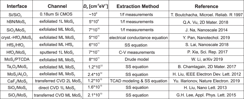
In Fig. 4a we compare typical transfer (ID–VG) characteristics measured for MoS2 FETs of different technologies14,40,46. Scaling EOT from 25 nm to 0.9–1.3 nm dramatically improves SS for all devices. However, a near-ideal SS of about 60 mV/dec has been obtained only for devices with exfoliated MoS2 using 1.3 nm EOT PTCDA/HfO2 insulators40, which is due to both the passivated interface of HfO2 by PTCDA and the low amount of channel defects in the exfoliated flakes. When using MoS2 channels grown by chemical vapour deposition (CVD) instead of exfoliated layers in otherwise identical devices, SS increases from 60 to 160 mV/dec40. Furthermore, MoS2 FETs with CVD-grown channels and 0.9 nm EOT CaF2 films46 also exhibited a SS of about 90 mV/dec. Thus, we argue that at the present level of 2D device technology, extracting Dit is not sufficient to assess the quality of the insulator surface in devices with CVD-grown channels, as Dit will be dominated by channel defects as well as adsorbates if the channel is not protected. In Fig. 4b we compare Dit values from literature (for more details see Box 1). Indeed, for all devices with CVD-grown channels46,73,74 Dit is close to 1013 cm−2 eV−1 compared to the 2 × 1012 cm−2 eV−1 of the unpassivated Si(100)/SiO2 interface which is reduced to below 1010 cm−2 eV−1 after annealing. Dit is further barely dependent on the gate insulator, which means that the quality of CVD samples must be improved including the optimization or avoidance of the transfer of grown films from other substrates to produce defect-free channels. Alternatively, other growth techniques of 2D materials may be introduced, such as magnetron sputtering75. However, most Dit values have been extracted from 2D FETs with exfoliated channels38,40,41,43,54,76,77, which typically contain a lower amount of channel defects and thus currently allow drawing better conclusions on the contribution of the insulator to the interface quality.

a Gate transfer characteristics of CVD-grown MoS2 FETs with 25 nm SiO214, 0.9 nm EOT CaF246, 1.3 nm EOT PTCDA/HfO240 and exfoliated devices of the latter technology40. b Comparison of Dit values measured for Si devices78 and different 2D technologies38,40,41,43,46,54,73,74,75,76,77. c Comparison of SS values for different 2D devices16,38,40,41,43,46,54,66 with EOT below 10 nm. For scaled insulators SS appears insensitive to further EOT scaling and mostly affected by the interface quality, which can be improved via the routes 1–4a. “Insulator/2D semiconductor” is for back-gated and “2D semiconductor/insulator” is for top-gated device configurations.
Still, most frequently extracted Dit values in exfoliated 2D FETs are still high and range from 5 × 10¹¹ to 1012 cm−2 eV−1 for both conventional high-k oxides grown by ALD38,40,76 and native oxides of 2D materials41,43 obtained by oxidation. While the best Dit values achieved for 2D devices with SiO2 are two orders of magnitude lower77 than that, one can expect that further improvements will be achieved for high-k oxides by optimizing the deposition processes. However, without proper passivation of interfaces40 it still appears challenging to reach values below 1010 cm−2 eV−1, since oxide dangling bonds cannot be removed completely and the precise control of amorphous surfaces is difficult. As for native oxides of 2D materials, this research is at an early stage and thus further process optimization is required to achieve the desired improvement of Dit. Consequently, the use of crystalline materials with well-defined and chemically inert van der Waals interfaces with 2D materials appears to be an ideal way forward. For instance, a Dit of 5 × 109 cm−2 eV−1 achieved for hBN/MoS2 devices54 is already comparable to Si technologies78.
In Fig. 4c we compare SS from literature for different 2D FETs with scaled gate insulators16,38,40,41,43,46,54,66. Although from Eq. (1) one would expect the best SS for devices with smallest EOT, in reality the situation is more complex. For instance, the use of crystalline 2D insulators54 or native 2D oxides41 coupled with contact engineering to reduce the Schottky barriers leads to a near-ideal SS already for an EOT of ~8 nm, and even for thicker hBN layers in WSe2 FETs if transferred via contacts and clean van der Waals integration processes are used79. Again, this currently appears to be possible only with exfoliated channels, while for devices with CVD-grown films SS can be far from its ideal values even for EOT close to 1 nm40,46. We conclude that the use of high-quality channels and insulators with well-defined surfaces or native interfaces is the most important requirement to reduce Dit and achieve near-ideal SS for 2D FETs with sub-1 nm EOT gate insulators. The latter can also include partially crystallized amorphous oxides, since their surface quality has been shown to considerably improve after annealing at high temperatures38.
In addition to their impact on SS, Dit also manifests as charged defects, which lead to scattering of carriers and in turn dramatically reduces their mobility. For instance, graphene on an SiO2 surface with its numerous dangling bonds has a mobility of between 1000 and 25,000 cm2/Vs80,81,82, which increases to 27,000–65,000 cm2/Vs82 on hBN substrates. Subsequently, hBN has been also shown to improve the mobility in MoS2 FETs11. Ionic crystals, such as CaF2 can also yield high-quality interfaces with 2D materials47,83,84 which should result in improved mobilities.
Border traps and device stability
Contrary to interface states, border traps49 are situated at a certain distance from the interface which allows charge exchange with the channel through tunneling processes. While interface states are typically very fast, border traps are much slower, with their capture (τc) and emission (τe) time constants depending on the distance from the interface and structural relaxation following charge trapping. The best studied insulators are SiO2 and HfO2, which contain intrinsic (mostly oxygen vacancies and trapping sites at strained bonds) as well as extrinsic (for instance caused by trapped hydrogen atoms) defects. As confirmed on both Si85 and 2D86,87 devices, the time constants of border traps in amorphous oxides are widely distributed (from below nanoseconds to many years), which is a fundamental property of amorphous materials. As for other insulators, the physical and chemical nature of the prevalent defects is much less understood. For instance, the possible intrinsic defects in hBN identified using theoretical methods88,89 are nitrogen and boron vacancies and anti-sites. However, it appears that in crystalline insulators the surrounding of each particular defect is much more uniform and regular which should lead to a much narrower distribution of the time constants. Recently this was confirmed by comparing the hysteresis dynamics in MoS2 FETs with SiO2 and hBN, as in the latter case the hysteresis width starts to decrease when using slow sweeps58.
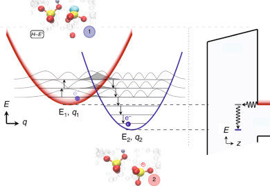
Since border traps can capture and emit carriers, they can cause various instabilities in the device characteristics (Fig. 5). The most widely observed issues in 2D devices are the hysteresis of the gate transfer characteristics11,12,45,54,58 and long-term drifts of the threshold voltage90,91,92, which are commonly known from Si technologies as BTI, given their strong bias and temperature dependence85. Recent analysis of experimental results for MoS258,70,71,93,94 and black phosphorus23,50 using non-radiative multiphonon (NMP) models95 (see more details in Box 2) suggests that hysteresis and BTI have the same microscopic origin and result from changes in the charge state of border traps (Fig. 5a). For instance, BTI degradation appears as a shift of the ID–VG characteristics after application of some gate bias stress VG for a certain stress time ts, which tends to recover when the stress is removed. Depending on the polarity of the applied VG during stress, the phenomenon is then referred to as either positive (PBTI) or negative (NBTI) and may result in different shifts of the ID–VG characteristics. Similarly, the hysteresis is a superposition of cumulative NBTI and PBTI shifts of Vth caused by charge trapping during ID–VG sweeps. As a result, there is a difference in Vth when measuring forward and reverse sweeps. Since border defects have widely distributed capture and emission times, the faster ones contribute to the hysteresis and the slower ones also to BTI. In particular, the strong gate bias dependence of the time constants71, which is typical for border traps, results in a sizeable hysteresis. Other issues caused by border traps include flicker (1/f) noise17,52, which appears as random fluctuations of ID (or, equivalently, Vth) and for nanoscale devices decomposes into discrete steps known as random telegraph noise (RTN)94,96, as well as hot-carrier degradation (HCD) during device operation at non-zero drain bias, which is also known from Si technologies97 and has been already observed for 2D devices98.

a Schematics of hysteresis and BTI in large-area 2D n-FETs, assuming one acceptor-type defect band in the insulator. The applied VG changes the number of charged defects by moving trap levels across the Fermi level, which changes not only the occupancy of the defects but also their time constants τc and τe. A negative VG brings more defects above the Fermi level and makes them neutral. This leads either to NBTI degradation after long stress or more negative Vth in the beginning of the forward ID–VG sweep. A positive VG brings more defects below EF and makes them negatively charged, thus causing PBTI degradation or more positive Vth in the end of the forward sweep and during the reverse ID-VG sweep. Thus BTI and hysteresis are both the result of an ensemble of defects with distributed τc(VG) and τe(VG). b Schematics of RTN in nanoscale 2D FETs, assuming one discrete defect in the channel. RTN is observed within a relatively narrow VG range when EF is close to the defect level. At more negative VG the defect is slightly above EF and thus mostly neutral. At more positive VG it is slightly below EF and thus mostly charged. Analysis of RTN traces measured at different VG and T allows to extract the τc(VG, T) and τe(VG, T) dependences, which contain information about energy level, depth in the insulator, and relaxation energy of the defect.
In Si technologies these instabilities are commonly referred to as reliability issues, since they have a pronounced impact on the device performance only after many hours or weeks of operation. However, in 2D devices the typical densities of border traps can be orders of magnitude larger. As a result, the impact of defects on the device performance is already noticable at time zero. In other words, like in SiC, GaN, and other III–V devices, charge trapping related issues become a stability problem. Also, it has to be kept in mind that it is not the actual number of defects present in an insulator which determines device stability, but rather the number of active defects, that is, those defects which can change their charge state during device operation.
The most important aspect which determines the intensity of charge trapping by border traps, and consequently the effective density of active defects Dot and the magnitude of the hysteresis and BTI, is their energetic alignment. In amorphous oxides, the defects are energetically aligned within certain defect bands which also have a sizeable width99,100. These defect bands are broadened if the surroundings of each defect varies, which is typical for amorphous materials. In the simplest case, defects can be either donor- (neutral or positive) or acceptor-like (neutral or negative). For donor-like states, if their thermodynamic trap level ET is above the Fermi level EF, they are unoccupied and thus positively charged, and neutral otherwise. For acceptor-like states, on the other hand, defects are neutral for ET > EF and negatively charged otherwise. In contrast to amorphous oxides, defects in crystalline insulators are expected to form much narrower defect bands (or even discrete defect levels) as has already been shown for hBN101. Note that the density of active defects is always smaller if the defect bands are energetically far from the conduction (for n-FETs) and valence (for p-FETs) bands of the channel, which can be considered a design option for 2D FETs, as discussed below.
The density of insulator defects within a certain defect band may depend on the material type, deposition technique, stoichiometry, and annealing conditions. However, neither in 3D nor in 2D devices with amorphous oxides can the density of border traps be minimized towards undetectable levels, and thus these defects will be present even in perfectly optimized devices. We expect this to also hold for devices with native oxides of 2D materials, which ideally should have lower Dit compared to standard oxides while still having a comparable density of border traps within their characteristic defect bands. In contrast, in 2D FETs with crystalline insulators the defect densities inside narrow defect bands are expected to be significantly reduced.
Independently of the insulator used, the total number of defects is proportional to the channel area. Thus, as the device dimensions are scaled down to sub-100 nm and higher quality insulators are used, only a few defects per channel will remain even for amorphous oxides. However, the impact of each particular defect is inversely proportional to the channel area and becomes stronger for scaled devices102. As a result, in nanoscale 2D FETs capture and emission of a single carrier can strongly perturb the electrostatics inside the channel and thus cause RTN fluctuations in ID and Vth. A few recent studies for MoS2 FETs94,96 have already established that in general the dynamics of RTN in 2D FETs are very similar to Si technologies103,104. For instance, it was demonstrated that charge trapping events causing RTN are the same as those responsible for the hysteresis and BTI94, with the unique characteristic of border traps being the exponential VG dependence of the time constants (Fig. 5b).
Dielectric strength and breakdown mechanisms
The dielectric strength is characterized by two main parameters. The first one is the breakdown field EBD, which is the electric field at which a complete failure of the insulator takes place. This typically depends on the material type, quality and stoichiometry105, and ideally should exceed 10 MV/cm for EOT below 1 nm. EBD can be obtained by applying current-voltage sweeps and extracting the voltage at which the leakage currents experience a large and irreversible increase of several orders of magnitude. The second parameter is the time to reach the time-dependent dielectric breakdown (TDDB)106 when the dielectric is exposed to a constant voltage stress.
Breakdown consists of the progressive microscopic degradation of a dielectric material when it is exposed to electrical stress. This stress results in: (i) breaking bonds in the dielectric (where oxygen vacancies commonly appear in metal oxides), and (ii) migration of ions from the adjacent electrodes into the dielectric. When the density of defects reaches a threshold, a conductive percolation path through the dielectric can be formed. In 3D oxides dielectric breakdown is more progressive for thinner dielectrics, while in 2D layered dielectrics it has been suggested to take place layer-by-layer107,108. However, this layer-by-layer breakdown has been only observed by conductive atomic force microscopy (CAFM), where the electric field is confined by a nanoscale tip, and should be confirmed for macroscopic devices.
It is worth noting that dielectric breakdown always takes place at the electrically weakest location of the dielectric. Preexisting defects can favor a wide range of unwanted charge transport phenomena, such as charge trapping and de-trapping (resulting in RTN), and after some time can trigger the formation of new defects in surrounding areas. At the device level this results in an increase of the leakage current called stress induced leakage current (SILC), which finally triggers dielectric breakdown. Therefore, the presence of local lattice distortions in 2D insulators is a very important source of non-idealities which can accelerate dielectric breakdown109. At the same time, the number of local defects in both 2D and 3D insulators depends strongly on the synthesis process used. In general, dielectric breakdown should be investigated with a statistically relevant experimental design.
Impact of mechanical strain
One very promising direction for the application of 2D devices is flexible electronics110. Thus, the impact of mechanical strain on the device performance can be a limiting factor specific to these applications. Previous studies on MoS2 FETs with hBN suggest that the performance of these devices is not affected by mechanical strain up to 1.5%11. In contrast, devices with Al2O3 insulators exhibit a sizable threshold voltage shift for a strain of only ~0.07%, which can also be exploited for applications as piezoresistive strain sensors111. This is in line with experimental reports on the relatively high piezoresistive gauge factor of TMDs like MoS2112 or PtSe2113. It appears that a strong impact of strain on the performance of the devices with amorphous oxides is related to the strain changing the bandgap of MoS2111, which affects the relative alignment of the defect bands to the conduction/valence band edges, and may also shift the Fermi level. This in turn changes the charge state of border traps near the interface and the density of active defects. Thus, crystalline insulators which contain a lower amount of defects appear to be more suitable candidates also for flexible electronics applications.
Future development of 2D electronics
Taking into account the current state-of-the-art discussed above, in the following we propose research strategies for the development of 2D devices with the three most important types of gate insulators, which are amorphous 3D oxides, native oxides of 2D semiconductors and crystalline insulators.
Devices with conventional 3D oxides
The main limitations for integration of 3D oxides into electronic devices based on 2D materials result from their poor interface quality as well as their wide defect bands and their respective energetic alignment with the conduction/valence bands of the channel. It is important to realize that only a joint solution for both issues can be considered a promising way forward. For instance, recent attempts to passivate oxide interfaces by using thin molecular crystals39,40 improve only the interface quality, while deposition of these materials in homogeneous layers may present a technological challenge. However, it appears to us that a complete passivation of the defect bands would require thicker seeding layers which are incompatible with the sub-1 nm EOT requirement. Thus, we argue that in addition to further process optimization and van der Waals integration of the interfaces, an important goal of future research on 3D oxides for 2D devices should be the selection of the most favourably matched 2D channel/3D oxide combinations. Namely, for p-FETs it is important to select an insulator with defect bands energetically far from the valence band of the channel, while for n-FETs they must be separated from the conduction band. As a result, the density of active border traps being able to contribute to charge trapping will be reduced, thus leading to more stable device operation. The energetic alignment of defect bands can be extracted either by fitting TCAD models to measured stability characteristics of 2D devices23,71 or by using experimental methods such as the incremental hysteresis sweep method50,93 or trap spectroscopy methods previously developed for Si devices99.
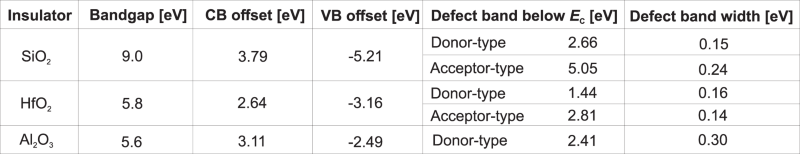
For the most relevant oxides (SiO2, HfO2, Al2O3), defect bands have already been extracted for Si devices99,114 as well as for 2D FETs23,71,93 and reconfirmed for different technologies. In Fig. 6 we show the energetic alignments of known defect bands in oxides relative to the band edges of graphene, BP and the most commonly used TMD channel materials. While the defects responsible for these bands can be considered a fundamental property of the insulator, the parameters of the defect bands vary weakly with the processing conditions114. Even though some materials may contain additional but currently unknown defect bands, some competitive combinations of insulators and 2D channels (e.g. Al2O3 on BP for p-FETs and perhaps HfO2 on MoS2 for n-FETs) can be preselected based on Fig. 6. Furthermore, another degree of freedom is the adjustable number of layers in a 2D channel, which affects the bandgap and thus may allow tuning the relative alignment of the channel band edges and defect bands in the insulator.

Left: energetic alignments of already known defect bands (gray areas) in several 3D oxides23,93,99,114 relative to the conduction and valence band edges of some frequently used 2D channel materials157 (center). Right: matching of potentially interesting native oxides, ionic crystals and 2D insulators with the same 2D channels. Note that HfO2 can be both a 3D oxide and the native oxide of HfS2 and HfSe2 and might have similar defect bands in both cases. The dielectric constants are given next to the valence band of the insulators while the numerical values are summarized in tabular form in Box 3. The zero energy would correspond with the Si midband.
Integrating 3D oxides with 2D materials by van der Waals forces can be achieved by passivating the 2D surfaces with molecular crystals. While this approach appears promising, it requires further investigations as this step may introduce additional limitations, such as poor dielectric strength of the seeding layer, insufficient barrier heights, low adhesion, and eventually a significant increase in EOT.
An alternative design route would be the creation of clean and stable oxide surfaces first, although in our opinion this is challenging for all previously discussed 3D oxides, in part due to their chemical reactivity. In theory, this problem can be solved by using an inverse design approach115, where the desired functionality (e.g. smooth interface) is declared first, and ab initio modeling is then performed to predict which stable and synthesizable materials would exhibit the required properties. These predictions can be based on genetic algorithms116 that identify materials with target properties while allowing deviations. In addition to predicting 3D oxides with smooth interfaces, we suggest that the same approach can be used to identify which new compounds will have the most suitable dielectric properties and targeted energetic alignments of defect bands. Finding ideal insulators therefore requires at least three coupled criteria, i.e. dielectric properties, interface quality and defect bands, and result in the required chemical formula. Once a new material is synthesized, extensive experimental characterization will still be required with respect to all important parameters. However, we expect the probability of finding 3D oxide compounds which would simultaneously satisfy all necessary requirements and could be easily synthesizable to be rather small. Instead, we propose a combination of theory and experiments to investigate alternative insulators for 2D electronics in the near future.
Devices with native oxides of 2D materials
The use of native oxides of 2D semiconductors41,42,43,44 is a promising way to overcome the limitations of 3D oxides as they may lead to improved interface quality. Among the materials which have already been investigated as gate insulators in 2D devices, we mention Ta2O5, which can be thermally oxidized from TaS241, and HfO2, which can be obtained by ambient exposure of HfSe242 or by plasma oxidation of HfS243. This field is relatively unexplored, and in many cases the oxidation of 2D semiconductors leads to the formation of non-stoichiometric metal oxides, such as HfOx for HfS244.
Nevertheless, we think that the integration of non-stoichiometric oxides into 2D devices could be of interest, as it allows tuning the charge carrier concentration in the channel through charge transfer doping, where the doping concentration can be varied by changing the oxygen content x105,117. Thus, it might be possible to vary the oxygen content of the native oxide using inverse design algorithms115 to possibly predict the compounds with desired functionality. One technological option is plasma oxidation of multi-layer WSe2 which leads to the formation of the native oxide WOx and efficient p-doping of WSe2 FETs118. It has further been shown that WOx and MoOx, a native oxide of MoS2, can be obtained by various oxidation methods without damaging the underlying 2D material119,120. However, the use of these native oxides as gate insulators in 2D devices has not been demonstrated so far. On the other hand, AlOx encapsulation layers121 and HfOx gate insulators117 have been used to dope MoS2 FETs, even though these oxides are not native for MoS2. The stoichiometric native oxides WO3 and MoO3 have been known for a long time122,123 and also appear promising for WSe2 and MoS2 FETs. While each 2D material normally has only one native oxide, some 2D semiconductors (e.g. MoS2) can be also matched with native oxides of other materials (e.g. Ta2O5)41. However, recent studies suggest that some of these materials, as well as Ta2O5, have rather narrow bandgaps124, and exhibit unfavourable band offsets with such widely used 2D semiconductors as MoS2 (Fig. 6).
In addition, these native 2D oxides are still amorphous and will therefore contain distinct defect bands. Furthermore, the non-stoichiometric ones are expected to exhibit very high defect densities and limited dielectric strength105. Thus, as well as for 3D oxides, we suggest that decreasing the number of active defects will present a challenge, and the locations of the defect bands are currently unknown for most of these materials.
Overall, the true potential of native oxides for 2D devices remains to be explored and the research in this field is now in an early stage. While theoretical predictions may provide some guidelines, we suggest that many technological issues remain with respect to fully scalable integration and controllable quality, as there is currently no clear recipe on how to achieve the ultimate goal of minimized or even completely eliminated defect bands. Furthermore, all native oxides except HfO2 do not seem to be competitive with respect to their dielectric properties, which could make them applicable only as passivation layers124. Thus, in the following section we discuss insulators which could retain their crystalline structure even when fabricated as ultra-thin layers.
Devices with crystalline insulators
Crystalline materials theoretically provide the largest potential for obtaining defect-free insulators and overcoming problems associated with both interface quality and defect bands. The most promising results for 2D FETs have recently been obtained for crystalline layered 2D insulators, in particular hBN108,125 and mica126, as well as the ionic crystal CaF246,62,127,128. These materials and some other known fluorides are summarized in Fig. 6.
The most widely studied crystalline insulator for 2D materials is hBN11,45,54,58. Devices using hBN typically exhibit a sizable improvement in terms of SS54 and mobility11 and also show considerably reduced charge trapping compared to 3D oxides45,58. This can be explained by the well-defined surface of hBN and the low density of border traps in this crystalline material. Unfortunately, hBN has mediocre dielectric properties, such as a rather narrow bandgap of about 6 eV129, a small dielectric constant of 5.06130, and unfavourable band offsets to most 2D materials (see Fig.6). As scaled FET technologies require an EOT below 1 nm (corresponding to a physical hBN thickness of below 1.3 nm), hBN is expected to result in excessive thermionic and direct tunneling leakage currents potentially orders of magnitude larger than those expected for high-k oxides. However, the exact nature of leakage currents across monolayer and multilayer hBN as well as the impact of the van der Waals gap is still not fully understood. As an example, it has been recently reported68 that Ti/hBN(5–6 nm)/Au structures exhibit leakage currents surprisingly lower than much thicker Pt/SiOxNy:Ag(50 nm)/Pt131 structures.
Knowledge regarding the dielectric strength of hBN as well as its breakdown mechanisms is also very scarce. Previous studies have been conducted mostly at the material-level107,108 and metal-insulator-metal device configurations (e.g. memristors132). It has been shown that thick (>10 nm) multilayer hBN stacks obtained by mechanical exfoliation experience a layer-by-layer breakdown107,108 when exposed to high electric fields. However, at the device level native defects in hBN, such as nitrogen and boron vacancies and antisites predicted by DFT modeling88,89, are expected to mask this phenomenon, leading to a more progressive breakdown process109.
More experiments are required to clarify the dielectric properties and the breakdown behavior of hBN stacks in FETs to fully understand the potential of hBN for ultra-scaled digital 2D devices. Nevertheless, it can already be concluded that hBN is indeed a promising insulator for analog 2D devices that do not require aggressive thickness scaling and operate at low electric fields, such as photodetectors35 and sensors36 employing graphene channels.
Mica is another interesting layered 2D insulator that has been investigated as a back-gate insulator in GFETs126 and top-gate insulator in MoS2 FETs133. In addition to having a well-defined surface, this 2D insulator has a reasonably high permittivity (8.1) and a wide bandgap (10.5 eV), which would address some of the limitations of hBN. However, the studies performed on exfoliated flakes do not yet allow to assess the real potential of mica. It is worth noting that mica may be used as a growth substrate for other 2D materials, and thus lend itself to future integration schemes134. Other potentially interesting 2D insulators include crystalline Ti0.9O2135, 2D silicon dioxide136 and other atomically thin oxides137, although all these materials are still far from being integrable with conventional silicon technology.
3D ionic crystals possess well-defined surfaces and are hence discussed here. In our opinion, the most promising candidates for applications as gate insulators are epitaxial fluorides which form a wide class of different insulators and other emerging materials138. Many fluoride insulators have competitive dielectric properties, chemically inert surfaces, low density of insulator defects and high electric stability, which makes them highly suitable for 2D electronics. Recently it has been shown that competitive MoS2 FETs can be created using epitaxial CaF2 insulators of only 2 nm thickness46. Such thicknesses are currently barely achievable with 3D oxides owing to their poor amorphous quality. Remarkably, CaF2 is also competitive with high-k oxides in terms of its dielectric properties (e.g. wide bandgap of 12.1 eV and reasonably high dielectric constant of 8.43). In addition, it has been known for some time that CaF2 can form a well-defined van der Waals interface with 2D channels47. This feature allows heteroepitaxy of 2D materials on CaF2(111)83,84, thus opening additional opportunities for the creation of scalable 2D devices. Owing to the high crystalline quality of CaF2 insulators, MoS2 FETs on CaF2/Si(111) substrates were found to be extremely stable with respect to charge trapping46. At the same time, the analysis of breakdown in CaF2 using CAFM suggests that this material is highly homogeneous and has a very high dielectric strength.
These promising early results lead us to conclude that close attention should be paid also to other fluoride insulators such as LaF3, MgF2, BaF2, SrF2, and many others. Similarly to CaF2, many of these materials have very wide bandgaps (e.g. 11.4 eV for SrF2 and 13 eV for MgF2) but at the same time mediocre dielectric constants (e.g. 6.4 for SrF2 and 5.4 for MgF2). Nonetheless, for CaF2 theoretically predicted (Fig.3b) and measured (Fig.3c) leakage currents are still comparable to high-k oxides like HfO2, since the band offsets to Si and 2D semiconductors are high. However, for other fluorides possible limitations which may arise from their relatively low dielectric constants still have to be understood by performing electrical characterization of thin layers. Apart from 2D FETs, ionic crystals can be also of interest for analog 2D devices and other applications. For instance, the performance of 2D-based photodetectors35 strongly depends on the insulator properties and can be adjusted by choosing appropriate insulators. Also, the exciton properties (e.g. radiative lifetime) in excitonic devices139 strongly depend on the thickness and type of the insulator matched with the 2D material. However, at the present early stage of research it is not possible to make a final conclusion on the future potential of ionic fluoride crystals as their fundamental properties (e.g. chemical structure and breakdown mechanisms) are not well understood and thus require further in-depth studies. Furthermore, the compatibility of positive ions such as Ca2+ or Mg2+ with CMOS and possibly future beyond-CMOS technologies will have to be assessed by the community.
In addition to their use as insulators, the wide class of epitaxial fluorides138 also contains numerous materials with other fascinating properties. These are, for instance, antiferromagnetic NiF2140 and MnF2141, diamagnetic ZrF2141 and ferroelectric BaMgF4142. One of the most promising research directions is the use of ferroelectric BaMgF4142 in steep slope devices such as negative capacitance (NC) FETs, which could be game-changers for future low-power electronics. Previously reported NC FETs with MoS2 employed hafnium zirconium oxide (HZO)32,33, polymers143 and layered CuInP2S6 (CIPS)144 ferroelectrics. The best SS reported for devices with HZO approach 6 mV/dec at room temperature32. Although HZO appears more technologically relevant because of its CMOS compatibility and large area fabrication possibilities, we expect that some of these devices (e.g. HZO/Al2O3/MoS2 NC-FETs) will likely face the same problems with poor quality interfaces and border traps as standard 2D FETs. Thus, it is tempting to project that the use of BaMgF4, which has already been applied in ferroelectric Si-based devices145, will allow overcoming already achieved SS values while also leading to improved device stability. As a final comment, it is worth pointing out that the potential of NC-FET technologies is currently under debate by the community, since some studies suggest that the NC effect would not benefit devices that already have strong electrostatics, such as 2D FETs146.
Overall, it appears to us that crystalline insulators are currently the most promising materials for applications in various devices based on 2D materials, since their possible physical limitations appear easier to address than in amorphous oxides. Even at the present stage of research, the technological limitations of the currently used insulators are apparent. For instance, most devices with hBN and other layered 2D insulators employ tens of nanometers thick layers deposited by mechanical exfoliation. At the same time, attempts at scalable growth of hBN using CVD147 and MBE148 have not resulted in superior device performance than conventional 3D oxides149. Thus, fully scalable methods to grow layered 2D insulators have to be further developed. In the case of hBN, this currently involves temperatures above 800 °C150, which is far above the maximum allowed by the thermal budget of CMOS technologies (about 450 °C) for back end of line integration151. In contrast, for CaF2 and some other related insulators fully scalable MBE growth techniques partially exist, while the optimal growth temperatures for a few nanometer thick layers on Si appear more reasonable. For instance, MBE growth of CaF2 films at 250 °C results in high crystalline quality and pinhole-free layers46,152. Also, MBE growth of 2D semiconductors (e.g. MoSe2 and MoTe2) on CaF2(111) is possible at temperatures below 400 °C83,84. Furthermore, it is possible that heteroepitaxy of CaF2 and other related insulators (e.g. SrF2, MgF2, BaF2) on top of 2D semiconductors will be also possible at moderate growth temperatures. While for now a considerable limitation of ionic crystals is that they have been used only as a back-gate insulators46, we think that the latter requires more attention as this would allow obtaining Si/fluoride/2D/fluoride heterostructures as required for top-gated 2D FETs which is essential for integrated circuits.
Conclusions and outlook
Since 2004, when the field effect in graphene was reported for the first time153, many devices with different 2D materials have been demonstrated. The most prevalent among them are FETs with semiconducting 2D channels, which could be important building blocks for future post-silicon electronics. Owing to the thin body of 2D materials, their use as channels in FETs would allow suppressing the well-known short-channel effect of Si transistors, thus opening a route towards sub-5 nm device dimensions and prolonging Moore’s law154. Despite these high expectations and the progress made thus far, over a decade of intensive research has not led to a commercial 2D device technology155,156. One important reason discussed here is the lack of insulators suitable for integration into fully scalable 2D process flows, which would enable a competitive device performance and stability.
Most 2D FET prototypes reported in literature have been made using tens of nanometers thick oxide insulators, with no clear strategy on how to scale them down to sub-1 nm EOT as required for commercially competitive FETs. Thus, we firmly believe that the primary challenge is to identify fully scalable insulators for 2D FETs and to collect in-depth information about their properties. When considering a certain insulator as a potential candidate for integration into 2D technologies, its dielectric properties have to be identified first, as they are important for low gate leakage currents in scaled devices. Then, information about the quality of the interface between the insulator and 2D materials has to be gathered. This is required because a large amount of interface states, such as oxide dangling bonds, will result in poor device performance. Finally, attention has to be paid to the location and density of its defect bands, as well as their energetic alignment to various channel materials and possible mechanisms for the creation of new insulator defects under electric stress. This information is essential for further improving the stability and dielectric strength of 2D FETs. This is an important aspect, because although considerable progress has been made in optimizing 2D device performance, the stability of 2D FETs and analog devices is far from being competitive with Si technologies and remains poorly understood.
2D devices and their technology face enormous challenges towards commercial uptake, and we have identified the search for a perfectly matching insulator/semiconductor combination as particularly urgent. This is because from the myriad of possible material combinations the right choice has to be made at as early a stage as possible by considering their scaling potential. Based on this observation, several new research problems can be formulated. First of all, research on high-k oxides as potentially interesting insulators for 2D devices should be continued, even though at present the problem of how to fabricate a clean interface to 2D materials presents an enormous challenge. Here, efforts related to improving the interface quality of 3D oxides by rapid thermal annealing38 and further development of native oxides41,42,43,44 of 2D semiconductors should be continued. Also, the correlation between growth conditions and their fundamental defect bands must be further explored. Next, we feel that two alternative directions for 2D FET technologies appear promising: The first alternative is the use of layered 2D insulators which produce near-perfect interfaces with 2D channels. One of these materials is hBN, but more investigations are required to clarify several unique properties of this dielectric, such as plane-to-plane interactions and electron tunneling across van der Waals structures. We further hope that this review triggers a more intensive search for other 2D insulators, such as mica and 2D oxide nanosheets. The second alternative is the use of ionic crystals such as fluorides, which create near-perfect van der Waals interfaces with 2D channels and simultaneously have good dielectric properties. Up to now, only CaF2 has been used as an insulator for 2D FETs46. However, the recent demonstration of epitaxial growth of 2D materials on CaF283,84 has opened a potential route to very large scale integration and perhaps to the development of 2D FETs based on fluoride/2D/fluoride heterostructures. Furthermore, there are many fluorides beyond CaF2 with fascinating properties as insulators or as magnetic and ferroelectric materials, which should in future allow to create more competitive 2D devices beyond FETs.
To conclude, the identification of the best insulators for 2D electronics presents an important roadblock of modern nanoscience and the apparent lack of information related to this problem should no longer be ignored. We are confident that further development of this research topic will sooner or later enable 2D electronics for commercial applications.
References
Huff, H. R. Integrated Circuits and nano-technology: a historical review. ECS Trans. 72, 275–287 (2016).
Vickridge, I., Ganem, J., Hoshino, Y. & Trimaille, I. Growth of SiO2 on SiC by dry thermal oxidation: mechanisms. J. Phys. D: Appl. Phys. 40, 6254 (2007).
Kamata, Y. High-k/Ge MOSFETs for future nanoelectronics. Mater. Today 11, 30–38 (2008).
DelAlamo, J. A. Nanometre-scale electronics with III–V compound semiconductors. Nature 479, 317 (2011).
Gila, B. P. et al. Gadolinium oxide and scandium oxide: gate dielectrics for GaN MOSFETs. Phys. Status Solidi (a) 188, 239–242 (2001).
Hu, J., Saraswat, K. C. & Wong, H.-S. P. Metal/III-V Schottky Barrier height tuning for the design of nonalloyed III-V field-effect transistor source/drain contacts. J. Appl. Phys. 107, 063712 (2010).
Chang, L. et al. Extremely scaled silicon nano-CMOS devices. Proc. IEEE. 91, 1860–1873 (2003).
Uchida, K. et al. Experimental study on carrier transport mechanism in ultrathin-body SOI n- and p-MOSFETs with SOI thickness less than 5 nm, 47-50 (IEEE, IEDM 2002).
Schmidt, M. et al. Mobility extraction in SOI MOSFETs with sub 1 nm body thickness. Solid-State Electron 53, 1246–1251 (2009).
Radisavljevic, B., Radenovic, A., Berivio, J., Giacometti, V. & Kis, A. Single-layer MoS2 transistors. Nat. Nanotechnol. 6, 147–150 (2011).
Lee, G.-H. et al. Flexible and transparent MoS2 field-effect transistors on hexagonal boron nitride-graphene heterostructures. ACS Nano 7, 7931–7936 (2013).
Cho, A.-J. et al. Multi-layer MoS2 FET with small hysteresis by using atomic layer deposition Al2O3 as gate insulator. ECS Solid State Lett. 3, Q67–Q69 (2014).
Guo, Y. et al. Charge trapping at the MoS2-SiO2 interface and its effects on the characteristics of MoS2 metal-oxide-semiconductor field effect transistors. Appl. Phys. Lett. 106, 103109 (2015).
Illarionov, Y. et al. Improved hysteresis and reliability of MoS2 transistors with high-quality CVD growth and Al2O3 encapsulation. IEEE Electron Device Lett. 38, 1763–1766 (2017).
Smithe, K., Suryavanshi, S., Munoz-Rojo, M., Tedjarati, A. & Pop, E. Low variability in synthetic monolayer MoS2 devices. ACS Nano 11, 8456–8463 (2017).
Bolshakov, P. et al. Improvement in top-gate MoS2 transistor performance due to high quality backside Al2O3 layer. Appl. Phys. Lett. 111, 032110 (2017).
Liao, W., Wei, W., Tong, Y., Chim, W. K. & Zhu, C. Electrical performance and low frequency noise in hexagonal boron nitride encapsulated MoSe2 dual-gated field effect transistors. Appl. Phys. Lett. 111, 082105 (2017).
Chang, Y.-M. et al. Reversible and precisely controllable p/n-type doping of MoTe2 transistors through electrothermal doping. Adv. Mater. 30, e1706995, (2018).
Aji, A. S., Solís-Fernández, P., Ji, H. G., Fukuda, K. & Ago, H. High mobility WS2 transistors realized by multilayer graphene electrodes and application to high responsivity flexible photodetectors. Adv. Fun. Mater. 27, 1703448 (2017).
Allain, A. & Kis, A. Electron and hole mobilities in single-layer WSe2. ACS Nano 8, 7180–7185 (2014).
Wood, J. et al. Effective passivation of exfoliated black phosphorus transistors against ambient degradation. Nano Lett. 14, 6964–6970 (2014).
Kim, J.-S. et al. Toward air-stable multilayer phosphorene thin-films and transistors. Sci. Rep. 5, 1–7 (2015).
Illarionov, Y. et al. Long-term stability and reliability of black phosphorus field-effect transistors. ACS Nano 10, 9543–9549 (2016).
Geim, A. & Grigorieva, I. Van der Waals heterostructures. Nature 499, 419–425 (2013).
AlMutairi, A. A., Zhao, Y., Yin, D. & Yoon, Y. Performance limit projection of germanane field-effect transistors. IEEE Electron Device Lett. 38, 673–676 (2017).
Bonaccorso, F. et al. Production and processing of graphene and 2d crystals. Mater. Today 15, 564–589 (2012).
English, C., Shine, G., Dorgan, V., Saraswat, K. & Pop, E. Improved contacts to MoS2 transistors by ultra-high vacuum metal deposition. Nano Lett. 16, 3824–3830 (2016).
Smithe, K., English, C., Suryavanshi, S. & Pop, E. Low variability in synthetic monolayer MoS2 devices. 2D Mater. 4, 011009 (2017).
Pei, T. et al. Few-layer SnSe2 transistors with high on/off ratios. Appl. Phys. Lett. 108, 053506 (2016).
Roy, T. et al. Dual-gated MoS2/WSe2 van der Waals tunnel diodes and transistors. ACS Nano 9, 2071–2079 (2015).
Wang, X. et al. Ferroelectric FET for nonvolatile memory application with two-dimensional MoS2 channels. 2D Mater. 4, 025036 (2017).
McGuire, F. et al. Sustained sub-60 mV/decade switching via the negative capacitance effect in MoS2 transistors. Nano Lett. 17, 4801–4806 (2017).
Si, M. et al. Steep-slope hysteresis-free negative capacitance MoS2 transistors. Nat. Nanotechnol. 13, 24–28 (2018).
Mohsin, M. et al. Graphene based low insertion loss electro-absorption modulator on SOI waveguide. Opt. Expr. 22, 15292–15297 (2014).
Koppens, F. et al. Photodetectors based on graphene, other two-dimensional materials and hybrid systems. Nat. Nanotechnol. 9, 780 (2014).
Hess, L. H. et al. Graphene transistor arrays for recording action potentials from electrogenic cells. Adv. Mater. 23, 5045–5049 (2011).
Lemme, M., Echtermeyer, T., Baus, M. & Kurz, H. A graphene field effect device. IEEE Electron Device Lett. 27, 1–12 (2007).
Pan, Y. et al. Near-ideal subthreshold swing MoS2 back-gate transistors with an optimized ultrathin HfO2 dielectric layer. Nanotechnology 30, 095202 (2019).
Park, J. H. et al. Atomic layer deposition of Al2O3 on WSe2 functionalized by titanyl phthalocyanine. ACS Nano 10, 6888–6896 (2016).
Li, W. et al. Uniform and ultrathin high-κ gate dielectrics for two-dimensional electronic devices. Nat. Electron. 2, 563–571 (2019).
Chamlagain, B. et al. Thermally oxidized 2D TaS2 as a high-κ gate dielectric for MoS2 field-effect transistors. 2D Mater. 4, 031002 (2017).
Mleczko, M. J. et al. HfSe2 and ZrSe2: two-dimensional semiconductors with native high-κ oxides. Sci. Adv. 3, e1700481 (2017).
Lai, S. et al. HfO2/HfS2 hybrid heterostructure fabricated via controllable chemical conversion of two-dimensional HfS2. Nanoscale 10, 18758–18766 (2018).
Peimyoo, N. et al. Laser-writable high-k dielectric for van der waals nanoelectronics. Sci. Adv. 5, eaau0906 (2019).
Lee, C. et al. Comparison of trapped charges and hysteresis behavior in hBN encapsulated single MoS2 flake based field effect transistors on SiO2 and hBN substrates. Nanotechnology 29, 335202 (2018).
Illarionov, Y. et al. Ultrathin calcium fluoride insulators for two-dimensional field-effect transistors. Nat. Electron. 2, 230–235 (2019).
Koma, A., Saiki, K. & Sato, Y. Heteroepitaxy of a two-dimensional material on a three-dimensional material. Appl. Surf. Sci. 41, 451–456 (1990).
Robertson, J. High dielectric constant oxides. Eur. Phys. 28, 265–291 (2004).
Fleetwood, D. Border traps in MOS devices. Nucl. Sci. 39, 269–271 (1992).
Illarionov, Y. et al. Highly-stable black phosphorus field-effect transistors with low density of oxide traps. npj 2D Mater. Appl 1, 23 (2017).
Grandchamp, B. et al. Characterization and modeling of graphene transistor low-frequency noise. Electron Dev. 59, 516–519 (2012).
Nie, X.-R. et al. Thickness dependence of low-frequency noise in MoS2 field-effect transistors with enhanced back-gate control. IEEE Electron Dev. Lett. 39, 739–741 (2018).
DiBartolomeo, A. et al. Hysteresis in the transfer characteristics of MoS2 transistors. 2D Mater. 5, 015014 (2017).
Vu, Q. et al. Near-zero hysteresis and near-ideal subthreshold swing in h-BN encapsulated single-Layer MoS2 field-effect transistors. 2D Mater. 5, 031001 (2018).
Grasser, T. Bias Temperature Instability for Devices and Circuits. (Springer Science & Business Media, 2013)
Register, L. F., Rosenbaum, E. & Yang, K. Analytic model for direct tunneling current in polycrystalline silicon-gate metal–oxide–semiconductor devices. Appl. Phys. Lett. 74, 457–459 (1999).
Vexler, M. I. et al. A general simulation procedure for the electrical characteristics of metal-insulator-semiconductor tunnel structures. Semiconductors 47, 686–694 (2013).
Illarionov, Y. et al. The role of charge trapping in MoS2/SiO2 and MoS2/hBN field-effect transistors. 2D Mater. 3, 035004 (2016).
Brar, B., Wilk, G. & Seabaugh, A. Direct extraction of the electron tunneling effective mass in ultrathin SiO2. Appl. Phys. Lett. 69, 2728–2730 (1996).
Guha, S. et al. High-quality aluminum oxide gate dielectrics by ultra-high-vacuum reactive atomic-beam deposition. J. Appl. Phys. 90, 512–514 (2001).
Iwai, H. et al. Advanced gate dielectric materials for sub-100 nm CMOS, 625–628 (IEEE IEDM, 2002).
Vexler, M., Illarionov, Y., Suturin, S., Fedorov, V. & Sokolov, N. Tunneling of electrons with conservation of the transverse wave vector in the Au/CaF2/Si(111) system. Phys. Solid State 52, 2357–2363 (2010).
Britnell, L. et al. Electron tunneling through ultrathin boron nitride crystalline barriers. Nano Lett. 12, 1707–1710 (2012).
Zou, X. et al. Interface engineering for high-performance top-gated MoS2 field-effect transistors. Adv. Mater. 26, 6255–6261 (2014).
Jeong, S.-J. et al. Thickness scaling of atomic-layer-deposited HfO2 films and their application to wafer-scale graphene tunnelling transistors. Sci. Rep. 6, 20907 (2016).
Wang, X. et al. Improved integration of ultra-thin high-k dielectrics in few-layer MoS2 FET by remote forming gas plasma pretreatment. Appl. Phys. Lett. 110, 053110 (2017).
Gottlob, H. D. B. et al. CMOS integration of epitaxial Gd2O3 high-k gate dielectrics. Solid State Electron 50, 979–985 (2006).
Shi, Y. et al. Electronic synapses made of layered two-dimensional materials. Nat. Electron 1, 458 (2018).
Sarkar, D. et al. A subthermionic tunnel field-effect transistor with an atomically thin channel. Nature 526, 91 (2015).
Knobloch, T. et al. Impact of gate dielectrics on the threshold voltage in MoS2 transistors. ECS Trans. 80, 203–217 (2017).
Knobloch, T. et al. A physical model for the hysteresis in MoS2 transistors. IEEE J. Electron Dev. Soc. 6, 972–978 (2018).
Appenzeller, J., Zhang, F., S., Das & J., Knoch 2D materials for nanoelectronics. 2D Mater. Nanoelectronics 17, 207–234 (2016).
Liu, H. et al. Statistical study of deep submicron dual-gated field-effect transistors on monolayer chemical vapor deposition molybdenum disulfide films. Nano Lett. 13, 2640–2646 (2013).
Lee, C. H. et al. Transferred large area single crystal MoS2 field effect transistors. Appl. Phys. Lett. 107, 193503 (2015).
Xia, P. et al. Impact and origin of interface states in MOS capacitor with monolayer MoS2 and HfO2 High-k dielectric. Sci. Rep. 7, 40669 (2017).
Liu, H. & Ye, P. MoS2 dual-gate MOSFET with atomic-layer-deposited Al2O3 as top-gate dielectric. IEEE Electron Device Lett. 33, 546–548 (2012).
Na, J. et al. Low-frequency noise in multilayer MoS2 field-effect transistors: the effect of high-k passivation. Nanoscale 6, 433–441 (2014).
Boutchacha, T., Ghibaudo, G., Guegan, G. & Skotnicki, T. Low frequency noise characterization of 0.18 μm Si CMOS transistors. Microelectron. Reliab 37, 1599–1602 (1997).
Jung, Y. et al. Transferred via contacts as a platform for ideal two-dimensional transistors. Nat. Electron. 2, 187 (2019).
Taychatanapat, T. & Jarillo-Herrero, P. Electronic transport in dual-gated bilayer graphene at large displacement fields. Phys. Rev. Lett. 105, 166601 (2010).
Wang, H. et al. BN/graphene/BN transistors for RF applications. IEEE Electron Device Lett. 32, 1209–1211 (2011).
Petrone, N. et al. Chemical vapor deposition-derived graphene with electrical performance of exfoliated graphene. Nano Lett. 12, 2751–2756 (2012).
Vishwanath, S. et al. Comprehensive structural and optical characterization of MBE grown MoSe2 on graphite, CaF2 and graphene. 2D Mater. 2, 024007 (2015).
Vishwanath, S. et al. MBE growth of few-layer 2H-MoTe2 on 3D substrates. J. Cryst. Growth 482, 61–69 (2018).
Grasser, T. et al. Analytic Modeling of the Bias Temperature Instability Using Capture/Emission Time Maps, 27.4.1–27.4.4. (IEEE IEDM, 2011)
Illarionov, Y. et al. Bias-Temperature Instability in Single-Layer Graphene Field-Effect Transistors: a Reliability Challenge. in Proc. 2014 IEEE Silicon Nanoelectronics Workshop, 29–30 (IEEE, 2014).
Illarionov, Y. et al. Bias-temperature instability in single-layer graphene field-effect transistors. Appl. Phys. Lett. 105, 143507 (2014).
Azevedo, S., Kaschny, J. R., de Castilho, C. M. C. & de Brito Mota, F. A theoretical investigation of defects in a boron nitride monolayer. Nanotechnology 18, 495707 (2007).
Matos, M. J. S., Mazzoni, M. S. C. & Chacham, H. Graphene–boron nitride superlattices: the role of point defects at the BN layer. Nanotechnology 25, 165705 (2014).
Yang, S., Park, S., Jang, S., Kim, H. & Kwon, J.-Y. Electrical stability of multilayer MoS2 field-effect transistor under negative bias stress at various temperatures. Phys. Status Solidi 8, 714–718 (2014).
Illarionov, Y. et al. Bias-temperature instability on the back gate of single-layer double-gated graphene field-effect transistors. Jpn. J. Appl. Phys. 55, 04EP03 (2016).
Kim, T.-Y. et al. Electrical properties of synthesized large-area MoS2 field-effect transistors fabricated with inkjet-printed contacts. ACS Nano 10, 2819–2826 (2016).
Illarionov, Y. et al. Energetic mapping of oxide traps in MoS2 field-effect transistors. 2D Mater. 4, 025108 (2017).
Stampfer, B. et al. Characterization of single defects in ultra-scaled MoS2 field-effect transistors. ACS Nano 12, 5368–5375 (2018).
Alkauskas, A., Yan, Q. & Van de Walle, C. G. First-principles theory of nonradiative carrier capture via multiphonon emission. Phys. Rev. B 90, 075202 (2014).
Nan, F., Nagashio, K. & Toriumi, A. Experimental detection of active defects in few layers MoS2 through random telegraphic signals analysis observed in its FET characteristics. 2D Mater. 4, 015035 (2016).
Procel, L. M., Crupi, F., Franco, J., Trojman, L. & Kaczer, B. Defect-centric distribution of channel hot carrier degradation in nano-MOSFETs. IEEE Electron Device Lett. 35, 1167–1169 (2014).
Illarionov, Y. et al. Hot carrier degradation and bias-temperature instability in single-layer graphene field-effect transistors: similarities and differences. Electron Dev. 62, 3876–3881 (2015).
Degraeve, R. et al. Trap Spectroscopy by Charge Injection and Sensing (TSCIS): A Quantitative Electrical Technique for Studying Defects in Dielectric Stacks, 1–4. IEEE IEDM, 2008)
Franco, J.et al. Superior NBTI Reliability of SiGe Channel pMOSFETs: ReplacementGate, FinFETs, and Impact of Body Bias, 18.5.1–18.5.4. IEEE IEDM, 2011)
McDougall, N. L., Partridge, J. G., Nicholls, R. J., Russo, S. P. & McCulloch, D. G. Influence of point defects on the near edge structure of hexagonal boron nitride. Phys. Rev. B 96, 144106 (2017).
Kirton, M. & Uren, M. Noise in solid-state microstructures: a new perspective on individual defects, interface states and low-frequency (1/f) noise. Adv. Phys. 38, 367–468 (1989).
Cho, H.-J., Lee, S., Park, B.-G. & Shin, H. Extraction of trap energy and location from random telegraph noise in gate leakage current (Ig RTN) of metal-oxide semiconductor field effect transistor (MOSFET). Solid State Electron. 54, 362–367 (2010).
Hsieh, E., Tsai, Y., Chung, S., Tsai, C., Huang, R. & Tsai, C. The Understanding of Multi-level RTN in Trigate MOSFETs Through the 2D Profiling of Traps and Its Impact on SRAM Performance: A New Failure Mechanism Found, 454–457. (IEEE 2012).
Padovani, A., Larcher, L., Bersuker, G. & Pavan, P. Charge transport and degradation in HfO2 and HfOx dielectrics. IEEE Electron Dev. Lett. 34, 680–682 (2013).
Schwalke, U. P., Martin, S. & ThomasKerber, M. Ultra-thick gate oxides: charge generation and its impact on reliability. Microelectron. Reliab 41, 1007–1010 (2001).
Hattori, Y., Taniguchi, T., Watanabe, K. & Nagashio, K. Layer-by-layer dielectric breakdown of hexagonal boron nitride. ACS Nano 9, 916–921 (2015).
Ji, Y. et al. Boron nitride as two dimensional dielectric: reliability and dielectric breakdown. Appl. Phys. Lett. 108, 012905 (2016).
Palumbo, F. et al. A review on dielectric breakdown in thin dielectrics: silicon dioxide, high-k, and layered dielectrics. Adv. Fun. Mater. 30, 1900657 (2019).
Akinwande, D., Petrone, N. & Hone, J. Two-dimensional flexible nanoelectronics. Nat. Commun. 5, 5678 (2014).
Tsai, M.-Y. et al. Flexible MoS2 field-effect transistors for gate-tunable Piezoresistive strain sensors. ACS Appl. Mater. Interfaces 7, 12850–12855 (2015).
Manzeli, S., Allain, A., Ghadimi, A. & Kis, A. Piezoresistivity and strain-induced band gap tuning in atomically thin MoS2. Nano Lett. 15, 5330–5335 (2015).
Wagner, S. et al. Highly sensitive electromechanical piezoresistive pressure sensors based on large-area layered PtSe2 films. Nano Lett. 18, 3738–3745 (2018).
Rzepa, G. et al. Comphy—a compact-physics framework for unified modeling of BTI. Microel. Reliab 85, 49–65 (2018).
Zunger, A. Inverse design in search of materials with target functionalities. Nat. Rev. Chem. 2, 0121 (2018).
D’Avezac, M., Luo, J.-W., Chanier, T. & Zunger, A. genetic-algorithm discovery of a direct-gap and optically allowed superstructure from indirect-gap si and ge semiconductors. Phys. Rev. Lett. 108, 027401 (2012).
Alharbi, A. & Shahrjerdi, D. Analyzing the effect of high-k dielectric-mediated doping on contact resistance in top-gated monolayer MoS2 transistors. IEEE Trans. Electron Dev. 65, 4084–4092 (2018).
Pudasaini, P. R., Oyedele, A., Zhang, C., Stanford, M. G. & Cross, N. High-performance multilayer WSe2 field-effect transistors with carrier type control. Nano Res. 11, 722–730 (2018).
Yamamoto, M. et al. Self-limiting layer-by-layer oxidation of atomically thin WSe2. Nano Lett. 15, 2067–2073 (2015).
Zhu, H. et al. Remote plasma oxidation and atomic layer etching of MoS2. ACS Appl. Mater. Interfaces 8, 19119–19126 (2016).
McClellan, C.J. et al. Effective n-Type Doping of Monolayer MoS 2 by AlO x, 1–2 (IEEE DRC, 2017)
Kant, K. P. & Srivastava, R. Dielectric properties of vacuum-evaporated films of tungsten oxide. Thin Solid Films 30, 319–323 (1975).
Kant, K. P. & Srivastava, R. Dielectric permittivity and breakdown strength of molybdenum trioxide films. J. Phy. Soc. Jpn. 39, 1316–1318 (1975).
Melskens, J. et al. Passivating contacts for crystalline silicon solar cells: from concepts and materials to prospects. IEEE J. Photovolt. 8, 373–388 (2018).
Hui, F. et al. On the use of two dimensional hexagonal boron nitride as dielectric. Microelectron. Eng. 163, 119–133 (2016).
Low, C. G., Zhang, Q., Hao, Y. & Ruoff, R. S. Graphene field effect transistors with mica as gate dielectric layers. Small 10, 4213–4218 (2014).
Illarionov, Y. et al. Electron tunneling in MIS capacitors with the MBE-grown fluoride layers on Si(111) and Ge(111): role of transverse momentum conservation. Microelectron. Eng. 88, 1291–1294 (2011).
Illarionov, Y., Vexler, M., Fedorov, V., Suturin, S. & Sokolov, N. Electrical and optical characterization of Au/CaF2/p-Si(111) tunnel-injection diodes. J. Appl. Phys. 115, 223706 (2014).
Cassabois, G., Valvin, P. & Gil, B. Hexagonal boron nitride is an indirect bandgap semiconductor. Nat. Photonics 10, 262–266 (2016).
Geick, R., Perry, C. & Rupprecht, G. Normal modes in hexagonal boron nitride. Phys. Rev. 146, 543 (1966).
Wang, Z. et al. Memristors with diffusive dynamics as synaptic emulators for neuromorphic computing. Nat. Mater. 16, 101 (2017).
Hui, F. et al. Graphene and related materials for resistive random access memories. Adv. Electron. Mater. 3, 1600195 (2017).
Zou, X. et al. Damage-free Mica/MoS2 Interface for high-performance multilayer MoS2 field-E ect transistors. Nanotechnology. 30, 345204 (2019).
Lippert, G. et al. Direct graphene growth on insulator. Phys. Status Solidi (b) 248, 2619–2622 (2011).
Wang, L. & Sasaki, T. Titanium oxide nanosheets: graphene analogues with versatile functionalities. Chem. Rev. 114, 9455–9486 (2014).
Buchner, C. et al. A large-area transferable wide band gap 2D silicon dioxide layer. ACS Nano 10, 7982–7989 (2016).
Smiley, S., O’hara, A. & Pantelides. S. Oxide nanosheet dielectrics for 2D devices. Bull. Am. Phys. Soc. L13-001 (2019).
Sugiyama, M. & Oshima, M. MBE growth of fluorides. Microelectron. J. 27, 361–382 (1996).
Cadiz, F. et al. Excitonic linewidth approaching the homogeneous limit in MoS2-based van der Waals heterostructures. Phys. Rev. X 7, 021026 (2017).
Banshchikov, A. et al. Epitaxial layers of nickel fluoride on Si (111): growth and stabilization of the orthorhombic phase. Phys. Solid State 57, 1647–1652 (2015).
Kaveev, A. et al. Epitaxial growth on silicon and characterization of MnF2 and ZnF2 layers with metastable orthorhombic structure. J. Appl. Phys. 98, 013519 (2005).
Ravez, J. The inorganie fluoride and oxyfluoride ferroelectrics. J. de. Phys. III 7, 1129–1144 (1997).
McGuire, F. A., Cheng, Z., Price, K. & Franklin, A. D. Sub-60 mV/decade switching in 2D negative capacitance field-effect transistors with integrated ferroelectric polymer. Appl. Phys. Lett. 109, 093101 (2016).
Wang, X. et al. Van der Waals negative capacitance transistors. Nat. Commun. 10, 1–8 (2019).
Lyu, J.-S., Kim, B.-W., Kim, K.-H., Cha, J.-Y., & Yoo, H.J. Metal-ferroelectric-semiconductor Field-effect Transistor (MPSFET) for Single Transistor Memory By Using Poly-Si Source/drain and BaMgF 4 Dielectric, 503–506. (IEEE IEDM, 1996)
Cao, W. & Banerjee, K. Is negative capacitance FET a steep-slope logic switch? Nat. Commun. 11, 1–8 (2020).
Tay, R. Y. et al. Growth of large single-crystalline two-dimensional boron nitride hexagons on electropolished copper. Nano Lett. 14, 839–846 (2014).
Cho, Y.-J. et al. Hexagonal boron nitride tunnel barriers grown on graphite by high temperature molecular beam epitaxy. Sci. Rep. 6, 34474 (2016).
Pandey, H. et al. All CVD boron nitride encapsulated graphene FETs with CMOS compatible metal edge contacts. IEEE Trans. Electron Dev. 65, 4129–4134 (2018).
Hui, F. et al. Synthesis of large-area multilayer hexagonal boron nitride sheets on iron substrates and its use in resistive switching devices. 2D Mater. 5, 031011 (2018).
Dragoi, V., Pabo, E., Burggraf, J. & Mittendorfer, G. CMOS: compatible wafer bonding for MEMS and wafer-level 3D integration. Microsyst. Technol. 18, 1065–1075 (2012).
Vexler, M. et al. Electrical characterization and modeling of the Au/CaF2/nSi(111) structures with high-quality tunnel-thin fluoride layer. J. Appl. Phys. 105, 083716 (2009).
Novoselov, K. et al. Electric field effect in atomically thin carbon films. Science 306, 666–669 (2004).
Chau, R. Process and Packaging Innovation for Moore's Law Continuation and Beyond, 1–6. (IEEE IEDM, 2019).
Neumaier, D., Pindl, S. & Lemme, M. C. Integrating graphene into semiconductor fabrication lines. Nat. Mater. 18, 525–529 (2019).
Akinwande, D. et al. Graphene and two-dimensional materials for silicon technology. Nature 573, 507–518 (2019).
Rasmussen, F. & Thygesen, K. Computational 2D materials database: electronic structure of transition-metal dichalcogenides and oxides. J. Phys. Chem. C. 119, 13169–13183 (2015).
Huang, K. & Rhys, K. Theory of light absorption and non-radiative transitions in F-centres. Proc. R. Soc. A 204, 406–423 (1950).
Grasser, T. Stochastic charge trapping in oxides: from random telegraph noise to bias temperature instabilities. Microelectron. Reliab. 52, 39–70 (2012).
Goes, W. et al. Identification of oxide defects in semiconductor devices: a systematic approach linking DFT to rate equations and experimental evidence. Microelectron. Reliab 87, 286–320 (2018).
Acknowledgements
We thank for the financial support through the FWF grants no. I2606-N30, I4123-N30 and P29119-N35), RFBR (grant no. 18-57-80006 BRICS_t), ERC PEP2D (contract no. 770047), European Commission though projects Graphene Flagship (contract no. 785219 and 881603) and Queformal (829035), projects GIMMIK and NeuroTec from the German Ministry of Education and Research (contract no. 03XP0210 and 16ES1134), German Research Foundation DFG through projects MOSTFLEX and ULTIMOS2 (LE 2440/7-1, LE 2440/8-1, and SCHW 729/26-1), NSF, PECASE, H2020 WASP (contract no. 825213) and the Alexander von Humboldt Foundation. This work has been also supported by the Ministry of Science and Technology of China (grant no. BRICS2018-211-2DNEURO), the National Natural Science Foundation of China (grants no. 11661131002, 61874075), the Ministry of Finance of China (grant no. SX21400213), the 111 Project from the State Administration of Foreign Experts Affairs of China, the Collaborative Innovation Centre of Suzhou Nano Science & Technology, the Jiangsu Key Laboratory for Carbon-Based Functional Materials & Devices, and the Priority Academic Program Development of Jiangsu Higher Education Institutions. D.A acknowledges support of the Bessel award from the Humboldt Foundation. Also, we would like to thank Dr. Michael Waltl (TU Wien) for his technical support, Mr. Bernhard Stampfer (TU Wien) and Dr. Alexander Banshchikov (Ioffe Institute) for useful discussions. Y.Y.I. is a member of Mediterranean Institute of Fundamental Physics (MIFP).
Author information
Authors and Affiliations
Contributions
Y.Y.I., T.K., and T.G. conceived, designed and carried out the research leading to this publication and wrote the paper. Y.Y.I, T.K., M.J., and M.I.V. generated the figures. M.J., M.L., D.A., M.I.V., T.M., M.L., G.F., and F.S. contributed to useful discussions and editing of the paper.
Corresponding authors
Ethics declarations
Competing interests
The authors declare no competing interests.
Additional information
Peer review information Nature Communications thanks the anonymous reviewers for their contribution to the peer review of this work.
Publisher’s note Springer Nature remains neutral with regard to jurisdictional claims in published maps and institutional affiliations.
Rights and permissions
Open Access This article is licensed under a Creative Commons Attribution 4.0 International License, which permits use, sharing, adaptation, distribution and reproduction in any medium or format, as long as you give appropriate credit to the original author(s) and the source, provide a link to the Creative Commons license, and indicate if changes were made. The images or other third party material in this article are included in the article’s Creative Commons license, unless indicated otherwise in a credit line to the material. If material is not included in the article’s Creative Commons license and your intended use is not permitted by statutory regulation or exceeds the permitted use, you will need to obtain permission directly from the copyright holder. To view a copy of this license, visit http://creativecommons.org/licenses/by/4.0/.
About this article

Cite this article
Illarionov, Y.Y., Knobloch, T., Jech, M. et al. Insulators for 2D nanoelectronics: the gap to bridge. Nat Commun 11, 3385 (2020). https://doi.org/10.1038/s41467-020-16640-8
Received:
Accepted:
Published:
DOI: https://doi.org/10.1038/s41467-020-16640-8
This article is cited by
-
Van der Waals enabled formation and integration of ultrathin high-κ dielectrics on 2D semiconductors
npj 2D Materials and Applications (2024)
-
Process implications on the stability and reliability of 300 mm FAB MoS2 field-effect transistors
npj 2D Materials and Applications (2024)
-
Two-dimensional perovskite oxide as a photoactive high-κ gate dielectric
Nature Electronics (2024)
-
Variability and high temperature reliability of graphene field-effect transistors with thin epitaxial CaF2 insulators
npj 2D Materials and Applications (2024)
-
Three-dimensional integration of two-dimensional field-effect transistors
Nature (2024)
Comments
By submitting a comment you agree to abide by our Terms and Community Guidelines. If you find something abusive or that does not comply with our terms or guidelines please flag it as inappropriate.
