Abstract
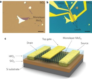
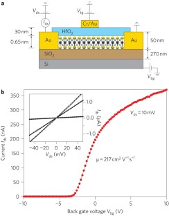
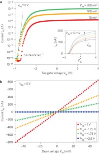
Two-dimensional materials are attractive for use in next-generation nanoelectronic devices because, compared to one-dimensional materials, it is relatively easy to fabricate complex structures from them. The most widely studied two-dimensional material is graphene1,2, both because of its rich physics3,4,5 and its high mobility6. However, pristine graphene does not have a bandgap, a property that is essential for many applications, including transistors7. Engineering a graphene bandgap increases fabrication complexity and either reduces mobilities to the level of strained silicon films8,9,10,11,12,13 or requires high voltages14,15. Although single layers of MoS2 have a large intrinsic bandgap of 1.8 eV (ref. 16), previously reported mobilities in the 0.5–3 cm2 V−1 s−1 range17 are too low for practical devices. Here, we use a halfnium oxide gate dielectric to demonstrate a room-temperature single-layer MoS2 mobility of at least 200 cm2 V−1 s−1, similar to that of graphene nanoribbons, and demonstrate transistors with room-temperature current on/off ratios of 1 × 10⁸ and ultralow standby power dissipation. Because monolayer MoS2 has a direct bandgap16,18, it can be used to construct interband tunnel FETs19, which offer lower power consumption than classical transistors. Monolayer MoS2 could also complement graphene in applications that require thin transparent semiconductors, such as optoelectronics and energy harvesting.
This is a preview of subscription content, access via your institution
Access options
Subscribe to this journal
Receive 12 print issues and online access
$259.00 per year
only $21.58 per issue
Buy this article
- Purchase on Springer Link
- Instant access to full article PDF
Prices may be subject to local taxes which are calculated during checkout
Change history
17 February 2011
In the version of this Letter originally published online, the label 'Vtg' was missing from Fig. 3a and the expression 'μ = 217 cm-2 Vs' should have read 'μ = 217 cm2 V-1 s-1' in Fig. 3b. These errors have now been corrected in all versions of the Letter.
References
Novoselov, K. S. et al. Electric field effect in atomically thin carbon films. Science 306, 666–669 (2004).
Berger, C. et al. Ultrathin epitaxial graphite: 2D electron gas properties and a route toward graphene-based nanoelectronics. J. Phys. Chem. B 108, 19912–19916 (2004).
Novoselov, K. S. et al. Two-dimensional gas of massless Dirac fermions in graphene. Nature 438, 197–200 (2005).
Zhang, Y., Tan, Y.-W., Stormer, H. L. & Kim, P. Experimental observation of the quantum Hall effect and Berry's phase in graphene. Nature 438, 201–204 (2005).
Du, X., Skachko, I., Duerr, F., Luican, A. & Andrei, E. Y. Fractional quantum Hall effect and insulating phase of Dirac electrons in graphene. Nature 462, 192–195 (2009).
Bolotin, K. I. et al. Ultrahigh electron mobility in suspended graphene. Solid State Commun. 146, 351–355 (2008).
The International Technology Roadmap for Semiconductors. http://www.itrs.net/Links/2009ITRS/Home2009.htm (2009).
Han, M. Y., Ozyilmaz, B., Zhang, Y. & Kim, P. Energy band-gap engineering of graphene nanoribbons. Phys. Rev. Lett. 98, 206805 (2007).
Li, X., Wang, X., Zhang, L., Lee, S. & Dai, H. Chemically derived, ultrasmooth graphene nanoribbon semiconductors. Science 319, 1229–1232 (2008).
Jiao, L., Zhang, L., Wang, X., Diankov, G. & Dai, H. Narrow graphene nanoribbons from carbon nanotubes. Nature 458, 877–880 (2009).
Sols, F., Guinea, F. & Neto, A. H. C. Coulomb blockade in graphene nanoribbons. Phys. Rev. Lett. 99, 166803 (2007).
Yoon, Y. & Guo, J. Effect of edge roughness in graphene nanoribbon transistors. Appl. Phys. Lett. 91, 073103 (2007).
Obradovic, B. et al. Analysis of graphene nanoribbons as a channel material for field-effect transistors. Appl. Phys. Lett. 88, 142102 (2006).
Zhang, Y. et al. Direct observation of a widely tunable bandgap in bilayer graphene. Nature 459, 820–823 (2009).
Xia, F., Farmer, D. B., Lin, Y.-M. & Avouris, P. Graphene field-effect transistors with high on/off current ratio and large transport band gap at room temperature. Nano Lett. 10, 715–718 (2010).
Mak, K. F., Lee, C., Hone, J., Shan, J. & Heinz, T. F. Atomically thin MoS2: a new direct-gap semiconductor. Phys. Rev. Lett. 105, 136805 (2010).
Novoselov, K. S. et al. Two-dimensional atomic crystals. Proc. Natl Acad. Sci. USA 102, 10451–10453 (2005).
Splendiani, A. et al. Emerging photoluminescence in monolayer MoS2 . Nano Lett. 10, 1271–1275 (2010).
Banerjee, S., Richardson, W., Coleman, J. & Chatterjee, A. A new three-terminal tunnel device. Electron Dev. Lett. 8, 347–349 (1987).
Frindt, R. F. Single crystals of MoS2 several molecular layers thick. J. Appl. Phys. 37, 1928–1929 (1966).
Joensen, P., Frindt, R. F. & Morrison, S. R. Single-layer MoS2 . Mater. Res. Bull. 21, 457–461 (1986).
Schumacher, A., Scandella, L., Kruse, N. & Prins, R. Single-layer MoS2 on mica: studies by means of scanning force microscopy. Surf. Sci. Lett. 289, L595–L598 (1993).
Kam, K. K. & Parkinson, B. A. Detailed photocurrent spectroscopy of the semiconducting group VIB transition metal dichalcogenides. J. Phys. Chem. 86, 463–467 (1982).
Feldman, Y., Wasserman, E., Srolovitz, D. J. & Tenne, R. High-rate, gas-phase growth of MoS2 nested inorganic fullerenes and nanotubes. Science 267, 222–225 (1995).
Remskar, M. et al. Self-assembly of subnanometer-diameter single-wall MoS2 nanotubes. Science 292, 479–481 (2001).
Schwierz, F. Graphene transistors. Nature Nanotech. 5, 487–496 (2010).
Benameur, M., Radisavljevic, B., Sahoo, S., Berger, H. & Kis, A. Visibility of dichalcogenide nanolayers. http://lanl.arxiv.org/abs/1006.1048v1 (2010).
Ishigami, M., Chen, J. H., Cullen, W. G., Fuhrer, M. S. & Williams, E. D. Atomic structure of graphene on SiO2 . Nano Lett. 7, 1643–1648 (2007).
Ayari, A., Cobas, E., Ogundadegbe, O. & Fuhrer, M. S. Realization and electrical characterization of ultrathin crystals of layered transition-metal dichalcogenides. J. App. Phys. 101, 014507 (2007).
Fivaz, R. & Mooser, E. Mobility of charge carriers in semiconducting layer structures. Phys. Rev. 163, 743–755 (1967).
Debdeep, J. & Aniruddha, K. Enhancement of carrier mobility in semiconductor nanostructures by dielectric engineering. Phys. Rev. Lett. 98, 136805 (2007).
Chen, F., Xia, J., Ferry, D. K. & Tao, N. Dielectric screening enhanced performance in graphene FET. Nano Lett. 9, 2571–2574 (2009).
Bohr, M. T., Chau, R. S., Ghani, T. & Mistry, K. The high-k solution. IEEE Spectrum 44, 29–35 (2007).
Mistry, K. et al. A 45 nm logic technology with high-k + metal gate transistors, strained silicon, 9 Cu interconnect layers, 193 nm dry patterning, and 100% Pb-free packaging. IEEE Tech. Dig. IEDM 247–250 (2007).
Lemme, M. C., Echtermeyer, T. J., Baus, M. & Kurz, H. A graphene field-effect device. IEEE Electron Dev. Lett. 28, 282–284 (2007).
Fonoberov, V. A. & Balandin, A. A. Giant enhancement of the carrier mobility in silicon nanowires with diamond coating. Nano Lett. 6, 2442–2446 (2006).
Gomez, L., Aberg, I. & Hoyt, J. L. Electron transport in strained-silicon directly on insulator ultrathin-body n-MOSFETs with body thickness ranging from 2 to 25 nm. IEEE Electron Dev. Lett. 28, 285–287 (2007).
Duan, X. et al. High-performance thin-film transistors using semiconductor nanowires and nanoribbons. Nature 425, 274–278 (2003).
Liao, L. et al. High-speed graphene transistors with a self-aligned nanowire gate. Nature 467, 305–308 (2010).
Dean, C. R. et al. Boron nitride substrates for high-quality graphene electronics. Nature Nanotech. 5, 722–726 (2010).
Acknowledgements
The authors thank G. Seifert, T. Heine and Y. Paiss for useful discussions. Device fabrication was carried out in part in the EPFL Center for Micro/Nanotechnology (CMI). Thanks go to K. Lister (CMI) for technical support with electron-beam lithography. This work was financially supported by the European Research Council (grant no. 240076, FLATRONICS: electronic devices based on nanolayers).
Author information
Authors and Affiliations
Contributions
B.R., J.B., V.G. and A.K. worked on device fabrication and contact optimization. A.R. built the system for atomic layer deposition of HfO2. B.R. and A.K. performed measurements and analysed the data presented in the paper and Supplementary Information. A.K. initiated the research and wrote the manuscript. All the authors read and commented on the manuscript.
Corresponding author
Ethics declarations
Competing interests
The authors declare no competing financial interests.
Supplementary information
Rights and permissions
About this article
Cite this article
Radisavljevic, B., Radenovic, A., Brivio, J. et al. Single-layer MoS2 transistors. Nature Nanotech 6, 147–150 (2011). https://doi.org/10.1038/nnano.2010.279
Received:
Accepted:
Published:
Issue Date:
DOI: https://doi.org/10.1038/nnano.2010.279
This article is cited by
-
Advance in additive manufacturing of 2D materials at the atomic and close-to-atomic scale
npj 2D Materials and Applications (2024)
-
Critical assessment of G0W0 calculations for 2D materials: the example of monolayer MoS2
npj Computational Materials (2024)
-
Hard ferromagnetism in van der Waals Fe3GaTe2 nanoflake down to monolayer
npj 2D Materials and Applications (2024)
-
Broadband miniaturized spectrometers with a van der Waals tunnel diode
Nature Communications (2024)
-
Ultrashort vertical-channel MoS2 transistor using a self-aligned contact
Nature Communications (2024)

