Abstract
Optical techniques have advanced considerably in recent years to enable processing of surfaces with a resolution less than the wavelength of light. Despite the highly selective nature of light-matter interactions, however, efforts to increase resolution to the scale of single atoms are hampered by rapid and efficient dissipation of the absorbed energy to the surrounding matrix. Here we show that two-photon surface excitation using ultraviolet light provides a method for selectively removing carbon from diamond surfaces. Polished surfaces etched by this method develop ultra-deep subwavelength structures with morphologies dependent on the polarization of the incident laser with respect to the crystal axes. As well as revealing a practical and versatile method for nano-patterning of diamond surfaces, we show that the results comprise mesoscopic evidence for bond scission via a highly localized optical interaction that may lead to the development of new optical approaches for ultra-nanoscale (<10 nm) surface structuring.
Introduction
Manipulation of single or groups of atoms on surfaces has enormous potential for the development of future nano-scale devices. Currently, the most powerful examples of atom-scale manipulation involve the use of forces and currents at the apex of sharp tips in scanning probe microscopy1,2. However, these techniques are often unsuited to the strongly bound and electrically insulating nature of many covalently bonded materials. In contrast, strong covalent bonds offer the advantage that the associated bonding electrons comprise highly localized oscillators that can be targeted resonantly using light. Single bonds between carbon atoms, for example, carry electronic absorption signatures that are relatively unperturbed by the neighbouring bonding environment3,4. Therefore, light, with all its practical conveniences, has the potential to extend resolution below the subwavelength scales already seen5,6,7 and to enable targeted bond breakage and atom manipulation for materials incompatible with current scanning probe methods.
To date, only bonds in gas phase species or between H adsorbates on Si surfaces have exhibited photo-selective bond scission8,9,10. We have investigated single-crystal diamond as a promising candidate for revealing photo-selective scission of structural bonds in a strong covalently bound system. In this respect, diamond is ideal. It presents a simple symmetrical structure of sp3-bonded carbon atoms while being also a material of enormous interest in science and technology11,12,13,14,15,16,17. Furthermore, diamond exhibits an unusual mode of carbon removal from the surface when excited by photons of energy approaching the bandgap. It has been shown that carbon atoms are ejected from the surface when using wavelengths near 250 nm (refs 18, 19) at a rate consistent with a two-photon excitation mechanism18 and a cross-section of approximately 20 Goeppert-Mayers. The two-photon dependence, along with a lack of threshold, is indicative of a material ejection mechanism intrinsically different from usual laser ablation and desorption which rely upon thermal- or plasma-mediated ejection mechanisms. The process is also distinguished from laser ablation of diamond by the absence of graphite formation on the treated surface18,19.
Here we show that the two-photon-induced ejection mechanism in diamond involves light coupling with localized states that preserve the light polarization information. We find that the ejection probability displays a strong dependence on the light polarization with respect to the lattice bond directions. By repetitive pulsed exposure of the surface, these properties are revealed as deep-subwavelength patterns etched into the surface that exhibit striking variations in morphology as the polarization is rotated with respect to crystal axes.
Results
Patterning of {100} and {110} surfaces
Diamond single crystals were exposed to 266 nm laser pulses at fluences approximately half of the ablation threshold. By etching to depths of several hundred nanometers, patterns were clearly resolved by electron microscopy. For a diamond cubic face with light at normal incidence, the nano-pattern polarization dependence can be effectively characterized by considering three crystal directions of high symmetry as shown in Fig. 1. When the polarization is parallel to [110] (E||[110]), the pattern consists of faceted ridges oriented perpendicular to the polarization (Fig. 1b). The ridges are quasi-regular with a spatial frequency in the range 0.3–4 λp−1, where λp=266 nm is the laser wavelength. More complex patterns are obtained when using polarization away from the [110] direction. For E||[210] (Fig. 1c), the average ridge direction is approximately 4.5 degrees from the [110] direction and no longer perpendicular to the laser polarization. The ridges are narrower, exhibit more bifurcations and contain spatial frequencies extending up to 5 λp−1. When aligned along the cubic direction E||[100] (Fig. 1d), the pattern consists of a cross hatched or grid-like structure oriented within a few degrees of [110]. Spatial frequencies up to 4–5 λp−1 appear in the vertical and horizontal directions. Feature sizes as short as 50 nm are clearly observed in the magnified inset image. The contrast in the spatial frequency content for each image is clearly visible in the two-dimensional power spectra shown in Fig. 2. Upon rotation of the writing beam polarization by angles beyond [100], the pattern reverts progressively to resemble again those identified for E||[210] and [110], except reflected about the [100] axis in accordance with the C4 rotational symmetry of the lattice surface.
(a) Polarization and lattice bond directions as viewed in the direction of the incident laser beam. (b–d) 6.0 × 4.5 μm Images for a laser beam at normal incidence with polarizations parallel to [110], [210] and [100]. Scale bars, 1,000 nm, except for inset of (d), 100 nm. In each case the laser dose was 10.3 MJ cm−2, and the average depth of material removed was 550 nm. The inset image contains a close-up view (0.97 × 0.65 μm) of the pattern in d.
The raw images (a–c) are reproduced in the top-row for ease of comparison. Corresponding power spectra (d–f) and auto-correlations (g–i) for the (001) surface images of Fig. 1. Frequencies are expressed in reciprocal laser wavelengths. Scale bars, 1 μm.
The contrasting symmetry and distribution of local environments for atoms on a {110} surface are also evident in the etched patterns. Three pattern types distinct from those for the {100} face were obtained for polarizations parallel to the low Miller index directions [001], [111] and [110] (Fig. 3). For E||[001], faceted ridges of spatial frequency approximately 1.6 λp−1 were formed with direction perpendicular to the polarization. In contrast to the ridges observed on the {100} face, these faceted ridges exhibit stepped dislocations along each ridge spaced by about 1 μm. For E||[111], parallel running ridges are also observed but have a complex unfaceted cross-sectional shape and a direction approximately 45° from [001] and 80° from the laser polarization direction. The pattern for E||[110] consists of a ripple pattern of similar spatial frequency (Fig. 4), but in this case the ripples are more sinusoidal and once again aligned perpendicular to the laser polarization.
(a) Polarization and lattice bond directions as viewed in the direction of the incident laser beam. (b–d) 3.0 × 2.25 μm images for laser polarizations parallel to [001], [111] and [110] directions. Scale bars, 500 nm. The laser dose was 10.8 MJ cm−2 in each case. The etch depths were 350 nm, 510 nm and 530 nm, respectively.
The raw images (a–c) are reproduced in the top-row for ease of comparison. Corresponding power spectra (d–f) and auto-correlations (g–i) for the surface images of Fig. 3. Frequencies are expressed in reciprocal laser wavelengths. Scale bars, 500 nm.
The patterns of Figs 1 and 3 are representative of the polarization dependence observed for the hundreds of etches we carried out on several diamond substrates with nitrogen content in the range 20–100 p.p.b. Polarizations along 〈1yz〉 crystal directions where y, z=0 or 1 produce the simplest patterns–that is, those easily identifiable as ridges, ripples or grids. These patterns often exhibit good long-range order (See Figs 2g–i and 4g–i). We noted that facetted ridges are generally obtained when the laser polarization is parallel to projections of 〈111〉 on the surface plane. Scanning probe microscopy indicates that the facet angles are often consistent with {111} and {221} surfaces as shown, for example, for a {100} surface etched with E||〈110〉 (Fig. 5).
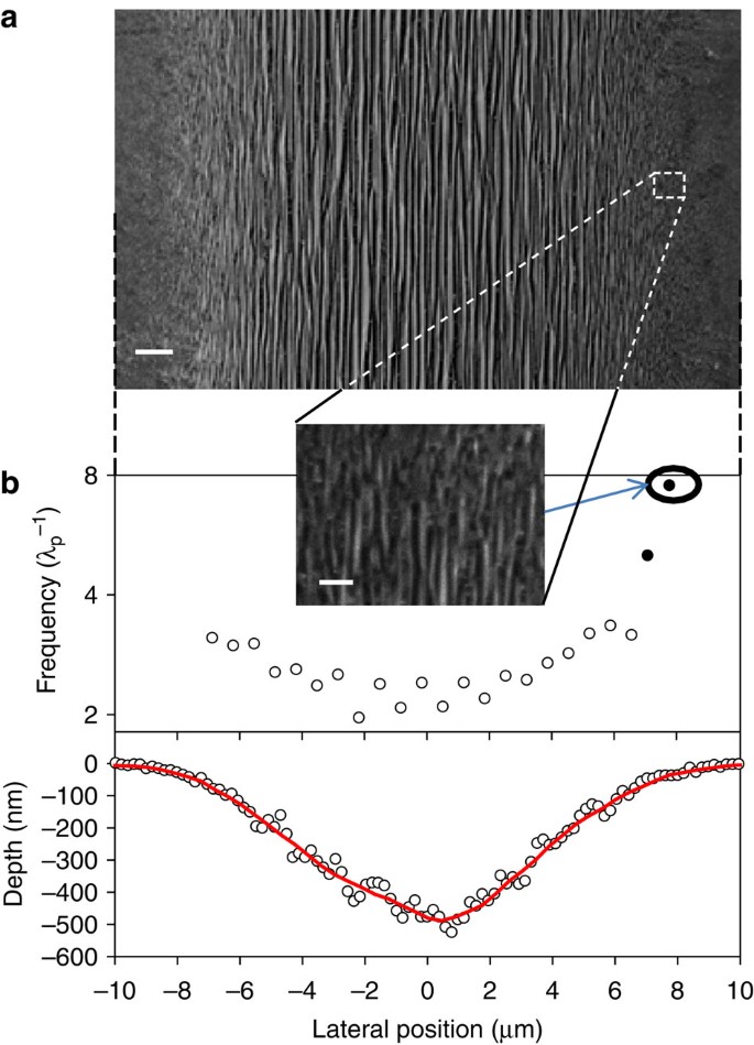
(a) 17.2 × 12.9 μm SEM image of a trench etched for E||〈110〉 showing the decrease in spatial frequency with etch depth. The trench was created using a rastered beam in the vertical direction 30 passes spaced by 2 μm. Periodic structures spaced by 20 nm are observed at the trench fringe as shown in the inset image. Scale bar, 1,000 nm, inset image, 100 nm. (b) Frequency expectation value of the 1-D power spectrum as a function of lateral position (top) and etch depth (bottom). For positions more than 6.5 μm from the trench axis, frequencies were obtained using higher magnification images (solid symbols).
Factors influencing morphology and frequency
Pattern development is a function of depth and depends only weakly on laser fluence in the investigated range of 2–50 J cm−2. For small etch depths, the patterns exhibit random structure of high spatial frequency, that progress to clear regular structures of lower frequency with further removal of material (Fig. 6). With the field emission electron microscope, we were able to resolve feature sizes as small as 10–20 nm as shown in the inset image of Fig. 6a. The increase in spatial frequency at the fringes of the pattern suggests that much smaller features are created for very small etch depths. Pattern evolution was observed to proceed in the same way across all parts of the beam cross-section. We rule out beam back reflection from the second surface of the sample as a major influence on pattern development; the observed decrease in pattern spatial frequency on etch depth is inconsistent with an interferometric mechanism. Furthermore, identical patterns were reproduced on sample thicknesses from 1.5 to 22 Rayleigh ranges, for which the retro-reflected intensities of the incident beam decrease from 5.5 to 0.03%. No change in pattern was visible when varying angle of incidence by up to 5°.
(a) 3-D and (b) 2-D AFM images of a 1.3 × 1.3 μm area in an etched pattern with E||110] (as in Fig. 1b). (c) The image cross-section for the horizontal line shown in (b). The solid lines indicate portions of the cross-section that fall closely within {111} (blue) and {221} (red) planes.
Discussion
The observed patterning has starkly contrasting properties to the laser-induced periodic surface structuring observed, to date, in any material20,21,22,23,24,25,26,27 including diamond20,28,29,30,31. For incident intensities near the ablation threshold or at the fringes of an ablation spot, ripple-like structures are produced with periodicity approximately equal to the wavelength of the incident light and with direction perpendicular to the laser polarization, except in a few special cases that combine angle of incidence and polarization to perturb the pattern symmetry25,27. For studies on single-crystal substrates20,21,27,28,29,30, no lattice-polarization angle dependence was observed. To date, ripple formation has been explained in terms of interference effects between the light beam and the light-induced waves established on the heated surface32,33.
In our case, the pattern morphologies are much more diverse according to the crystal orientation and much higher spatial frequencies are obtained. The influence of crystal orientation is most evident on the cubic face where the periodic structures show a closer relationship with the bond directions (Fig. 1b–d) than to the laser polarization. For the special case of E||[100], where the polarization has an equal projection along all bonds, the grid pattern is aligned to surface projections of carbon-carbon lattice bonds and the pattern shares the C4 point symmetry of the surface (Fig. 1d). We found that the same grid structure and orientation were reproduced using circular polarization, which likewise projects an equal polarization along all lattice bonds. The pattern type and orientation is thus principally determined by the overlap between the polarization and directional surface states, rather than collective surface wave excitations of previous laser-induced patterns20,21,22,23,24,25,26,27,28,29,30,31,32,33. Our observations of structures with period less than 20 nm for small etch depths are consistent with a highly localized light-material interaction.
We propose that the patterns develop as a result of anisotropic coupling of photons with surface bonds in convolution with a probability for carbon ejection dependent on the local bonding environment. As carbon removal progresses, the spatially dependent ejection probability becomes visible on the mesoscale in the form of patterns containing symmetries of the lattice surface. The rich variety of patterns produced as functions of facet and polarization reveal that the ejection probability is a complex function of the local surface structure and beam polarization. Such an ejection mechanism is consistent with the thresholdless and ‘cold’ nature of the process, and is distinct from the exponential and thermal nature of the periodic structuring observed previously20,21,22,23,24,25,26,27,28,29,30,31,32,33,34,35 when using higher intensities, either near or above the ablation threshold. Further work is needed to determine whether bond scission results from direct coupling of the ultraviolet with carbon–carbon bonds or is reliant on cooperative processes with electronic states associated with surface reconstructions, radical sites or chemisorbed atoms. For example, the two-photon excitation may occur via gap-state resonances34 associated with these surface configurations.
The polarization-dependent ejection probability demonstrated here is a novel phenomenon with implications in photochemistry, surface physics and laser surface structuring. As the process can be performed in ambient conditions, it provides a straightforward and area-scalable method for tailoring the nano-scale morphology of diamond surfaces. This may be of direct interest in areas such as ultralow friction surfaces15, biochemical substrates14, and surface-enhanced ultrasensitive molecular sensors35. Of more fundamental importance, the evidence for coupling between the light field and localized bonds reveals promise for developing optical tools for bond-specific manipulation in covalent materials. Such manipulation on dimensions approaching the atomic scale may be made possible in future using, for example, tip-enhanced nano-optical techniques36,37. This may provide a pathway forward for engineering diamond devices that benefit from increased resolution such as low-loss waveguides38, quantum devices11,12,13,39, high-speed electronics40 and high-density data storage41.
Methods
Sample etching
The single-crystal samples were Type IIa diamond of rms roughness 1 nm (Optical Grade, Element 6) and cleaned using a piranha chemical solution before UV exposure. The UV beam from a 266 nm laser of pulse duration 11 ns full-width-half maximum and repetition rate 13-14 kHz was focused to a waist radius of 4.8 μm on the sample top surface using a 25 mm focal length objective. The fluence was selected to be approximately 50% below the ablation threshold of 100 J cm−2, which provided etch rates of approximately 10 nm per second without risk of ablation. The ablation threshold is defined here as the fluence at which there is a 50% probability for explosive material removal for a burst of 103 pulses. The two-photon cross-section of 20 GM was evaluated using the measured18 etch rate of 3 pm per pulse from the {100} surface for a beam with a pulse fluence of 60 J cm−2, spot-size 4.8 μm and pulse duration 11 ns. For this calculation, the carbon atom surface density was taken as twice the unit cell surface density. The sample was accurately positioned and rastered using a computer-controlled positioning stage. The polarization was aligned by rotation of the sample on the stage against facet orientation specified by the manufacturer and confirmed by us using polarized Raman spectroscopy.
Surface analysis
Etch depths were measured using an optical profiler (VEECO, Wyko NT3300, 514 nm, Objective NA=0.85). Pattern images were obtained using a field-emission SEM (JEOL JSM-7800 F). The SEM electron voltage was 2 kV, which we found provided the best resolution and minimal image distortion of the UV-treated diamond surface. Pattern profiles were obtained by atomic force microscopy (MT-NDT Ntegra Spectra) in non-contact mode using a Si tip of radius of curvature 10 nm (NT-MDT NSG01). Image analysis software (Image Analysis 3, NT-MDT) was used to reduce the effects of the finite tip radius.
Additional information
How to cite this article: Lehmann, A. et al. Two-photon polarization-selective etching of emergent nano-structures on diamond surfaces. Nat. Commun. 5:3341 doi: 10.1038/ncomms4341 (2014).
References
Eigler, D. & Schweizer, E. Positioning single atoms with a scanning tunnelling microscope. Nature 344, 524–526 (1990).
Custance, O., Perez, R. & Morita, S. Atomic force microscopy as a tool for atom manipulation. Nat. Nanotech. 4, 803–810 (2009).
Raymonda, J. W. & Simpson, W. Experimental and theoretical study of sigma‐bond electronic transitions in alkanes. J. Chem. Phys. 47, 430–448 (1967).
Robertson, J. Diamond-like amorphous carbon. Mater. Sci. Eng. R-Rep. 37, 129–281 (2002).
Kawata, S., Sun, H. B., Tanaka, T. & Takada, K. Finer features for functional microdevices. Nature 412, 697–698 (2001).
Joglekar, A. P., Liu, H.-H., Meyhöfer, E., Mourou, G. & Hunt, A. J. Optics at critical intensity: applications to nanomorphing. Proc. Natl Acad. Sci. USA 101, 5856–5861 (2004).
Andrew, T. L., Tsai, H.-Y. & Menon, R. Confining light to deep subwavelength dimensions to enable optical nanopatterning. Science 324, 917–921 (2009).
Levis, R. J., Menkir, G. M. & Rabitz, H. Selective bond dissociation and rearrangement with optimally tailored, strong-field laser pulses. Science 292, 709–713 (2001).
Vondrak, T. & Zhu, X.-Y. Direct photodesorption of atomic hydrogen from Si(100) at 157 nm: experiment and simulation. J. Phy. Chem. B 103, 4892–4899 (1999).
Vondrak, T. & Zhu, X.-Y. Dissociation of a surface bond by direct optical excitation: H-Si(100). Phys. Rev. Lett. 82, 1967–1970 (1999).
Burek, M. J. et al. Free-standing mechanical and photonic nanostructures in single-crystal diamond. Nano. Lett. 12, 6084–6089 (2012).
Prawer, S. & Greentree, A. Diamond for quantum computing. Science 320, 1601–1602 (2008).
Maze, J. R. et al. Nanoscale magnetic sensing with an individual electronic spin in diamond. Nature 455, 644–647 (2008).
Yang, W., Auciello, O., Butler, J. & Cai, W. DNA-modified nanocrystalline diamond thin-films as stable, biologically active substrates. Nat. Mat. 1, 253–258 (2002).
Heimberg, J. A., Wahl, K. J., Singer, I. L. & Erdemir, A. Superlow friction behavior of diamond-like carbon coatings: time and speed effects. Appl. Phys. Lett. 78, 2449–2451 (2001).
Mildren R. P., Rabeau J. R. (eds)Optical Engineering of Diamond Wiley-VCH: Berlin, Germany, (2013).
Ristein, J. Surface science of diamond: familiar and amazing. Surf. Sci. 600, 3677–3689 (2006).
Mildren, R. P. et al. Characteristics of 2-photon ultraviolet laser etching of diamond. Opt. Mat. Express 1, 576–585 (2011).
Kononenko, V. V., Komlenok, M. S., Pimenov, S. M. & Konov, V. I. Photoinduced laser etching of a diamond surface. Quantum Electron 37, 1043–1046 (2007).
Huang, M., Zhao, F., Cheng, Y., Xu, N. & Xu, Z. Origin of laser-induced near-subwavelength ripples: interference between surface plasmons and incident laser. ACS Nano 3, 4062–4070 (2009).
Huang, M., Zhao, F., Cheng, Y., Xu, N. & Xu, Z. The morphological and optical characteristics of micro/nanostructures on GaAs, Si, and brass. Opt. Express 18, 5694–5696 (2010).
Wang, C., Huo, H., Johnson, M., Shen, M. & Mazur, E. The thresholds of surface nano-/micro-morphology modifications with femtosecond laser pulse irradiations. Nanotechnology 21, 75304 (2010).
Liu, Y., Jiang, M. Q., Yang, G. W., Guan, Y. J. & Dai, L. H. Surface rippling on bulk metallic glass under nanosecond pulse laser ablation. Appl. Phys. Lett. 99, 191902 (2011).
Tomita, T., Fukumori, Y., Kinoshita, K., Matsuo, S. & Hashimoto, S. Observation of laser-induced surface waves on flat silicon surface. Appl. Phys. Lett. 92, 013104 (2008).
Young, J., Preston, J., Driel Van, H. & Sipe, J. Laser-induced periodic surface structure. II. Experiments on Ge, Si, Al, and brass. Phys. Rev. B 27, 1155–1172 (1983).
Young, J., Sipe, J. & Driel, H. Van Laser-induced periodic surface structure. III. Fluence regimes, the role of feedback, and details of the induced topography in germanium. Phys. Rev. B 30, 2001–2015 (1984).
Reif, J., Costache, F., Henyk, M. & Pandelov, S. V. Ripples revisited: non-classical morphology at the bottom of femtosecond laser ablation craters in transparent dielectrics. Appl. Surf. Sci. 197-198, 891–895 (2002).
Shinoda, M., Gattass, R. R. & Mazur, E. Femtosecond laser-induced formation of nanometer-width grooves on synthetic single-crystal diamond surfaces. J. Appl. Phys. 105, 053102 (2009).
Hsu, E. M., Mailman, N. A., Botton, G. A. & Haugen, H. K. Microscopic investigation of single-crystal diamond following ultrafast laser irradiation. Appl. Phys. A 103, 185–192 (2010).
Ozkan, A. M. et al. Femtosecond laser-induced periodic structure writing on diamond crystals and microclusters. Appl. Phys. Lett. 75, 3716–3718 (1999).
Huang, M., Zhao, F., Cheng, Y., Xu, N. & Xu, Z. Mechanisms of ultrafast laser-induced deep-subwavelength gratings on graphite and diamond. Phys. Rev. B 79, 125436 (2009).
Sipe, J., Young, J., Preston, J. & Driel, H. Van. Laser-induced periodic surface structure. I. Theory. Phys. Rev. B 27, 1141–1154 (1983).
Bhardwaj, V. et al. Optically produced arrays of planar nanostructures inside fused silica. Phys. Rev. Lett. 96, 057404 (2006).
Loh, K. et al. Surface oxygenation studies on (100)-oriented diamond using an atom beam source and local anodic oxidation. Surf. Sci. 505, 93–114 (2002).
Buividas, R. et al. Mechanism of fine ripple formation on surfaces of (semi)transparent materials via a half-wavelength cavity feedback. Nanotechnology 22, 055304 (2011).
Leggett, G. J. Scanning near-field photolithography-surface photochemistry with nanoscale spatial resolution. Chem. Soc. Rev. 35, 1150–1161 (2006).
Wu, S. W., Ogawa, N. & Ho, W. Atomic-scale coupling of photons to single-molecule junctions. Science 312, 1362–1365 (2006).
Tomljenovic-Hanic, S. et al. inOptical Engineering of Diamond 311–351Wiley-VCH: Weinheim, (2013).
Priolo, F., Gregorkiewicz, T., Galli, M. & Krauss, T. F. Silicon nanostructures for photonics and photovoltaics. Nat. Nanotech. 9, 19–32 (2014).
Moran, D. A., Fox, O. J., McLelland, H., Russell, S. & May, P. W. Scaling of hydrogen-terminated diamond FETs to sub-100-nm gate dimensions. Electron Device Lett., IEEE 32, 599–601 (2011).
Mamin, H. J., Ried, R. P., Terris, B. D. & Rugar, D. High-density data storage based on the atomic force microscope. Proc. IEEE 87, 1014–1027 (1999).
Acknowledgements
This material is based on research sponsored by the Australian Research Council Future Fellowship Scheme (FT0990622) and Discovery Grant (DP130103799), and the US Air Force Research Laboratory Grant under agreement number FA2386-12-1-4055. We are grateful for the assistance of Benjamin Johnston and Peter Ha of the OptoFab, Node of the Australian National Fabrication Facility, Debra Birch of the Science Faculty Microscopy Unit, and Adam Joyce for his expertise in optical profilometry.
Author information
Authors and Affiliations
Contributions
A.L. and R.P.M. performed the etching. C.B. performed the atomic force microscopy. R.P.M. designed the experiments. R.P.M. wrote the manuscript. All authors participated in data analysis and manuscript preparation.
Corresponding author
Ethics declarations
Competing interests
The authors declare no competing financial interests.
Rights and permissions
About this article
Cite this article
Lehmann, A., Bradac, C. & Mildren, R. Two-photon polarization-selective etching of emergent nano-structures on diamond surfaces. Nat Commun 5, 3341 (2014). https://doi.org/10.1038/ncomms4341
Received:
Accepted:
Published:
DOI: https://doi.org/10.1038/ncomms4341
This article is cited by
-
Correlation between surface etching and NV centre generation in laser-irradiated diamond
Applied Physics A (2018)
-
Study of textured ZnS irradiated by femtosecond laser pulses
Optical and Quantum Electronics (2016)
Comments
By submitting a comment you agree to abide by our Terms and Community Guidelines. If you find something abusive or that does not comply with our terms or guidelines please flag it as inappropriate.


