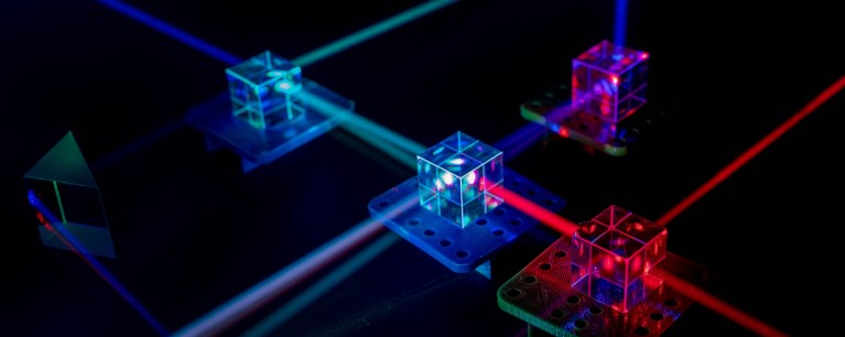
Light-based quantum computers have several advantages over those based on semiconductors.© luchschenF/Shutterstock
A ‘squeezed’ light source capable of generating qubits — the quantum equivalent of bits — represents a breakthrough in the race to create practical quantum computers based on light. The advance was announced by the Japanese telecommunications company NTT, in partnership with the University of Tokyo, in December 2021.
Quantum computers are the future of computing since they vastly outperform conventional computers for certain types of problems. But whereas a typical laptop computer might have tens or hundreds of billions of bits in its RAM, most quantum computers today are limited to only a handful of qubits, because they need ultracold superconductors to protect electronic spin states from outside influences. In contrast, the NTT light-based technology runs at room temperature and can be coupled to an optical fibre, potentially enabling a single laser to generate hundreds of qubits.
“Optical-based approaches to quantum computing have the huge advantage of being scalable,” explains Takeshi Umeki, a distinguished researcher at NTT Device Technology Laboratories. “This makes a big difference in producing quantum computers with fault-tolerant hardware.”
The secret to NTT’s squeezed-light source lies in a special type of crystal known as periodically poled lithium niobate (PPLN). It can convert incoming laser light to different colours, allowing access to parts of the electromagnetic spectrum that conventional lasers cannot reach, thus extending lasers’ range of applications.
Cutting-edge change
When he joined NTT in the 1990s, Yoshiki Nishida worked on PPLN waveguides — devices that enable wavelength conversion with minimal energy loss. With a background in materials science, Nishida was tasked with improving the performance of all-optical wavelength converters for telecommunication applications.

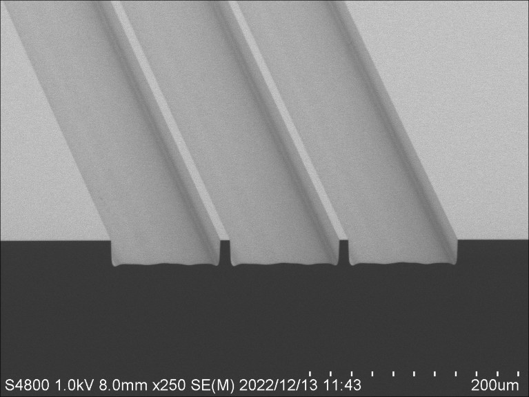
Electron microscopy image showing the cross section of a waveguide based on PPLN.© NTT Electronics Corporation
But demand for such wavelength converters plummeted when the IT ‘dot-com’ bubble burst in 2001. To change course, NTT decided to target non-traditional markets such as the biomedical sector, which at the time lacked reliable yellow-light lasers to image compounds such as fluorescent proteins.
One of the most interesting aspects of NTT’s waveguides is that “we can make any colour by choosing the wavelength of the incoming pump laser,” notes Nishida, who is now assistant manager of the Photonics Component Business Group at NTT Electronics. This ability allows researchers and engineers to tune the laser wavelength for specific applications.
PPLN waveguides can perform this feat thanks to fabrication techniques that create patterns of points on lithium niobate wafers where the crystal’s electric dipole alternately points up or down. This layout is ideal for things such as producing an output photon of a different colour by combining two input photons from a high-intensity laser.

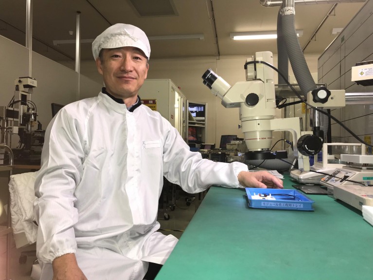
Yoshiki Nishida and his team have greatly boosted the efficiency of PPLN crystals, making them useful for practical applications.© NTT Electronics Corporation
Although the researchers could calculate the two-colour input needed to generate yellow-light lasers, typical, bulk-scale PPLN crystals could not yield enough output light for practical applications. “The idea existed, but we needed a way to boost its efficiency by more than 1,000 times,” recalls Nishida.
The solution to the efficiency problem came at the end of a razor-sharp saw. After direct bonding a PPLN wafer to a substrate, the team mechanically cut narrow ridges into the wafer using diamond blades. These ridges focus the input light to a very small area, which makes nonlinear interactions more favourable.
The mechanically cut waveguides, which Nishida says surprised academics when the concept was first announced, featured low propagation losses because of their polished surfaces. Another bonus was a circular output mode pattern that enabled the light to be easily coupled to optical fibres.
Gain of function
“There were no prior studies on cutting waveguides at the time. We did it because the etching and chemical vapour deposition technology was just not there,” says Nishida. “Customers became interested in the approach when they saw the capabilities. It’s highly compact and robust because, unlike a typical laser, it doesn’t need a special cavity structure.”
After NTT demonstrated yellow laser light in 2004, manufacturers of laser confocal microscopes quickly adopted this technology. In addition, Nishida and his project team received an internal NTT award for the creation of new business in non-telecom markets.
When researchers began to appreciate the power of PPLN waveguides to manipulate and confine light, they applied the technology in projects such as ultraprecise optical clocks and laser cooling techniques to take atoms to near absolute zero. One such scientist was Umeki, who joined NTT in 2004 in the hope of developing realistic PPLN devices.
First assigned to optimize a new technique for fabricating PPLN ridges using plasma etching instead of saws, Umeki soon turned his talents towards telecommunication applications of PPLN technology. These included amplification techniques that reduce noise in long-haul systems, and parametric nonlinear processes where a single input photon is split into two new photons, with colour wavelengths restricted only by energy-conservation principles.
“Parametric devices are really helpful for users,” notes Umeki. “You can inject a laser beam by just connecting an optical fibre.”

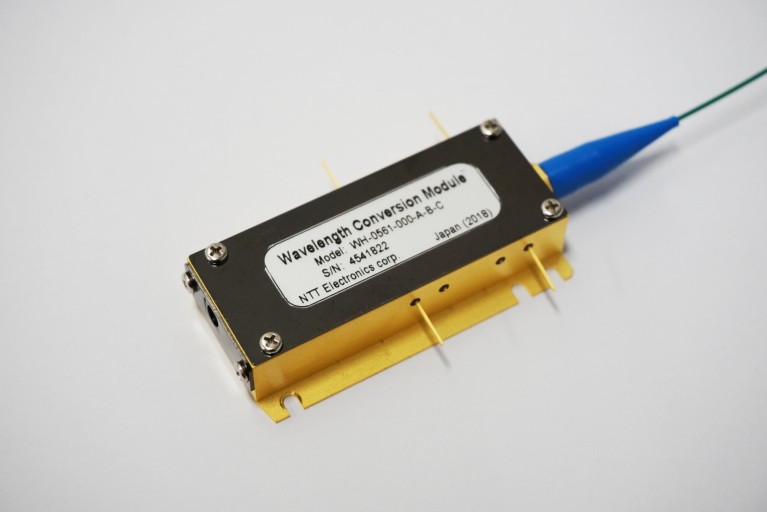
A module that converts the wavelength of light using a non-linear process known as second-harmonic generation.© NTT Electronics Corporation
All-in-one solution
Umeki helped NTT apply their optical technology to quantum computing. In 2016, the team reported progress towards creating an ‘Ising machine’, a type of computer designed to solve complex optimization problems by mimicking a network of magnetic spins. This approach involved creating a network of coupled optical pulses, generated with PPLN waveguides, to represent spins localized inside an optical fibre ring.
NTT’s optical Ising machine was able to solve a 2,000-node optimization problem by searching for strong collective oscillation modes, which indicate minimum-energy configurations. This scalable architecture avoided the challenges of physical spin systems. By 2021, the NTT team had solved up to 100,000-node problems using similar optical technology.
PPLN waveguides can play an important role in the development of a wide range of technologies, including quantum computers, light squeezers and broadband optical-communication networks. “I refer to it as a magic wand — you feel like a wizard because there’s so many applications, from ultralow-noise space communications to wavelength conversion to optical quantum computers,” says Umeki.
This article has been produced with assistance from NTT (Nippon Telegraph and Telephone Corporation).


 Nature Index Japan 2023