
Volume 12 Issue 7, July 2013
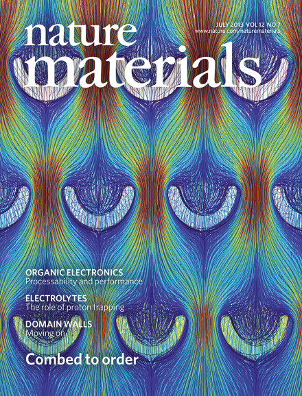
Solution printing of organic semiconductors could in principle be scaled to industrial needs, yet attaining aligned single-crystals directly with this method has been challenging. By using a micropillarpatterned printing blade designed to enhance the control of crystal nucleation and growth, thin films of macroscopic, highly aligned single crystals of organic semiconductors can now be fabricated.
Article p665; News & Views p598
IMAGE: ZHENAN BAO AND YING DIAO
COVER DESIGN: DAVID SHAND
Editorial
-
Advertisement
