Abstract
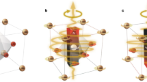
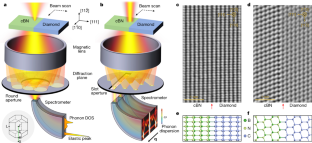
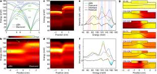
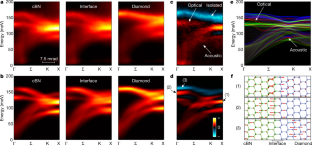
The breakdown of translational symmetry at heterointerfaces leads to the emergence of new phonon modes localized at the interface1. These modes have an essential role in thermal and electrical transport properties in devices, especially in miniature ones wherein the interface may dominate the entire response of the device2. Although related theoretical work began decades ago1,3,4,5, experimental research is totally absent owing to challenges in achieving the combined spatial, momentum and spectral resolutions required to probe localized modes. Here, using the four-dimensional electron energy-loss spectroscopy technique, we directly measure both the local vibrational spectra and the interface phonon dispersion relation for an epitaxial cubic boron nitride/diamond heterointerface. In addition to bulk phonon modes, we observe modes localized at the interface and modes isolated from the interface. These features appear only within approximately one nanometre around the interface. The localized modes observed here are predicted to substantially affect the interface thermal conductance and electron mobility. Our findings provide insights into lattice dynamics at heterointerfaces, and the demonstrated experimental technique should be useful in thermal management, electrical engineering and topological phononics.
This is a preview of subscription content, access via your institution
Access options
Access Nature and 54 other Nature Portfolio journals
Get Nature+, our best-value online-access subscription
$29.99 / 30 days
cancel any time
Subscribe to this journal
Receive 51 print issues and online access
$199.00 per year
only $3.90 per issue
Buy this article
- Purchase on Springer Link
- Instant access to full article PDF
Prices may be subject to local taxes which are calculated during checkout
Data availability
The experimental 3D EELS and 4D EELS datasets are available in the Open Science Framework repository at https://osf.io/8mp4t. The other data that support the findings of this study are available from the corresponding author upon request.
Code availability
A GUI version of the MATLAB code for the EELS data processing can be found on GitHub at https://github.com/ruishiqi/EELS.
References
Masri, P. Surface and interface phonons and related topics. Surf. Sci. Rep. 9, 293–369 (1988).
Giri, A. & Hopkins, P. E. A review of experimental and computational advances in thermal boundary conductance and nanoscale thermal transport across solid interfaces. Adv. Funct. Mater. 30, 1903857 (2020).
Djafari-Rouhani, B., Masri, P. & Dobrzynski, L. Vibrational properties of a bicrystal interface: different-interface phonons and the low-temperature specific heat. Phys. Rev. B 15, 5690–5711 (1977).
Masri, P. Interface phonons: effects of crystal size. J. Phys. C 14, 2265–2278 (1981).
Tamine, M., Boumrar, H. & Rafil, O. Interface and step localized phonon modes between two truncated thin films. Surf. Rev. Lett. 11, 155–165 (2004).
Girvin, S. & Yang, K. Modern Condensed Matter Physics (Cambridge Univ. Press, 2019).
Gordiz, K. & Henry, A. Phonon transport at interfaces: determining the correct modes of vibration. J. Appl. Phys. 119, 015101 (2016).
Luh, D. A., Miller, T., Paggel, J. J. & Chiang, T. C. Large electron–phonon coupling at an interface. Phys. Rev. Lett. 88, 256802 (2002).
Cahill, D. G. et al. Nanoscale thermal transport. J. Appl. Phys. 93, 793–818 (2003).
Chu, C. W. et al. Interface-induced and interface-enhanced superconductivity. J. Supercond. Nov. Magn. 32, 7–15 (2018).
Wang, Q.-Y. et al. Interface-induced high-temperature superconductivity in single unit-cell FeSe films on SrTiO3. Chin. Phys. Lett. 29, 037402 (2012).
Gordiz, K. & Henry, A. Phonon transport at crystalline Si/Ge interfaces: the role of interfacial modes of vibration. Sci. Rep. 6, 23139 (2016).
Burkel, E. Phonon spectroscopy by inelastic X-ray scattering. Rep. Prog. Phys. 63, 171–232 (2000).
Lee, J., Crampton, K. T., Tallarida, N. & Apkarian, V. A. Visualizing vibrational normal modes of a single molecule with atomically confined light. Nature 568, 78–82 (2019).
Chen, X. et al. Modern scattering-type scanning near-field optical microscopy for advanced material research. Adv. Mater. 31, 1804774 (2019).
Szeftel, J. Surface phonon dispersion, using electron energy loss spectroscopy. Surf. Sci. 152/153, 797–810 (1985).
Krivanek, O. L. et al. Vibrational spectroscopy in the electron microscope. Nature 514, 209–212 (2014).
Egerton, R. F. Electron Energy-loss Spectroscopy in the Electron Microscope 3rd edn (Springer, 2011).
Hage, F. S. et al. Nanoscale momentum-resolved vibrational spectroscopy. Sci. Adv. 4, eaar7495 (2018).
Lagos, M. J., Trugler, A., Hohenester, U. & Batson, P. E. Mapping vibrational surface and bulk modes in a single nanocube. Nature 543, 529–532 (2017).
Qi, R. et al. Four-dimensional vibrational spectroscopy for nanoscale mapping of phonon dispersion in BN nanotubes. Nat. Commun. 12, 1179 (2021).
Li, N. et al. Direct observation of highly confined phonon polaritons in suspended monolayer hexagonal boron nitride. Nat. Mater. 20, 43–48 (2021).
Govyadinov, A. A. et al. Probing low-energy hyperbolic polaritons in van der Waals crystals with an electron microscope. Nat. Commun. 8, 95 (2017).
Venkatraman, K., Levin, B. D. A., March, K., Rez, P. & Crozier, P. A. Vibrational spectroscopy at atomic resolution with electron impact scattering. Nat. Phys. 15, 1237–1241 (2019).
Hage, F. S., Radtke, G., Kepaptsoglou, D. M., Lazzeri, M. & Ramasse, Q. M. Single-atom vibrational spectroscopy in the scanning transmission electron microscope. Science 367, 1124–1127 (2020).
Yan, X. et al. Single-defect phonons imaged by electron microscopy. Nature 589, 65–69 (2021).
Senga, R. et al. Position and momentum mapping of vibrations in graphene nanostructures. Nature 573, 247–250 (2019).
Dwyer, C. et al. Electron-beam mapping of vibrational modes with nanometer spatial resolution. Phys. Rev. Lett. 117, 256101 (2016).
Hachtel, J. A. et al. Identification of site-specific isotopic labels by vibrational spectroscopy in the electron microscope. Science 363, 525–528 (2019).
Hage, F. S., Kepaptsoglou, D. M., Ramasse, Q. M. & Allen, L. J. Phonon spectroscopy at atomic resolution. Phys. Rev. Lett. 122, 016103 (2019).
Plotkin-Swing, B. et al. Hybrid pixel direct detector for electron energy loss spectroscopy. Ultramicroscopy 217, 113067 (2020).
Nicholls, R. J. et al. Theory of momentum-resolved phonon spectroscopy in the electron microscope. Phys. Rev. B 99, 094105 (2019).
Fritsch, J., Pavone, P. & Schröder, U. Ab initio calculation of the phonon dispersion in bulk InP and in the InP(110) surface. Phys. Rev. B 52, 11326–11334 (1995).
Benedek, G. et al. Theory of surface phonons at metal surfaces: recent advances. J. Phys. Condens. Matter 22, 084020 (2010).
Little, W. A. The transport of heat between dissimilar solids at low temperatures. Can. J. Phys. 37, 334–349 (1959).
Swartz, E. T. & Pohl, R. O. Thermal boundary resistance. Rev. Mod. Phys. 61, 605–668 (1989).
Mingo, N. & Yang, L. Phonon transport in nanowires coated with an amorphous material: an atomistic Green’s function approach. Phys. Rev. B 68, 245406 (2003).
Gordiz, K. & Henry, A. A formalism for calculating the modal contributions to thermal interface conductance. New J. Phys. 17, 103002 (2015).
Ohtomo, A. & Hwang, H. Y. A high-mobility electron gas at the LaAlO3/SrTiO3 heterointerface. Nature 427, 423–426 (2004).
Chen, C. et al. Misfit accommodation mechanism at the heterointerface between diamond and cubic boron nitride. Nat. Commun. 6, 6327 (2015).
Süsstrunk, R. & Huber, S. D. Observation of phononic helical edge states in a mechanical topological insulator. Science 349, 47–50 (2015).
Li, J. et al. Computation and data driven discovery of topological phononic materials. Nat. Commun. 12, 1204 (2021).
Liu, Y., Xu, Y., Zhang, S.-C. & Duan, W. Model for topological phononics and phonon diode. Phys. Rev. B 96, 064106 (2017).
T. Taniguchi, & S. Yamaoka. Heteroepitaxial growth of cubic boron nitride single crystal on diamond seed under high pressure. Mater. Res. Soc. Symp. Proc. 472, 379–383 (1997).
Chen, K. et al. Ultrahigh thermal conductivity in isotope-enriched cubic boron nitride. Science 367, 555–559 (2020).
Wei, L., Kuo, P. K., Thomas, R. L., Anthony, T. R. & Banholzer, W. F. Thermal conductivity of isotopically modified single crystal diamond. Phys. Rev. Lett. 70, 3764–3767 (1993).
Huang, X. & Guo, Z. High thermal conductance across c-BN/diamond interface. Diam. Relat. Mater. 108, 107979 (2020).
Zhou, J. et al. Observing crystal nucleation in four dimensions using atomic electron tomography. Nature 570, 500–503 (2019).
Dabov, K., Foi, A., Katkovnik, V. & Egiazarian, K. Image denoising by sparse 3-D transform-domain collaborative filtering. IEEE Trans. Image Process. 16, 2080–2095 (2007).
Batson, P. E. & Lagos, M. J. Interpretation of meV resolution phonon EELS data. Microsc. Microanal. 24, 412–413 (2018).
Williams, D. B. & Carter, C. B. Transmission Electron Microscopy: A Textbook for Materials Science Vol. 2 (Springer Science & Business Media, 2008).
Giannozzi, P. et al. Quantum ESPRESSO: a modular and open-source software project for quantum simulations of materials. J. Phys. Condens. Matter 21, 395502 (2009).
Giannozzi, P. et al. Advanced capabilities for materials modelling with Quantum ESPRESSO. J. Phys. Condens. Matter 29, 465901 (2017).
Perdew, J. P. & Zunger, A. Self-interaction correction to density-functional approximations for many-electron systems. Phys. Rev. B 23, 5048–5079 (1981).
Vanderbilt, D. Soft self-consistent pseudopotentials in a generalized eigenvalue formalism. Phys. Rev. B 41, 7892–7895 (1990).
Vila, F. D., Rehr, J. J., Rossner, H. H. & Krappe, H. J. Theoretical X-ray absorption Debye–Waller factors. Phys. Rev. B 76, 014301 (2007).
Waasmaier, D. & Kirfel, A. New analytical scattering-factor functions for free atoms and ions. Acta Crystallogr. A 51, 416–431 (1995).
Plimpton, S. Fast parallel algorithms for short-range molecular dynamics. J. Comput. Phys. 117, 1–19 (1995).
Kınacı, A., Haskins, J. B., Sevik, C. & Çağın, T. Thermal conductivity of BN-C nanostructures. Phys. Rev. B 86, 115410 (2012).
Seyf, H. R., Gordiz, K., DeAngelis, F. & Henry, A. Using Green–Kubo modal analysis (GKMA) and interface conductance modal analysis (ICMA) to study phonon transport with molecular dynamics. J. Appl. Phys. 125, 081101 (2019).
Togo, A., Chaput, L. & Tanaka, I. Distributions of phonon lifetimes in Brillouin zones. Phys. Rev. B 91, 094306 (2015).
Acknowledgements
This work was supported by the National Key R&D Program of China (2019YFA0708200), the National Natural Science Foundation of China (11974023, 52021006, 52125307, 12004010, 11888101), the Key-Area Research and Development Program of Guangdong Province (2018B030327001, 2018B010109009), the Strategic Priority Research Program of Chinese Academy of Sciences (XDB33000000), the ‘2011 Program’ from the Peking-Tsinghua-IOP Collaborative Innovation Center of Quantum Matter, the Youth Innovation Promotion Association of CAS, and the Introduced Innovative R&D Team Project of ‘The Pearl River Talent Recruitment Program’ of Guangdong Province (2019ZT08C321). We acknowledge the Electron Microscopy Laboratory of Peking University for the use of electron microscopes. We acknowledge the High-performance Computing Platform of Peking University for providing computational resources for the DFPT and molecular dynamics calculations. We thank J. Feng, Q. Gu, A. Gabourie, Z. Fan, C. Shi and T. Lovejoy for helpful discussions; and T. Taniguchi at NIMS in Japan for providing the samples.
Author information
Authors and Affiliations
Contributions
R.Q. and R.S. contributed equally to this work (order determined by a random process upon completion of the manuscript). P.G., R.S. and R.Q. conceived the project. C.C. prepared the TEM sample. R.S. designed and performed the EELS measurements. R.Q. wrote the data processing codes and analysed the data. R.S. and R.Q. performed DFPT calculations of phonon dispersion, scattering cross-section and electron–phonon coupling under the direction of E.-G.W. R.Q., Y.L. and R.S. performed molecular dynamics simulations with the guidance from J.C. Y.S., M.W. and Y.L. acquired atomic-resolution iDPC images. N.L., J.D., K.L., F.W. and D.Y helped the data interpretation. R.Q., R.S. and P.G. finalized the manuscript with inputs from F.W. All authors contributed to this work through useful discussion and/or comments to the manuscript. P.G. supervised the project.
Corresponding author
Ethics declarations
Competing interests
The authors declare no competing interests.
Additional information
Peer review information Nature thanks Juan-Carlos Idrobo, Lucas Lindsay and the other, anonymous, reviewer(s) for their contribution to the peer review of this work. Peer reviewer reports are available.
Publisher’s note Springer Nature remains neutral with regard to jurisdictional claims in published maps and institutional affiliations.
Extended data figures and tables
Extended Data Fig. 1 Spatial resolution estimation for 4D EELS.
a, b, Spatial resolution as a function of convergence semi-angle for 60 kV (a) and 30 kV (b) beam energy. Solid line, diffraction limit. Dashed line, theoretical beam size considering both the diffraction limit and the beam source size. Scatters with error bars are experimental fitted resolution as shown in the following panels, where vertical error bars represent the standard deviation of the fitted resolutions from multiple images and horizontal ones are estimated by the roundness of the central diffraction spot. See Methods for detail. c, Momentum resolution as a function of convergence semi-angle. Inset with light-grey shadow schematically shows the diffraction spot size (yellow circles) relative to the BZ size in our 4D EELS measurements. Dashed horizontal lines mark the ratio to the distance between Γ and X. d, HAADF image of gold nanoparticles taken with 35 mrad (nominal value) convergence semi-angle with 60 kV beam energy, serving as a reference image. e–g, Above the yellow line are typical HAADF images taken with 5 mrad, 3 mrad and 2 mrad convergence semi-angles, respectively. Below the yellow line are the reference image convoluted with a Gaussian kernel with FWHM indicated in the title (fitting result), which agrees nicely with the acquired images above the yellow line. h–k, same as d–g, but taken with 30 kV beam energy. Convergence semi-angles are 40 mrad (reference image), 7.5 mrad, 3 mrad, and 2 mrad respectively.
Extended Data Fig. 2 Interface component of the spectra extracted by finding the minimum difference between the measured spectrum and all possible linear combinations of two bulk spectra.
The fitting was performed by minimizing \(\Vert S(\omega )-{a}_{1}{S}_{{\rm{cBN}}}(\omega )-{a}_{2}{S}_{{\rm{diamond}}}(\omega )\Vert \), where S(ω) is the measured spectrum (Fig. 2b), \(S(\omega )\) with subscripts means the bulk spectra, and \({a}_{1},{a}_{2}\) are adjusted coefficients. a, Line profile of the fitting residual. Since the fitting gives the linear combination that is closest to the measured spectrum, the residual represents the interface component that cannot be obtained from bulk modes. Near the interface, three red peaks correspond to three interfacial modes in Fig. 2g. The blue region at 160 meV is due to the isolated mode with reduced vibration at the interface. b, Norm (root sum squared) of residuals as a function of position (left axis), and the fitting coefficients \({a}_{1}\) and \({a}_{2}\) (right axis). The residual is sharply peaked at the interface (FWHM = 1.8 nm), indicating new vibrational features are highly localized at the interface.
Extended Data Fig. 3 3D EELS data acquired in different regions.
a, A low-magnification annular dark field image showing where the datasets were acquired. Boxes with labels ‘3D’ and ‘4D’ correspond to the scanning regions of the 3D EELS and 4D EELS datasets discussed in the main text. b–e, Four EELS line profiles acquired under the same experimental conditions except different pixel sizes and different scanning regions (marked in a). b, c and d, e were acquired in two experiments that were two weeks apart. All datasets give consistent results as the one shown in Fig. 2.
Extended Data Fig. 4 Off-axis EELS measurements.
a, A schematic of the diffraction plane and EELS aperture placement. The colormap illustrates the diffraction plane viewed from \([11\bar{2}]\) zone axis, with 60 kV beam energy and 35 mrad convergence semi-angle. The diffraction spot size (35 mrad) is larger than the distance between adjacent spots, so they partially overlap. The green circle marks the position of the aperture, which is displaced away from the central spot. b, The EELS line profile acquired with off-axis geometry. Main spectral features are consistent with those acquired with on-axis geometry (Fig. 2b, Extended Data Fig. 3). c, Corresponding simulation result. d, EELS maps at selected energies. One of the interfacial modes has a better contrast than the on-axis result. e–h, same as a–d, but the beam is travelling along \([1\bar{1}0]\) direction.
Extended Data Fig. 5 Phonon dispersion diagrams measured with 3 mrad convergence semi-angle.
a, A schematic of the bulk BZ (truncated octahedron) and the interface two-dimensional BZ (yellow hexagon). Upper-case and lower-case letters mark the high-symmetry points of the bulk BZ and interface BZ, respectively. b, Measured dispersion diagrams along the Γ–Σ–K–X line with 3 mrad convergence semi-angle. Dashed curves are calculated bulk phonon dispersion. Although smaller convergence semi-angles give better momentum resolution and hence nicer dispersion diagrams, insufficient spatial resolution makes it hard to extract localized features at the interface.
Extended Data Fig. 6 EELS line profiles at five momentum transfers.
a, A schematic of the diffraction plane and EELS aperture placement. The colormap illustrates the diffraction plane viewed from \([11\bar{2}]\) zone axis, with 30 kV beam energy and 7.5 mrad convergence semi-angle. The diffraction spot size is drawn to scale, indicating our momentum resolution. The green rectangle marks the position of the slot aperture. b–f, Line profiles with momentum transfers from Γ (b) through the Σ line (c, d) to K (e) and finally X (f). The intensity decrease of the highest-frequency optical phonon is observable in most panels (green arrows), which corresponds to the negative-intensity line at 150-160 meV in Fig. 3c, d. The interfacial mode is directly observable in some panels (white arrows).
Extended Data Fig. 7 Projected bulk phonon bands.
a, b, Bulk phonon band of cBN and diamond projected onto (111) surface.
Extended Data Fig. 8 Modal contribution to ITC.
a, ITC decomposed into the mode-mode correlation integrals (Methods), with modes binned by their frequency. 8640 eigen modes are divided into 100 frequency bins. Main panel, pseudo-colour map of ITC component Gnn’ from heat flux correlation between nth and n’th frequency bin. Colour scale is in units of GW m−2 K−1. Qualitatively it gives a measure of how strong two modes interact with each other. Right panel shows modal thermal conductance Gn in the nth frequency bin, i.e., projecting the Gnn’ map along one dimension. Top panel is a scatter plot showing the frequency versus interface vibration amplitude for each eigen mode. Interfacial modes show strong correlation with almost all other modes (red arrows), while isolated modes have almost no correlation with any other modes (green arrow) b, ITC decomposed into the mode-mode correlation integrals, with modes sorted by their interfacial amplitudes. The same set of eigen modes are sorted by their amplitudes at the interface, aiming to visualize the relation between interfacial amplitudes and modal thermal conductance. For clarity, eigenvectors are normalized such that the squared norm of each eigenvector is the number of atoms (this is just an overall scaling of all eigenvectors), so an interfacial amplitude greater than one means an enhanced vibration at the interface and a value smaller than one means a reduced vibration at the interface. Main panel shows the per-mode (i.e., divided by the number of modes in each bin) contribution to ITC from the modal heat flux correlation between nth and n’th amplitude bin. Colour scale is in units of MW m−2 K−1. Modes with enhanced amplitudes at the interface show strong correlation with all other modes, while modes with reduced amplitudes at the interface show little correlation with other modes. Top panel gives the scatter plot of frequency versus interfacial amplitude again.
Extended Data Fig. 9 Electron-phonon coupling at the interface calculated by DFPT.
a, Phonon linewidth due to electron-phonon coupling mapped on the phonon dispersion. Compared with bulk modes, the interfacial optical modes couple strongly with electrons (note that the colour map is in log scale) because both the interfacial phonon modes and the two-dimensional electron gas are highly confined at the interface. b, Electronic band structure. Three RGB channels represent electron wavefunctions projected onto atomic orbitals in the interface region (red), in cBN (green) and in diamond (blue). Dashed horizontal line is the Fermi level, which crosses a band localized near the interface, meaning the system becomes metallic due to carriers at the interface.
Supplementary information
Supplementary Video 1
Four-dimensional EELS dataset across the interface. The top panel shows the energy-filtered EELS map between 120 meV and 140 meV at the Γ point, which includes the TO phonon of cBN but no phonon modes of diamond. The red dot or red vertical line indicates the beam position. The bottom panel compares the experimental and calculated dispersion diagram as the beam scans on the sample.
Rights and permissions
About this article
Cite this article
Qi, R., Shi, R., Li, Y. et al. Measuring phonon dispersion at an interface. Nature 599, 399–403 (2021). https://doi.org/10.1038/s41586-021-03971-9
Received:
Accepted:
Published:
Issue Date:
DOI: https://doi.org/10.1038/s41586-021-03971-9
This article is cited by
-
Single-atom vibrational spectroscopy with chemical-bonding sensitivity
Nature Materials (2023)
-
Phonon transition across an isotopic interface
Nature Communications (2023)
-
Interfacial interaction and intense interfacial ultraviolet light emission at an incoherent interface
Nature Communications (2023)
-
A review of thermal properties of CVD diamond films
Journal of Materials Science (2023)
-
Isotopes tracked on a sub-nanometre scale using electron spectroscopy
Nature (2022)
Comments
By submitting a comment you agree to abide by our Terms and Community Guidelines. If you find something abusive or that does not comply with our terms or guidelines please flag it as inappropriate.


