Abstract
The most promising quantum algorithms require quantum processors that host millions of quantum bits when targeting practical applications1. A key challenge towards large-scale quantum computation is the interconnect complexity. In current solid-state qubit implementations, an important interconnect bottleneck appears between the quantum chip in a dilution refrigerator and the room-temperature electronics. Advanced lithography supports the fabrication of both control electronics and qubits in silicon using technology compatible with complementary metal oxide semiconductors (CMOS)2. When the electronics are designed to operate at cryogenic temperatures, they can ultimately be integrated with the qubits on the same die or package, overcoming the ‘wiring bottleneck’3,4,5,6. Here we report a cryogenic CMOS control chip operating at 3 kelvin, which outputs tailored microwave bursts to drive silicon quantum bits cooled to 20 millikelvin. We first benchmark the control chip and find an electrical performance consistent with qubit operations of 99.99 per cent fidelity, assuming ideal qubits. Next, we use it to coherently control actual qubits encoded in the spin of single electrons confined in silicon quantum dots7,8,9 and find that the cryogenic control chip achieves the same fidelity as commercial instruments at room temperature. Furthermore, we demonstrate the capabilities of the control chip by programming a number of benchmarking protocols, as well as the Deutsch–Josza algorithm10, on a two-qubit quantum processor. These results open up the way towards a fully integrated, scalable silicon-based quantum computer.
This is a preview of subscription content, access via your institution
Access options
Access Nature and 54 other Nature Portfolio journals
Get Nature+, our best-value online-access subscription
$29.99 / 30 days
cancel any time
Subscribe to this journal
Receive 51 print issues and online access
$199.00 per year
only $3.90 per issue
Buy this article
- Purchase on Springer Link
- Instant access to full article PDF
Prices may be subject to local taxes which are calculated during checkout

Data availability
Data supporting this work are available at https://doi.org/10.5281/zenodo.4061970.
Code availability
The codes used for data acquisition and processing are from the open-source Python packages QCoDeS (available at https://github.com/QCoDeS/Qcodes), QTT (available at https://github.com/QuTech-Delft/qtt) and PycQED (available at https://github.com/DiCarloLab-Delft/PycQED_py3).
References
Van Meter, R. & Horsman, C. A blueprint for building a quantum computer. Commun. ACM 56, 84–93 (2013).
Pillarisetty, R. et al. Qubit device integration using advanced semiconductor manufacturing process technology. In 2018 IEEE International Electron Devices Meeting 6.3.1–6.3.4 (IEEE, 2018).
Vandersypen, L. M. K. et al. Interfacing spin qubits in quantum dots and donors—hot, dense, and coherent. npj Quantum Inf. 3, 34 (2017).
Patra, B. et al. Cryo-CMOS circuits and systems for quantum computing applications. IEEE J. Solid-State Circuits 53, 309–321 (2018).
Pauka, S. J. et al. A cryogenic CMOS chip for generating control signals for multiple qubits. Nat. Electronics 4, 64–70 (2021).
Geck, L., Kruth, A., Bluhm, H., van Waasen, S. & Heinen, S. Control electronics for semiconductor spin qubits. Quantum Sci. Technol. 5, 015004 (2019).
Watson, T. F. et al. A programmable two-qubit quantum processor in silicon. Nature 555, 633–637 (2018).
Zajac, D. M. et al. Resonantly driven CNOT gate for electron spins. Science 359, 439–442 (2018).
Huang, W. et al. Fidelity benchmarks for two-qubit gates in silicon. Nature 569, 532–536 (2019).
Deutsch, D. & Jozsa, R. Rapid solution of problems by quantum computation. Proc. R. Soc. Lond. A 439, 553–558 (1992).
Arute, F. et al. Quantum supremacy using a programmable superconducting processor. Nature 574, 505–510 (2019).
Bardin, J. C. et al. Design and characterization of a 28-nm bulk-CMOS cryogenic quantum controller dissipating less than 2 mW at 3 K. IEEE J. Solid-State Circuits 54, 3043–3060 (2019).
Patra, B. et al. A scalable cryo-CMOS 2-to-20GHz digitally intensive controller for 4 × 32 frequency multiplexed spin qubits/transmons in 22nm FinFET technology for quantum computers. In 2020 IEEE International Solid-State Circuits Conference 304–306 (IEEE, 2020).
Le Guevel, L. et al. A 110mK 295μW 28nm FDSOI CMOS quantum integrated circuit with a 2.8 GHz excitation and nA current sensing of an on-chip double quantum dot. In 2020 IEEE International Solid-State Circuits Conference 306–308 (IEEE, 2020).
Bonen, S. et al. Cryogenic characterization of 22-nm FDSOI CMOS technology for quantum computing ICs. IEEE Electron. Device Lett. 40, 127–130 (2018).
Esmailiyan, A. et al. A fully integrated DAC for CMOS position-based charge qubits with single-electron detector loopback testing. IEEE Solid-State Circuits Lett. 3, 354–357 (2020).
Ekanayake, S. R. et al. Characterization of SOS-CMOS FETs at low temperatures for the design of integrated circuits for quantum bit control and readout. IEEE Trans. Electron Dev. 57, 539–547 (2010).
Mukhanov, O. et al. Scalable quantum computing infrastructure based on superconducting electronics. In 2019 IEEE International Electron Devices Meeting 31.2.1–31.2.4 (IEEE, 2019).
Xu, Y. et al. On-chip integration of Si/SiGe-based quantum dots and switched-capacitor circuits. Appl. Phys. Lett. 117, 144002 (2020).
Batey, G., Matthews, A. J. & Patton, M. A new ultralow- temperature cryogen-free experimental platform. J. Phys. Conf. Ser. 568, 032014 (2014).
Green, M. A. The cost of coolers for cooling superconducting devices at temperatures at 4.2 K, 20 K, 40 K and 77 K. In IOP Conference Series: Materials Science and Engineering Vol. 101, 012001 (IOP, 2015).
Petit, L. et al. Universal quantum logic in hot silicon qubits. Nature 580, 355–359 (2020).
Yang, C. H. et al. Operation of a silicon quantum processor unit cell above one kelvin. Nature 580, 350–354 (2020).
Urdampilleta, M. et al. Gate-based high fidelity spin readout in a CMOS device. Nat. Nanotechnol. 14, 737–741 (2019).
van Dijk, J. P. G. et al. Designing a DDS-based SoC for high-fidelity multi-qubit control. IEEE Trans. Circuits Syst. I 67, 5380–5393 (2020).
Beckers, A., Jazaeri, F. & Enz, C. Characterization and modeling of 28-nm bulk CMOS technology down to 4.2 K. IEEE J. Electr. Dev. Soc. 6, 1007–1018 (2018).
Hart, P. A. T., Babaie, M., Charbon, E., Vladimirescu, A. & Sebastiano, F. Subthreshold mismatch in nanometer CMOS at cryogenic temperatures. IEEE J. Electr. Dev. Soc. 8, 797–806 (2020).
Patra, B. et al. Characterization and analysis of on-chip microwave passive components at cryogenic temperatures. IEEE J. Electr. Dev. Soc. 8, 448–456 (2020).
Pioro-Ladrière, M. et al. Electrically driven single-electron spin resonance in a slanting Zeeman field. Nat. Phys. 4, 776–779 (2008).
Vandersypen, L. M. K. & Chuang, I. L. NMR techniques for quantum control and computation. Rev. Mod. Phys. 76, 1037–1069 (2005).
Petta, J. R. et al. Coherent manipulation of coupled electron spins in semiconductor quantum dots. Science 309, 2180–2184 (2005).
Meunier, T., Calado, V. E. & Vandersypen, L. M. K. Efficient controlled-phase gate for single-spin qubits in quantum dots. Phys. Rev. B 83, 121403 (2011).
Xue, X. et al. Repetitive quantum nondemolition measurement and soft decoding of a silicon spin qubit. Phys. Rev. X 10, 021006 (2020).
Saul, P. H. & Mudd, M. S. J. A direct digital synthesizer with 100-MHz output capability. IEEE J. Solid-State Circuits 23, 819–821 (1988).
Reed, M. Entanglement and Quantum Error Correction with Superconducting Qubits. PhD Thesis, Yale Univ. (2013).
Altepeter, J. B., Jeffrey, E. R. & Kwiat, P. G. Photonic state tomography. Adv. At. Mol. Opt. Phys. 52, 105–159 (2005).
Knill, E. et al. Randomized benchmarking of quantum gates. Phys. Rev. A 77, 012307 (2008).
Magesan, E., Gambetta, J. M. & Emerson, J. Characterizing quantum gates via randomized benchmarking. Phys. Rev. A 85, 042311 (2012).
Fowler, A. G., Mariantoni, M., Martinis, J. M. & Cleland, A. N. Surface codes: towards practical large-scale quantum computation. Phys. Rev. A 86, 032324 (2012).
Svore, K. M., Aho, A. V., Cross, A. W., Chuang, I. & Markov, I. L. A layered software architecture for quantum computing design tools. Computer 39, 74–83 (2006).
Preskill, J. Quantum computing in the NISQ era and beyond. Quantum 2, 79 (2018).
Boter, J. M. et al. A sparse spin qubit array with integrated control electronics. In 2019 IEEE International Electron Devices Meeting 31.4.1–31.4.4 (IEEE, 2019).
Sabbagh, D. et al. Quantum transport properties of industrial 28Si/28SiO2. Phys. Rev. Appl. 12, 014013 (2019).
Lawrie, W. I. L. et al. Quantum dot arrays in silicon and germanium. Appl. Phys. Lett. 116, 080501 (2020).
Zinner, E. Depth profiling by secondary ion mass spectrometry. Scanning 3, 57–78 (1980).
Srinivasa, V. et al. Simultaneous spin-charge relaxation in double quantum dots. Phys. Rev. Lett. 110, 196803 (2013).
Acknowledgements
This research was funded by Intel Corporation. We acknowledge discussions with the members in the Spin Qubit team, the Cryo-CMOS team and Intel Corporation, and technical assistance by O. Benningshof, M. Sarsby, R. Schouten and R. Vermeulen.
Author information
Authors and Affiliations
Contributions
X.X., B.P. and J.P.G.v.D. performed the experiment. N.S. fabricated the quantum device. A.S., B.P.W. and G.S. designed, grew and characterized the Si/SiGe heterostructure. A.C. contributed to the preparation of the experiment. X.X. and B.P. analysed the data presented in the main manuscript. F. Sebastiano, M.B., S.P., E.C. and L.M.K.V. conceived and supervised the project. X.X., B.P. and L.M.K.V. wrote the manuscript with input from all authors.
Corresponding authors
Ethics declarations
Competing interests
The authors declare no competing interests.
Additional information
Peer review information Nature thanks Fernando Gonzalez-Zalba, Stefan van Waasen and the other, anonymous, reviewer(s) for their contribution to the peer review of this work. Peer reviewer reports are available.
Publisher’s note Springer Nature remains neutral with regard to jurisdictional claims in published maps and institutional affiliations.
Extended data figures and tables
Extended Data Fig. 1 Experiment setup.
The quantum dot device is wire-bonded onto a PCB placed on a cold finger attached to the mixing chamber plate (~20 mK) of a dilution refrigerator (Bluefors XLD). Voltage pulses onto gates RP and LP are generated by the AWG at RT, and go through a low-pass filter (Minicircuits) and attenuators before reaching the device. These pulses are used to control the electrochemical potentials of the quantum dots and load/unload electrons from/to the electron reservoir (see Extended Data Fig. 6). A programmable mechanical switch at 3 K is used to connect gate MW either to a vector signal generator (VSG) at RT or to the cryo-controller at 3 K (represented as two boxes next to the switch) through a 12–14 GHz band-pass filter to filter out wide-band noise. The mechanical switch can also be configured to send the output signals from the cryo-controller to the oscilloscope and the spectrum analyser at RT for electrical characterization in the time and frequency domains. The cryo-controller is programmed via an FPGA to generate the microwave bursts using an external LO signal and a clock (CLK) signal from a microwave signal generator (MSG) at RT. The SET next to the quantum dots is voltage-biased, and the current signal (ISET) through it is converted to a voltage signal through a transimpedance amplifier and digitized by a digitizer card after an analogue low-pass filter employed to remove out-of-band (>10 kHz) noise. ISET is sensitive to the charge occupation of the quantum dots, allowing binary single-shot readout of the qubit states via spin-to-charge conversion (Extended Data Fig. 6).
Extended Data Fig. 2 Dilution refrigerator setup.
a, Location of the cryo-controller and the quantum device inside the dilution refrigerator (left). Top and bottom views of the 3-K plate, showing the mounted chip enclosure and the fixed holder for the enclosure, respectively (right). b, Top view of the gold-plated annealed copper enclosure (without the lid), which is used to mount and thermalize the cryo-controller. c, Ball-grid array (BGA 324) package hosting the cryo-controller chip with on-package decoupling capacitors (shown as a white box in b). d, The Wilkinson power divider (WPD) splits the input LO power into two equal paths with half power in each, implemented on a PCB. Discrete I/Q hybrids that create the in-phase and quadrature-phase components of the input LO are wire-bonded on the PCB for LO distribution between the different transmitters inside the cryo-controller (shown as a red box in b).
Extended Data Fig. 3 Detailed cryo-controller schematic.
a, Detailed representation of the digital circuitry. b. Detailed system-level schematic of the analogue circuity inside the controller.
Extended Data Fig. 4 Power consumption and self-heating of the cryo-controller.
a, Power-consumption pie chart showing the contribution of the digital and analogue circuits in the cryo-controller. A breakdown of the power consumption of individual circuit blocks is shown for the analogue circuits. The digital circuits use a 0.7-V supply and the analogue circuits use a 1-V supply. b, Chip micrograph showing the on-chip bumps used as inputs/outputs. The locations of on-chip temperature-sensing diodes and the analogue and digital circuitry (in TX0) are highlighted. c, On-chip and 3-K plate temperature, measured using different sensors, versus the power consumption of TX0, as reported in ref. 13. The power consumption is varied by changing the clock frequency of the chip. The nominal operating point for the work presented here and the corresponding temperatures are highlighted with a dashed vertical line. All the other transmitters (TX1, TX2, TX3) are switched off in this measurement.
Extended Data Fig. 5 Detailed electrical characterization of the cryo-controller.
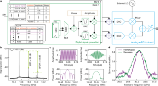
a, Schematic of the output driver (complete version in Extended Data Fig. 3) showing the two different RF outputs, which use the same external LO to generate two different frequencies—that is, a 1-GHz band around the LO frequency (fLO) or a 1-GHz band around 3 × fLO—by selecting the ‘RF-Low’ or ‘RF-High’ path, respectively. RF-High uses the third harmonic output of the mixer to generate the tone around 3 × fLO. b, Peak output power versus frequency generated using the RF-Low and RF-High path, respectively, as reported in ref. 13. The output power can be lowered by up to 40 dB below the peak power in the entire frequency range; for example, at 6 GHz the amplitude range is from −56 dBm to −16 dBm. c, Two-tone output spectrum of the cryo-controller used in the simultaneous Rabi oscillation experiment. d, SNR and SFDR of the cryo-controller at various NCO frequencies around 13.54 GHz.
Extended Data Fig. 6 Pulsing scheme used in qubit experiments.
a, Charge-stability diagram of the DQD system, showing the differential current signal (dISET/dVRP) and charge occupation (M, N) (where M denotes the number of electrons in the dot below LP and N represents the number of electrons in the dot below RP) as a function of the voltages applied to gates LP (VLP) and RP (VRP). The three main stages of a typical pulse sequence are marked by the numbered circles. The gate voltages of stage 3 vary between different experiments: in the experiments with exchange coupling turned on, owing to the cross-capacitance between the barrier (gate T) and the plungers (gates RP and LP), the LP and RP voltages differ from those in the experiments without exchange coupling by ~15 mV. b, Schematic representations of the DQD system during the experiment cycle. Q1 is first initialized to its ground state (spin down) via fast relaxation by pulsing to the charge transition line between (1, 0) and (0, 1) (stage 1), which is a spin-relaxation hotspot46. Then, Q2 is initialized by pulsing it to the transition line between (1, 0) and (1, 1) (stage 2), where the Fermi energy of the electron reservoir is placed in between the two spin states of Q2. This allows a spin-down electron to tunnel into the dot but forbids spin-up electrons from tunnelling in—a mechanism called spin-selective tunnelling. During the qubit operations, the system is pulsed to the middle of the (1, 1) region (stage 3), so both electrons are well confined inside the DQD. The barrier (gate T) voltage is used to turn off the exchange coupling between the two spins in the operation of uncoupled qubits (all measurements in Fig. 3) and to turn on the coupling for two-qubit logic operations (all measurements in Fig. 4). After the operations, the Q2 state is read out via spin-selective tunnelling and reinitialized into the spin-down state (stage 2). The state of Q1 is read out by mapping its state onto Q2 via a two-qubit CROT gate (stage 3), followed by readout of Q2 again (stage 2).
Extended Data Fig. 7 Magnetic field gradient.
a, Wafer stack schematic with corresponding layer thicknesses. b, Depth concentration SIMS profile of 28Si (red), 29Si (blue), 30Si (purple), Ge (black), oxygen (green) and carbon (blue). The residual 29Si concentration in the quantum well is 0.08%, considerably reducing qubit decoherence due to hyperfine interaction. Both carbon and oxygen concentrations are below their respective detection limits of 3 × 1016 cm−3 and 1 × 1017 cm−3. c, Schematic showing the first and second Al gate layers in green and purple, respectively. A cobalt micro-magnet is located on top of the metallic gates (pink-shaded area). d, The micromagnet is magnetized by sweeping the external magnetic field (in the \(\hat{z}\) direction) from 0 to 3 T and back to 380 mT. The magnetized micro-magnet provides an additional magnetic field (brown dashed lines) that has a longitudinal (\(\hat{z}\)) component with a field gradient along the double quantum dots. This longitudinal magnetic field gradient (light blue arrows) makes the Zeeman splittings (resonance frequencies) of the two qubits different by ~110 MHz. Additionally, the micro-magnet also induces a transverse (\(\hat{x}\)) magnetic field gradient (green arrows). When a microwave pulse is sent to the device through gate MW, the wave functions of the electrons are oscillating in the \(\hat{z}\) direction. If the microwave frequency is in resonance with the qubit frequency, the electron is subject to an oscillating magnetic field along the \(\hat{x}\) direction, which induces electric-dipole spin resonance29.
Extended Data Fig. 8 Electron temperature measured at different configurations.
a, b, SET current signal (ISET) as a function of RP voltage (VRP) measured at the charge transition between (1, 0) and (1, 1) when the quantum device is connected to the VSG (a) and to the cryo-controller (b) (at zero magnetic field). The electron temperatures are extracted by fitting the curves with the Fermi–Dirac distribution, with a lever arm of 0.172 eV V−1. The measurements indicate that the output noise of the cryo-controller does not affect the electron temperature more than the noise from the RT setup reduced by 6 dB at the 3-K plate.
Extended Data Fig. 9 Rabi oscillations of qubits individually driven by the cryo-controller.
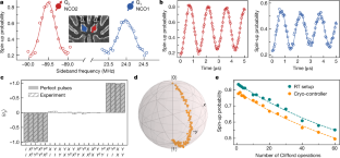
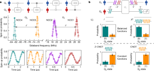
The output frequency of two NCOs are set to the frequencies of Q1 and Q2, respectively, but only one NCO is active each time. Using the same method as described in the main text, the Rabi oscillations of Q1 (a) and Q2 (b) are measured individually. Compared to the simultaneous Rabi oscillations shown in Fig. 3b, the decay is much slower in the individual driving experiments.
Supplementary information
Rights and permissions
About this article
Cite this article
Xue, X., Patra, B., van Dijk, J.P.G. et al. CMOS-based cryogenic control of silicon quantum circuits. Nature 593, 205–210 (2021). https://doi.org/10.1038/s41586-021-03469-4
Received:
Accepted:
Published:
Issue Date:
DOI: https://doi.org/10.1038/s41586-021-03469-4
This article is cited by
-
Non-symmetric Pauli spin blockade in a silicon double quantum dot
npj Quantum Information (2024)
-
Hamiltonian phase error in resonantly driven CNOT gate above the fault-tolerant threshold
npj Quantum Information (2024)
-
Shared control of a 16 semiconductor quantum dot crossbar array
Nature Nanotechnology (2024)
-
Impact of Deep Cryogenic Temperatures on High-k Stacked Dual Gate Junctionless MOSFET Performance: Analog and RF analysis
Silicon (2024)
-
Electrical control of transient formation of electron-hole coexisting system at silicon metal-oxide-semiconductor interfaces
Communications Physics (2023)
Comments
By submitting a comment you agree to abide by our Terms and Community Guidelines. If you find something abusive or that does not comply with our terms or guidelines please flag it as inappropriate.


